

Page 1
Ordering number : EN4863
O3194TH (OT) B8-1281 No. 4863-1/7
Overview
The LC7536R is an electronic volume control IC that
implements volume and balance functions with a
minimum number of external components.
Features
• The LC7536R is controlled by a 3-wire (DI, CL and CE)
serial data control scheme that can be shared with other
ICs. Up to two LC7536Rs can be used on the same bus
by using the S (select) pin.
• Eighty positions in 1 dB steps plus mute (–∞), maximum
attenuation is over 80 dB
• Input impedance (5 dB inputs): 47 kΩ (typical)
• High breakdown voltage: ±16 V
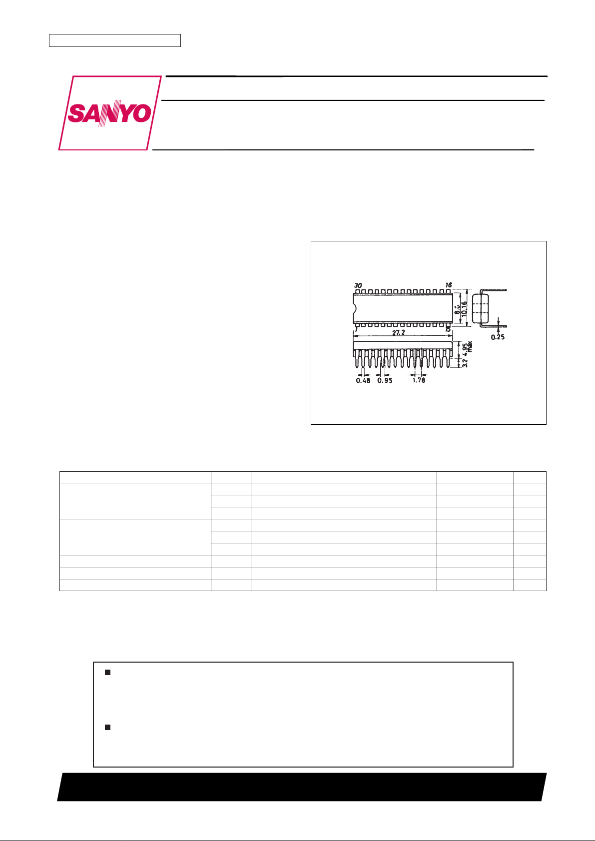
Package Dimensions
unit: mm
3047A-DIP30S
SANYO: DIP30S
[LC7536R]
LC7536R
SANYO Electric Co.,Ltd. Semiconductor Bussiness Headquarters
TOKYO OFFICE Tokyo Bldg., 1-10, 1 Chome, Ueno, Taito-ku, TOKYO, 110-8534 JAPAN
High Breakdown Voltage Serial Control Electronic
Volume Control
CMOS LSI
Any and all SANYO products described or contained herein do not have specifications that can handle
applications that require extremely high levels of reliability, such as life-support systems, aircraft’s
control systems, or other applications whose failure can be reasonably expected to result in serious
physical and/or material damage. Consult with your SANYO representative nearest you before using
any SANYO products described or contained herein in such applications.
SANYO assumes no responsibility for equipment failures that result from using products at values that
exceed, even momentarily, rated values (such as maximum ratings, operating condition ranges, or other
parameters) listed in products specifications of any and all SANYO products described or contained
herein.
Specifications
Absolute Maximum Ratings at Ta = 25°C, VSS= 0 V
Parameter Symbol Conditions Ratings Unit
V
DD
max VEE≤ VSS< VCC< V
DD
VSSto VSS+ 18 V
Maximum supply voltage V
EE
max VEE≤ VSS< VCC< V
DD
VSS– 18 to V
SS
V
V
CC
max VEE≤ VSS< VCC< V
DD
VSSto VSS+ 7 V
V
I
1 CL, DI, CE 0 to VDD+ 0.3 V
Input voltage V
I
2 IN1, IN2 VEE– 0.3 to VDD+ 0.3 V
V
I
3S VCC– 0.3 to VDD+ 0.3 V
Allowable power dissipation Pd max Ta ≤ 75°C 250 mW
Operating temperature Topr –30 to +75 °C
Storage temperature Tstg –40 to +125 °C
Page 2
Allowable Operating Ranges at Ta = 25°C, VSS= 0 V
Electrical Characteristics at Ta = 25°C, VSS= 0 V
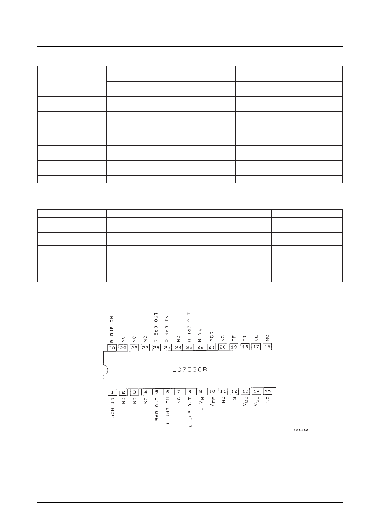
Pin Assignment
No. 4863-2/7
LC7536R
Parameter Symbol Conditions min typ max Unit
V
DD
VCC+ 4.5 16 V
Supply voltage V
EE
–16 0 V
V
CC
4.5 5 5.5 V
Input high level voltage V
IH
1 CL, DI, CE 0.8 V
CC
V
CC
V
Input low level voltage V
IL
1 CL, DI, CE V
SS
0.2 V
CC
V
Input high level voltage V
IH
2 S
0.8
× (VDD–
V
DD
V
V
CC
) + V
CC
Input low level voltage VIL2 S V
CC
0.2 × (VDD–
V
V
CC
) + V
CC
Input pulse width tøw CL 1 µs
Setup time t
set up
CL, DI, CE 1 µs
Hold time t
hold
CL, DI, CE 1 µs
Operating frequency f
opg
CL 500 kHz
Input signal amplitude V
IN
IN1, IN2 V
EE
V
DD
V
Input leakage current I
IN
CL, DI, CE, S –10 +10 µA
Parameter Symbol Conditions min typ max Unit
Current drain
I
DD
1 mA
I
CC
1 mA
Output off leakage current I
OFF
IN1, IN2, VM1, VM2, CT1, CT2, OUT1, OUT2,
–10 +10 µA
analog switch off
Total harmonic distortion
THD1 V
IN
= 1 Vrms, f = 1 kHz, VDD– VEE= 32 V, VR= max 0.004 %
THD2 V
IN
= 0.1 Vrms, f = 1 kHz, VDD– VEE= 32 V, VR= max 0.02 %
Inter-channel crosstalk C
T
OUT1 and OUT2, with a 20 kHz 1 Vrms input to
–75 –60 dB
one channel
Output at maximum attenuation V
O
f = 20 kHz, VIN= 1 Vrms –98 dB
Top view
Page 3

No. 4863-3/7
LC7536R
Equivalent Circuit Block Diagram
Internal Resistor Equivalent Circuit Diagram
unit (resistance: KΩ)
Page 4

Pin Functions
No. 4863-4/7
LC7536R
Pin No. Symbol Function Note
1
30
3
4
28
27
5
26
6
25
8
23
9
22
12
17
18
19
10
13
14
21
2, 7, 11,
15, 16,
20, 24,
29
L 5dBIN
R 5dBIN
NC
NC
NC
NC
L 5dBOUT
R 5dBOUT
L 1dBIN
R 1dBIN
L 1dBOUT
R 1dBOUT
L V
M
R V
M
S
CL
DI
CE
V
EE
V
DD
V
SS
V
CC
NC
Inputs to the 5 dB step attenuator. Must be driven by low impedance outputs.
No connection
Outputs from the 5 dB step attenuator. Outputs should be received by a load of
about 1 MΩ.
Inputs to the 1 dB step attenuator. Must be driven by low impedance outputs.
Outputs from the 1 dB step attenuator. Outputs should be received by a load in the
range 47 kΩ to 1 MΩ.
Volume control common connections. The impedance of the pattern connected to
these pins should be lowered as far as possible. Since LV
M
, RVMand VSSare not
connected internally, they should be connected externally according to their respective
specifications. In particular, when a single-sided power supply is used, the capacitor
connected between V
M
and VSSappears as the residual resistance when the volume
is attenuated. Thus care is required when selecting the value for this capacitor.
Selection pin for the address code in the data format. When this pin is connected to
V
DD
, the LC7536R will accept data when the address code is 9 and when connected
to V
CC
, the LC7536R will accept data when the address code is 8.
Inputs for controlling the LC7536R from serial data. Signals should have an amplitude
of 0 to 5 V.
Power supply connections. Do not bring up the V
CC
voltage before the VDDvoltage
when powering up the LC7536R.
No connection
Page 5

Data Format
No. 4863-5/7
LC7536R
Page 6

Sample Application Circuit
No. 4863-6/7
LC7536R
Page 7

PS No. 4863-7/7
LC7536R
This catalog provides information as of August, 1998. Specifications and information herein are subject to
change without notice.
Specifications of any and all SANYO products described or contained herein stipulate the performance,
characteristics, and functions of the described products in the independent state, and are not guarantees
of the performance, characteristics, and functions of the described products as mounted in the customer’s
products or equipment. To verify symptoms and states that cannot be evaluated in an independent device,
the customer should always evaluate and test devices mounted in the customer’s products or equipment.
SANYO Electric Co., Ltd. strives to supply high-quality high-reliability products. However, any and all
semiconductor products fail with some probability. It is possible that these probabilistic failures could
give rise to accidents or events that could endanger human lives, that could give rise to smoke or fire,
or that could cause damage to other property. When designing equipment, adopt safety measures so
that these kinds of accidents or events cannot occur. Such measures include but are not limited to protective
circuits and error prevention circuits for safe design, redundant design, and structural design.
In the event that any and all SANYO products described or contained herein fall under strategic
products (including services) controlled under the Foreign Exchange and Foreign Trade Control Law of
Japan, such products must not be exported without obtaining export license from the Ministry of
International Trade and Industry in accordance with the above law.
No part of this publication may be reproduced or transmitted in any form or by any means, electronic or
mechanical, including photocopying and recording, or any information storage or retrieval system,
or otherwise, without the prior written permission of SANYO Electric Co., Ltd.
Any and all information described or contained herein are subject to change without notice due to
product/technology improvement, etc. When designing equipment, refer to the “Delivery Specification”
for the SANYO product that you intend to use.
Information (including circuit diagrams and circuit parameters) herein is for example only; it is not
guaranteed for volume production. SANYO believes information herein is accurate and reliable, but
no guarantees are made or implied regarding its use or any infringements of intellectual property rights
or other rights of third parties.
 Loading...