

Page 1
Any and all SANYO products described or contained herein do not have specifications that can handle
applications that require extremely high levels of reliability, such as life-support systems, aircraft’s
control systems, or other applications whose failure can be reasonably expected to result in serious
physical and/or material damage. Consult with your SANYO representative nearest you before using
any SANYO products described or contained herein in such applications.
SANYO assumes no responsibility for equipment failures that result from using products at values that
exceed, even momentarily, rated values (such as maximum ratings, operating condition ranges,or other
parameters) listed in products specifications of any and all SANYO products described or contained
herein.
CMOS IC
High-V oltage, T wo-Channel
Electronic Attenuator
Ordering number:ENN3942
LC7536LHS
SANYO Electric Co.,Ltd. Semiconductor Company
TOKYO OFFICE Tokyo Bldg., 1-10, 1 Chome, Ueno, Taito-ku, TOKYO, 110-8534 JAPAN
Overview
The LC7536LHS is a two-channel electronic attenuator for
volume, balance and loudness controls in stereo audio applications.
The LC7536LHS reads data from a three-line serial bus to
control attenuation in 1 dB steps over an 80 dB range, up to
a maximum of 96 dB. It features a center tap at 20 dB attenuation for a loudness control using a minimum of external components. A device select pin allows two devices to
be connected to the serial bus.
The LC7536LHS operates from 5 V and 10 V supplies and
is available in 30-pin DIPs.
Features
• Three-line serial control.
• Two device select.
• Tap at 20 dB attenuation for a loudness control.
• 80 dB attenuation range adjustable in 1 dB steps.
• 96 dB maximum attenuation.
• 75 dB crosstalk rejection.
• 0.022% total harmonic distortion.
• 47kΩ input impedance.
• 5 V and 10 V supplies.
• 30-pin DIP.
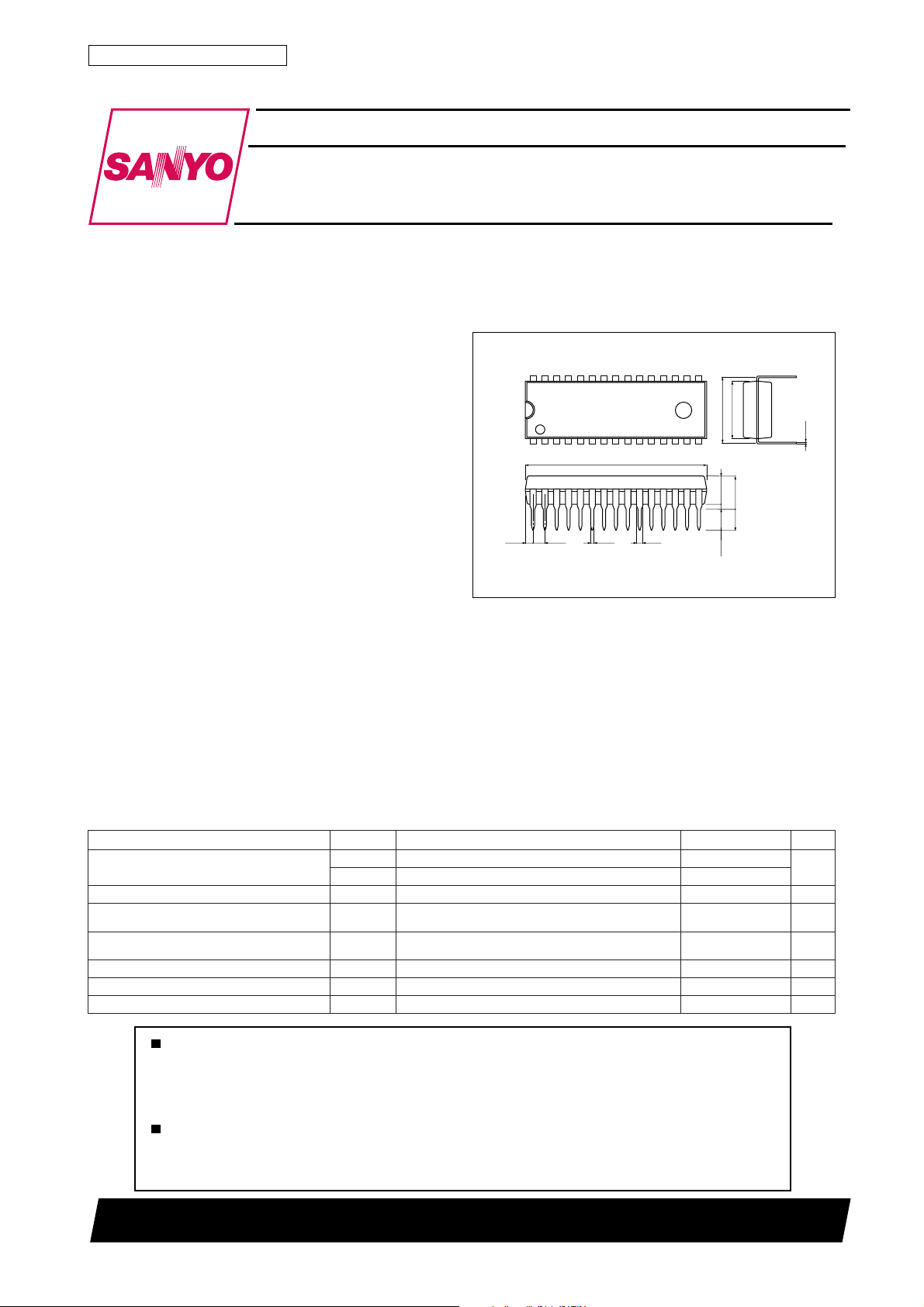
Package Dimensions
unit:mm
3061-DIP30S
[LC7536LHS]
1.15
30
1
1.78
27.2
0.48 0.95
16
15
8.6
10.16
4.25
4.95max
3.2
0.51min
SANYO : DIP30S
0.25
Specifications
Absolute Maximum Ratings at Ta=25˚C, VSS=0V, VEE=0V
retemaraPlobmySsnoitidnoCsgnitaRtinU
V
xam 21ot0
egatlovylppusmumixaM
egnaregatlovtupniECdnaID,KLCV
egnaregatlovtupnigolanAV
egnaregatlovtupniniptceleSV
noitapissidrewopelbawollAxamdPaT ≤ 58°C 052Wm
egnarerutarepmetgnitarepOT
egnarerutarepmetegaortST
DD
V
xam 7ot0
CC
1I
2I
3I
rpo
gts
51501TN (KT)/8051JN No.3942–1/7
V
ot0VCC3.0+V
VEE3.0–
Vot
V
Vot
DD
CC
DD
V
3.0+
3.0–
V
3.0+
˚C
58+ot04–
˚C
521+ot05–
Page 2
LC7536LHS
Recommended Operating Conditions at Ta = 25˚C, VSS = 0 V, VEE = 0 V
retemaraPlobmySsnoitidnoCsgnitaRtinU
egatlovylppusgolanAV
egatlovylppuscigoLV
egatlovylppuscigoLV
Electrical Characteristics at Ta = 25˚C, VCC = 5 V, VDD = 10 V, VEE = 0 V, VSS = 0 V
retemaraPlobmySsnoitidnoC
tnerrucylppuS
egatlovtupnilevel-HGIHsublaireSV
egatlovtupnilevel-HGIHniptceleSV
egatlovtupnilevel-WOLsublaireSV
egatlovtupnilevel-WOLniptceleSV
egatlovtupnIV
htdiwesluptupnIt
emitputeSt
emitdloHt
ycneuqerfgnitarepOf
tnerrucegakaeltuptuOI
noitrotsidcinomrahlatoTDHT
noitcejerklatssorCC
noitaunettamumixaMV
I
I
ΦW
DD
CC
CC
DD
CC
1HI
2HI
1LI
2LI
NI
putes
dloh
gpo
FFO
V
NI
V=RV
r
0
zHk02=f
,VNI
zHk02=f
,VNI
FFOsehctiwsgolanA01–01+Aµ
V,zHk1=f,V3.0=
V–
)xam(R
DD
V1=0657Bd
V1=69Bd
,V01=EE
V
CC
sgnitaR
nimpytxam
V8.0
CC
8.0 ×
V(
DD
V–
)CC
V+
CC
V
SS
V
CC
V
EE
02sµ
02sµ
02sµ
V–
+VCC
220.0%
0.01ot2.3+V
5V
5.5ot6.3V
tinU
1
Am
1
V
V
CC
V
V
DD
V2.0
V
CC
2.0 ×
V(
DD
V
)CC
VDDV
P-P
52zHk
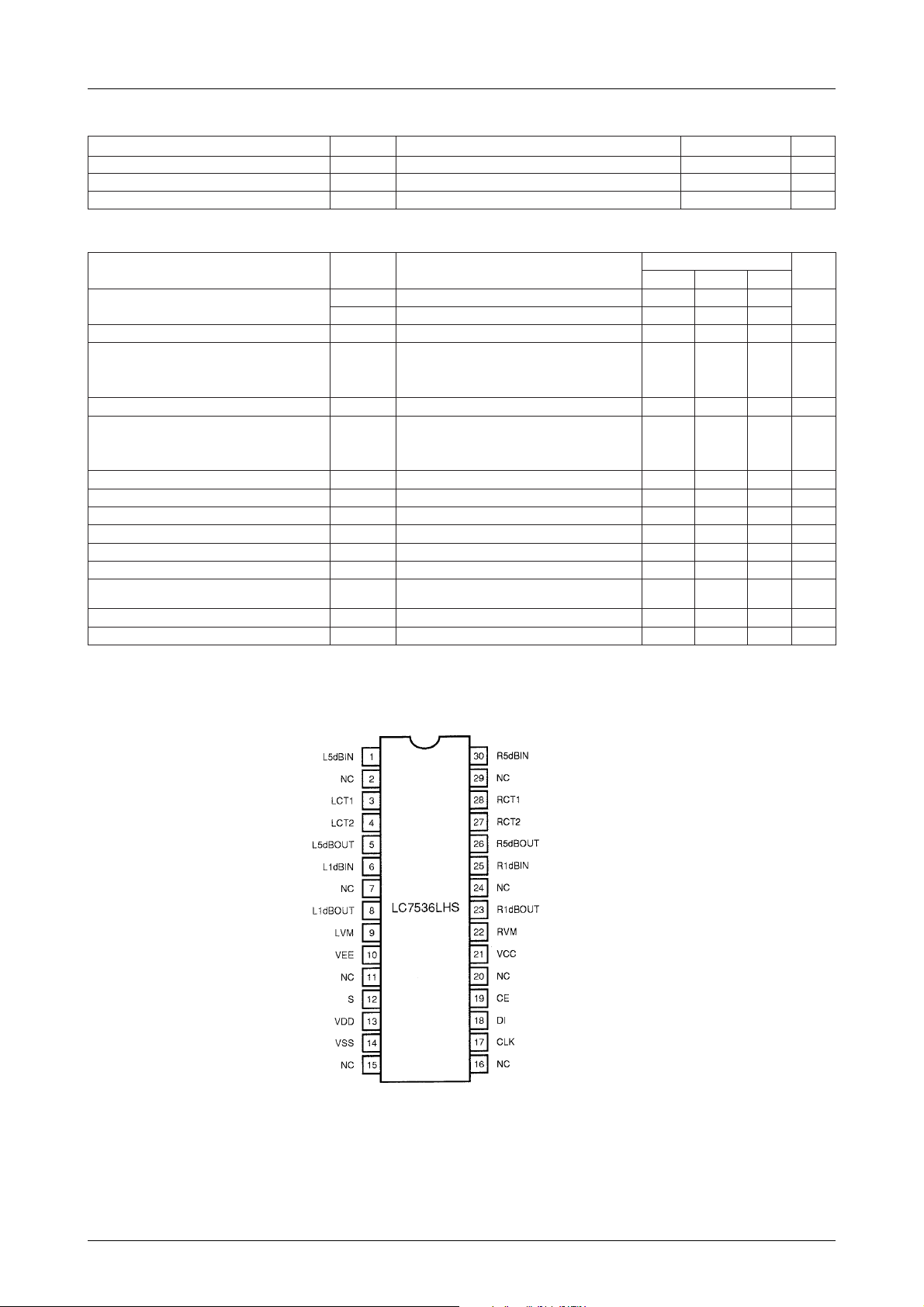
Pin Assignment
Top view
No.3942–2/7
Page 3
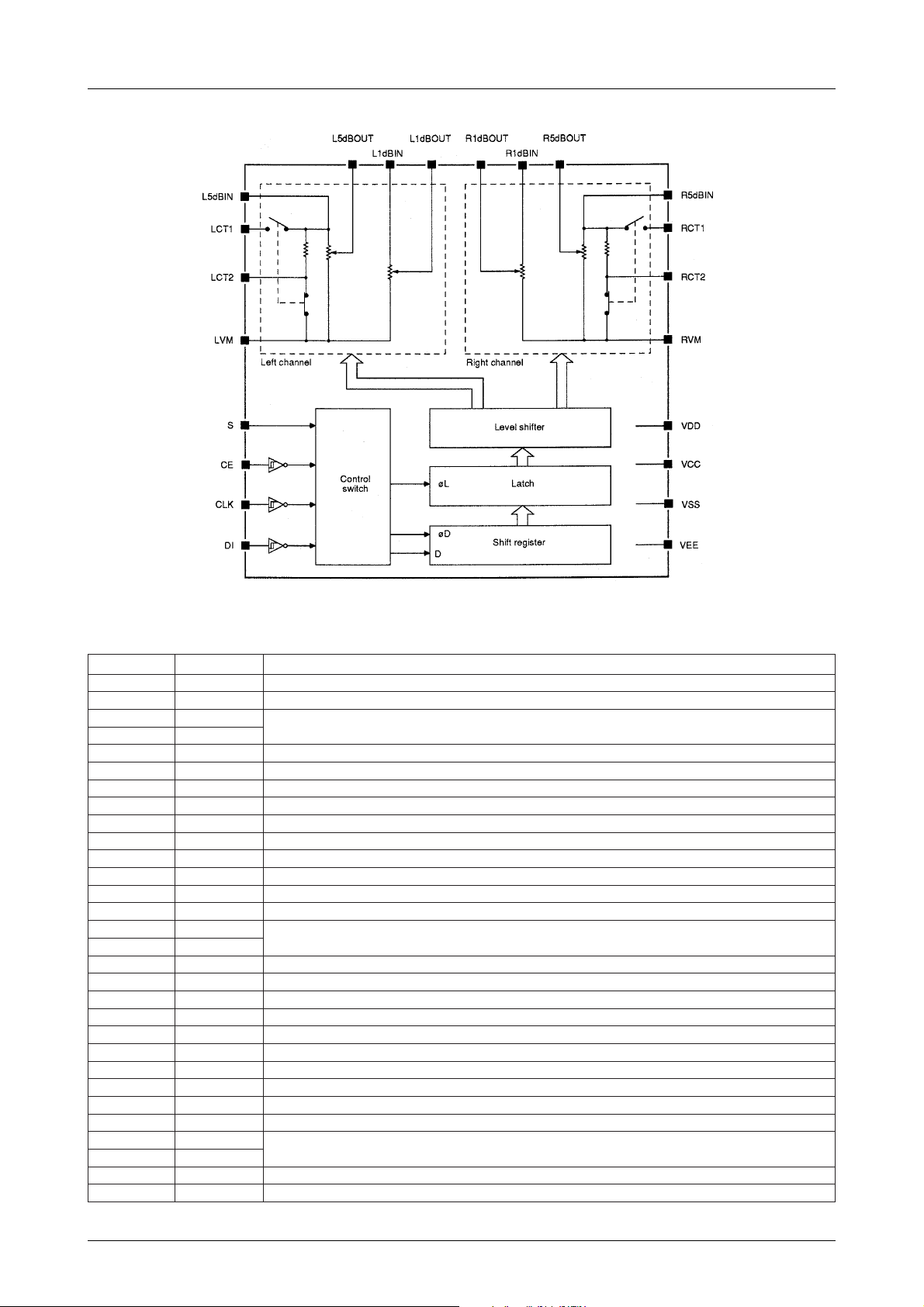
Block Diagram
LC7536LHS
Pin Description
rebmuNemaN noitpircseD
1NIBd5L k57.evirdecnadepmi-woL.tupnipetsnotiatunettaBd5lennahc-tfeL Ω .ecnatsiserlatot
2CNnoitcennocoN
31TCL
42TCL
5TUOBd5L M1yletamixorppA.tuptuopetsnotiatunettaBd5lennahc-tfeL Ω .ecnatsiserdaol
6NIBd1L .evirdecnadepmi-woL.tupnipetsnotiatunettaBd1lennahc-tfeL
7CNnoitcennocoN
8TUOBd1Lk74.tuptuopetsnotiatunettaBd1lennahc-tfeL Ω M1ot Ω .ecnatsiserdaol
9MVL .dnuorgotdetcennocyllamroN.nommoclortnocemulovlennahc-tfeL
01VEEdnuorG
11CNnoitcennocoN
21S .tupnitcelessserddA
31VDDylppusV01
41VSSdnuorG
51CN
61CN
71KLC.tupnikcolC
811D.tupniatadlaireS
91EC.tupnielbanepihC
02CNnoitcennocoN
12VCCylppusV5
22MVR .dnuorgotdetcennocyllamroN.nommoclortnocemulovlennahc-thgiR
32TUOBd1Rk74.tuputopetsnotiatunettaBd1lennahc-thgiR Ω M1ot Ω .ecnatsiserdaol
42CNnoitcennocoN
52NIBd1R .evirdecnadepmi-woL.tupnipetsnotiatunettaBd1lennahc-thgiR
62TUOBd5R M1yletamixorppA.tuptuopetsnotiatunettaBd5lennahc-thgiR Ω .ecnatsiserdaol
722TCR
821TCR
92CNnoitcennocoN
03NIBd5R k57.evirdecnadepmi-woL.tupnipetsnotiatunettaBd5lennahc-thgiR Ω .ecnatsiserlatot
noitcennocoN
.stupninoitasnepmocssenduollennahc-tfeL
.stupninoitasnepmocssenduollennahc-thgiR
No.3942–3/7
Page 4

Timing
LC7536LHS
Functional Description
Data Control
Data is clocked into a 20-bit shift register. When 20 bits
have been receiv ed, the data is latched and then passed to a
level shifter.
Figure 1. Data format
Data Format
The 20-bit data word comprises a 4-bit address code, two
4-bit 5 dB attenuation step selectors, two 3-bit 1 dB attenuation step selectors and a loudness control ON/OFF bit as
shown in figure 1.
No.3942–4/7
Page 5

LC7536LHS
The voltage on the select input determines the address of
the device as shown in table 1.
Table 1. Address codes
niptceleS0A1A2A3A
V
DD
V
CC
1001
0001
Data bits D0 to D3 select the right-channel attenuation in 5
dB steps as shown in table 2. Similarly, bits D8 to D11
select the left-channel attenuation in 5 dB steps.
Table 2. Right-channel 5 dB steps
)Bd(noitaunettA0D1D2D3D
0 1111
5 0111
01 1011
51 0011
02 1101
52 0101
03 1001
53 0001
04 1110
54 0110
05 1010
55 0010
06 1100
56 0100
07 1000
57 0000
Data bits D4 to D6 select the right-channel attenuation in 1
dB steps as shown in table 3. Similarly, bits D12 to D14
select the left-channel attenuation in 1 dB steps.
Table 3. Right-channel 1 dB steps
)Bd(noitaunettA4D5D6D
0011
1101
2001
3110
4010
∞
000
Data bits D7 selects loudness control. When D7 is 1, loudness control is ON, and when 0, loudness control is OFF.
Audio Signal
The right-channel audio input signal is input on R5dBIN(5
dB attenuation steps). The output, R5dBout, is fed back to
R1dBIN (1 dB attenuation steps). The right-channel audio
output is on R1dBOUT . The left-c hannel audio signal flo w
is identical.
No.3942–5/7
Page 6

T ypical Application
LC7536LHS
Figure 2. Typical application
No.3942–6/7
Page 7

LC7536LHS
Specifications of any and all SANYO products described or contained herein stipulate the performance,
characteristics, and functions of the described products in the independent state, and are not guarantees
of the performance, characteristics, and functions of the described products as mounted in the customer's
products or equipment. To verify symptoms and states that cannot be evaluated in an independent device,
the customer should always evaluate and test devices mounted in the customer's products or equipment.
SANYO Electric Co., Ltd. strives to supply high-quality high-reliability products. However, any and all
semiconductor products fail with some probability. It is possible that these probabilistic failures could
give rise to accidents or events that could endanger human lives, that could give rise to smoke or fire,
or that could cause damage to other property. When designing equipment, adopt safety measures so
that these kinds of accidents or events cannot occur. Such measures include but are not limited to protective
circuits and error prevention circuits for safe design, redundant design, and structural design.
In the event that any or all SANYO products(including technical data,services) described or
contained herein are controlled under any of applicable local export control laws and regulations,
such products must not be exported without obtaining the export license from the authorities
concerned in accordance with the above law.
No part of this publication may be reproduced or transmitted in any form or by any means, electronic or
mechanical, including photocopying and recording, or any information storage or retrieval system,
or otherwise, without the prior written permission of SANYO Electric Co. , Ltd.
Any and all information described or contained herein are subject to change without notice due to
product/technology improvement, etc. When designing equipment, refer to the "Delivery Specification"
for the SANYO product that you intend to use.
Information (including circuit diagrams and circuit parameters) herein is for example only ; it is not
guaranteed for volume production. SANYO believes information herein is accurate and reliable, but
no guarantees are made or implied regarding its use or any infringements of intellectual property rights
or other rights of third parties.
This catalog provides information as of May, 2001. Specifications and information herein are subject to
change without notice.
PS No.3942–7/7
 Loading...