

Page 1
Ordering number : ENN*6270
D2499RM (OT) No. 6270-1/20
Overview
The LC75341 and LC75341M are electronic volume and
tone control systems that provide volume, balance, a 2band equalizer, and input switching functions that can be
controlled from serially transferred data.
Functions
• Volume: 0 dB to –79 dB (in 1-dB steps) and –∞, for a
total of 81 settings.
The volume can be controlled independently in the left
and right channels to implement a balance function.
• Bass boost: Up to +20 dB in 2-dB steps. Peaking
characteristics.
• Treble: ±10 dB in 2-dB steps. Shelving characteristics.
• Selector: One of four sets of left/right inputs can be
selected.
• Input gain: The input signal can be boosted by from
0 dB to +30 dB in 2-dB steps.
Features
• On-chip buffer amplifiers minimize the number of
external components.
• Fabricated in a silicon gate CMOS process to minimize
switching noise from internal switches.
• Built-in analog ground reference voltage generation
circuit.
• All controls can be set from serially transferred data.
Supports the CCB standard.
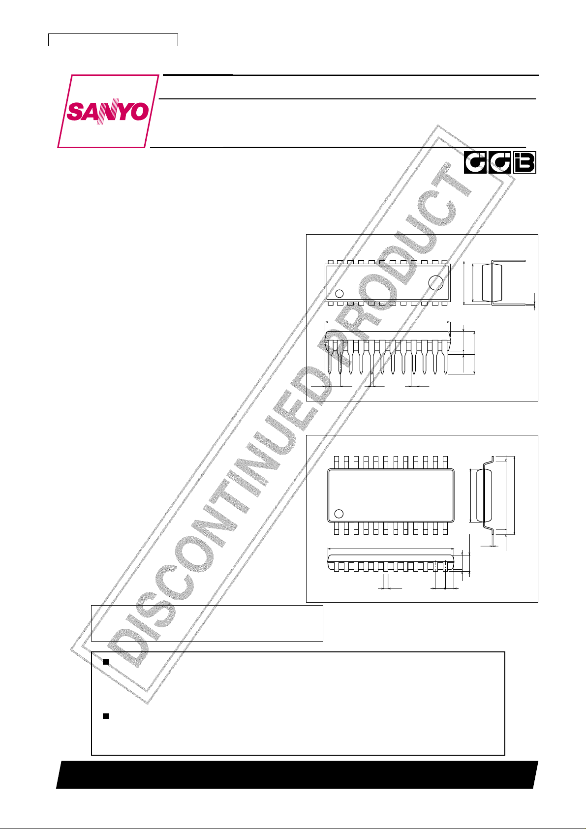
Package Dimensions
unit: mm
3067-DIP24S
unit: mm
3112-MFP24S
0.48
3.25
3.3
3.9max
0.51min
21.2
0.81 1.78
0.25
7.62
6.4
1
12
24
13
0.95
Preliminary
SANYO: DIP24S
[LC75341]
112
24
13
12.6
0.8
1.0
0.15
0.35
5.4
6.35
7.6
0.625
1.8max
1.5
0.1
SANYO: MFP24S
[LC75341M]
LC75341, 75341M
SANYO Electric Co.,Ltd. Semiconductor Company
TOKYO OFFICE Tokyo Bldg., 1-10, 1 Chome, Ueno, Taito-ku, TOKYO, 110-8534 JAPAN
Single-Chip Volume and Tone Control System
CMOS IC
Any and all SANYO products described or contained herein do not have specifications that can handle
applications that require extremely high levels of reliability, such as life-support systems, aircraft’s
control systems, or other applications whose failure can be reasonably expected to result in serious
physical and/or material damage. Consult with your SANYO representative nearest you before using
any SANYO products described or contained herein in such applications.
SANYO assumes no responsibility for equipment failures that result from using products at values that
exceed, even momentarily, rated values (such as maximum ratings, operating condition ranges, or other
parameters) listed in products specifications of any and all SANYO products described or contained
herein.
• CCB is a trademark of SANYO ELECTRIC CO., LTD.
• CCB is a SANYO’s original bus format and all the
bus addresses are controlled by SANYO.
Page 2
No. 6270-2/20
LC75341, 75341M
Specifications
Absolute Maximum Ratings at Ta = 25°C, VSS= 0 V
Parameter Symbol Pin Conditions
Ratings
Unit
min typ max
Supply voltage V
DDVDD
5.0 10 V
High-level input voltage V
IH
CL, DI, CE 2.7 10 V
Low-level input voltage V
IL
CL, DI, CE
7.5 ≤ V
DD
≤ 10.0 V
SS
1.0
V
5.0 ≤ V
DD
< 7.5 V
SS
0.8
Input voltage amplitude V
IN
CE, DI, CL, L1 to L4,
V
SS
V
DD
Vp-p
R1 to R4, LIN, RIN
Input pulse width tøWCL 1 µs
Setup time tsetup CL, DI, CE 1 µs
Hold time thold CL, DI, CE 1 µs
Operating frequency fopg CL 500 kHz
Allowable Operating Ranges at Ta = –30 to +75°C, VSS= 0 V
Parameter Symbol Pin Conditions
Ratings
Unit
min typ max
Input resistance Rin L
IN
, R
IN
50 kΩ
Volume Control Block
Parameter Symbol Pin Conditions
Ratings
Unit
min typ max
Control range Geq max.boost +18 +20 +22 dB
Step resolution Estep 1 2 3 dB
Internal feedback resistance Rfeed 66.6 kΩ
Bass Band Equalizer Control Block
Parameter Symbol Pin Conditions
Ratings
Unit
min typ max
Control range Geq max.boost/cut ±8 ±10 ±12 dB
Step resolution Estep 1 2 3 dB
Internal feedback resistance Rfeed 51.7 kΩ
Treble Band Equalizer Control Block
Electrical Characteristics at Ta = 25°C, V
DD
= 9 V, VSS= 0 V
Input Block
Parameter Symbol Pin Conditions
Ratings
Unit
min typ max
Maximum input gain Gin max +30 dB
Step resolution Gstep +2 dB
Input resistance Rin
L1, L2, L3, L4
50 kΩ
R1, R2, R3, R4
Clipping level Vcl LSEL0, RSEL0 THD = 1.0%, f = 1 kHz 2.90 Vrms
Output load resistance Rl LSEL0, RSEL0 10 kΩ
Parameter Symbol Pin Conditions Ratings Unit
Maximum supply voltage V
DD
max V
DD
11 V
Maximum input voltage V
IN
max
CE, DI, CL, L1 to L4,
VSS– 0.3 to VDD+ 0.3 V
R1 to R4, LIN, RIN
Ta ≤ 75°C LC75341 450
Allowable power dissipation Pdmax
Ta ≤ 75°C
LC75341M 450
mW
with a PCB*
Operating temperature Topr –30 to +75 °C
Storage temperature Tstg –40 to +125 °C
Note: * Printed circuit board size: 76.1 × 114.3 × 1.6 mm, printed circuit board material: glass/epoxy resin
Page 3
No. 6270-3/20
LC75341, 75341M
Parameter Symbol Conditions
Ratings
Unit
min typ max
Total harmonic distortion THD V
IN
= 1 Vrms, f = 1 kHz, all flat overall 0.01 %
Crosstalk CT V
IN
= 1 Vrms, f = 1 kHz, Rg = 1 kΩ, all flat overall 80 dB
Output noise voltage V
N
All flat overall, 80 kHz, L.P.F 9.3 µV
Maximum attenuation Vomin All flat overall, f = 1 kHz –90 dB
Current drain I
DD
VDD– VSS= +10 V 37 mA
High-level input current I
IH
CL, DI, CE: VIN= 10 V 10 µA
Low-level input current I
IL
CL, DI, CE: VIN= 0 V –10 µA
Overall Characteristics
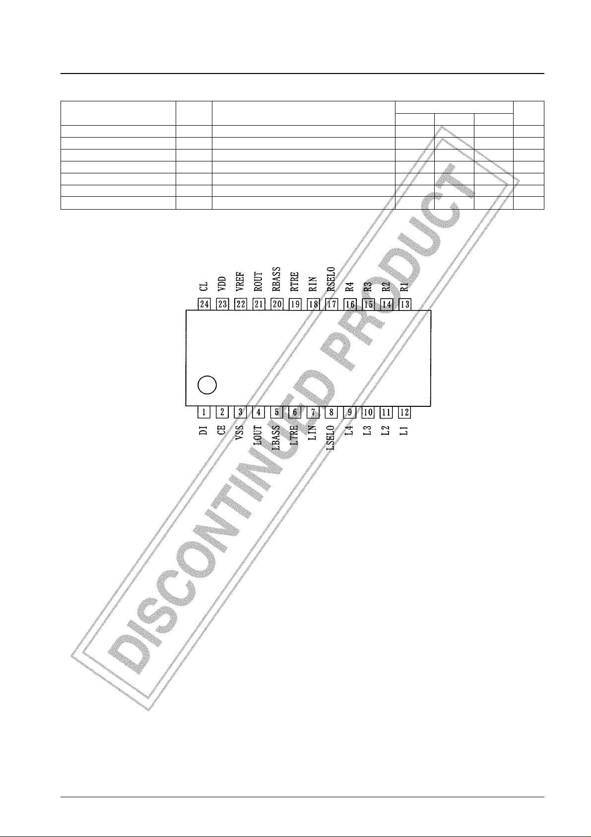
Pin Assignment
(Top view)
LC75341, 75341M
Page 4
No. 6270-4/20
LC75341, 75341M
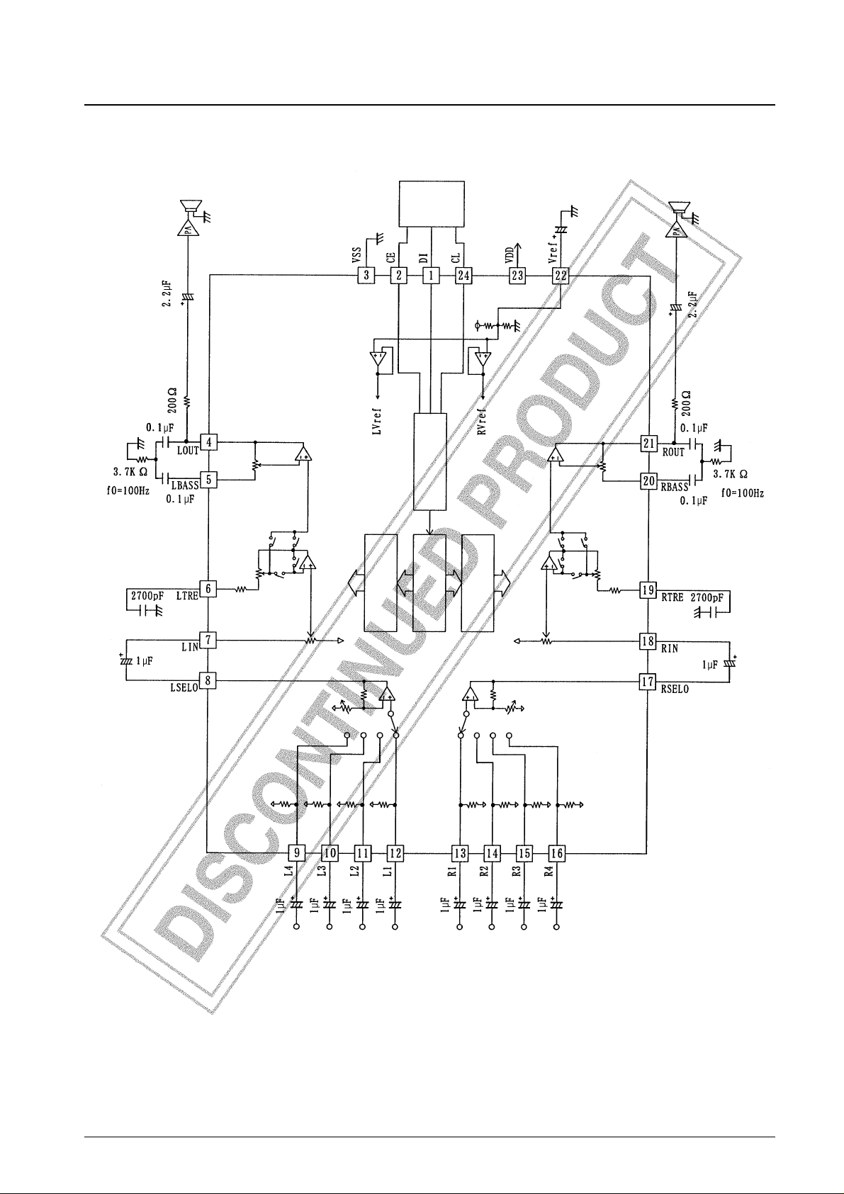
Equivalent Circuit
Control circuit
Logic circuit
CCB interface
Control circuit
Micro-
controller
Page 5
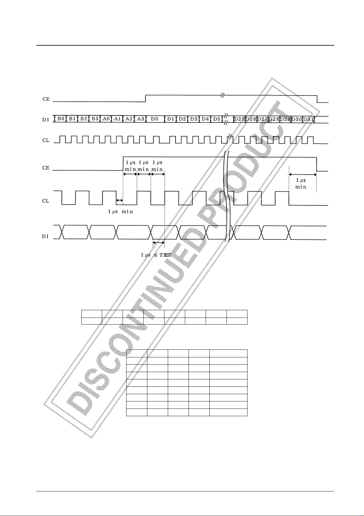
Control System Timing and Data Format
Applications control the LC75341 and LC75341M by applying the stipulated serial data to the CL, DI, and CE pins. This
data consists of a total of 40 bits, of which 8 bits are the address and 32 bits are the data itself.
• Address code (B0 to A3)
The LC75341 and LC75341M have an 8-bit address code, and can be used together with other ICs that support the
Sanyo CCB serial bus format.
Address code
(LSB) (82HEX)
No. 6270-5/20
LC75341, 75341M
B0 B1 B2 B3 A0 A1 A2 A3
01000001
• Control code allocation
Input switching control
(L1, L2, L3, L4, R1, R2, R3, R4)
D0 D1 D2 D3 Operation
0 0 0 0 L1 (R1) ON
1 0 0 0 L2 (R2) ON
0 1 0 0 L3 (R3) ON
1 1 0 0 L4 (R4) ON
0 0 1 0 All switches off
1 0 1 0 All switches off
0 1 1 0 All switches off
1 1 1 0 All switches off
Page 6
No. 6270-6/20
LC75341, 75341M
Input Gain Control
D4 D5 D6 D7 Operation
0000 0 dB
1 0 0 0 +2 dB
0 1 0 0 +4 dB
1 1 0 0 +6 dB
0 0 1 0 +8 dB
1 0 1 0 +10 dB
0 1 1 0 +12 dB
1 1 1 0 +14 dB
0 0 0 1 +16 dB
1 0 0 1 +18 dB
0 1 0 1 +20 dB
1 1 0 1 +22 dB
0 0 1 1 +24 dB
1 0 1 1 +26 dB
0 1 1 1 +28 dB
1 1 1 1 +30 dB
Page 7
No. 6270-7/20
LC75341, 75341M
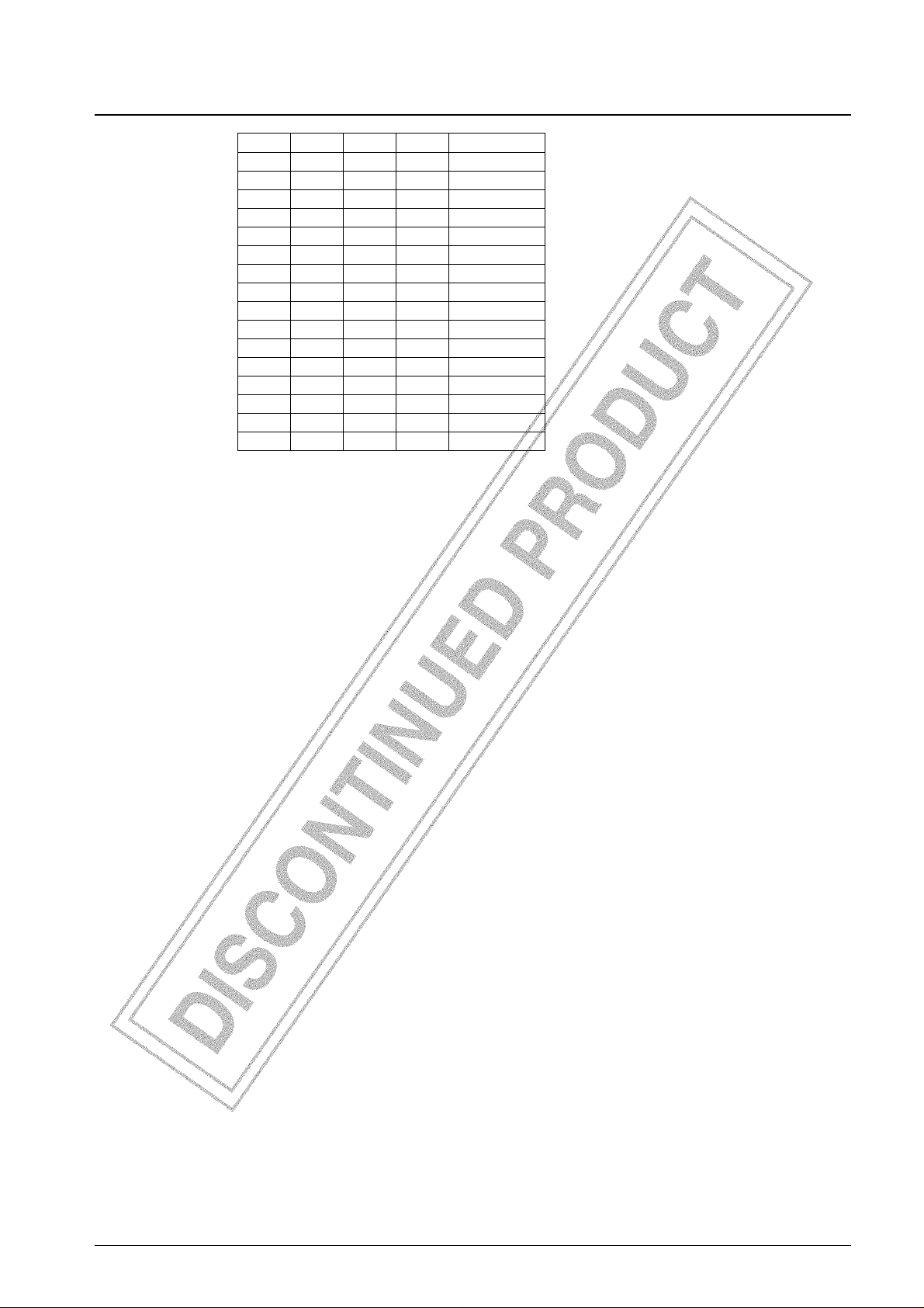
Volume Control
D8 D9 D10 D11 D12 D13 D14 D15 Operation
00000000 0 dB
10000000 –1 dB
01000000 –2 dB
11000000 –3 dB
00100000 –4 dB
10100000 –5 dB
01100000 –6 dB
11100000 –7 dB
00010000 –8 dB
10010000 –9 dB
01010000 –10 dB
11010000 –11 dB
00110000 –12 dB
10110000 –13 dB
01110000 –14 dB
11110000 –15 dB
00001000 –16 dB
10001000 –17 dB
01001000 –18 dB
11001000 –19 dB
00101000 –20 dB
10101000 –21 dB
01101000 –22 dB
11101000 –23 dB
00011000 –24 dB
10011000 –25 dB
01011000 –26 dB
11011000 –27 dB
00111000 –28 dB
10111000 –29 dB
01111000 –30 dB
11111000 –31 dB
00000100 –32 dB
10000100 –33 dB
01000100 –34 dB
11000100 –35 dB
00100100 –36 dB
10100100 –37 dB
01100100 –38 dB
11100100 –39 dB
00010100 –40 dB
10010100 –41 dB
01010100 –42 dB
11010100 –43 dB
00110100 –44 dB
10110100 –45 dB
01110100 –46 dB
11110100 –47 dB
00001100 –48 dB
10001100 –49 dB
01001100 –50 dB
Page 8
No. 6270-8/20
LC75341, 75341M
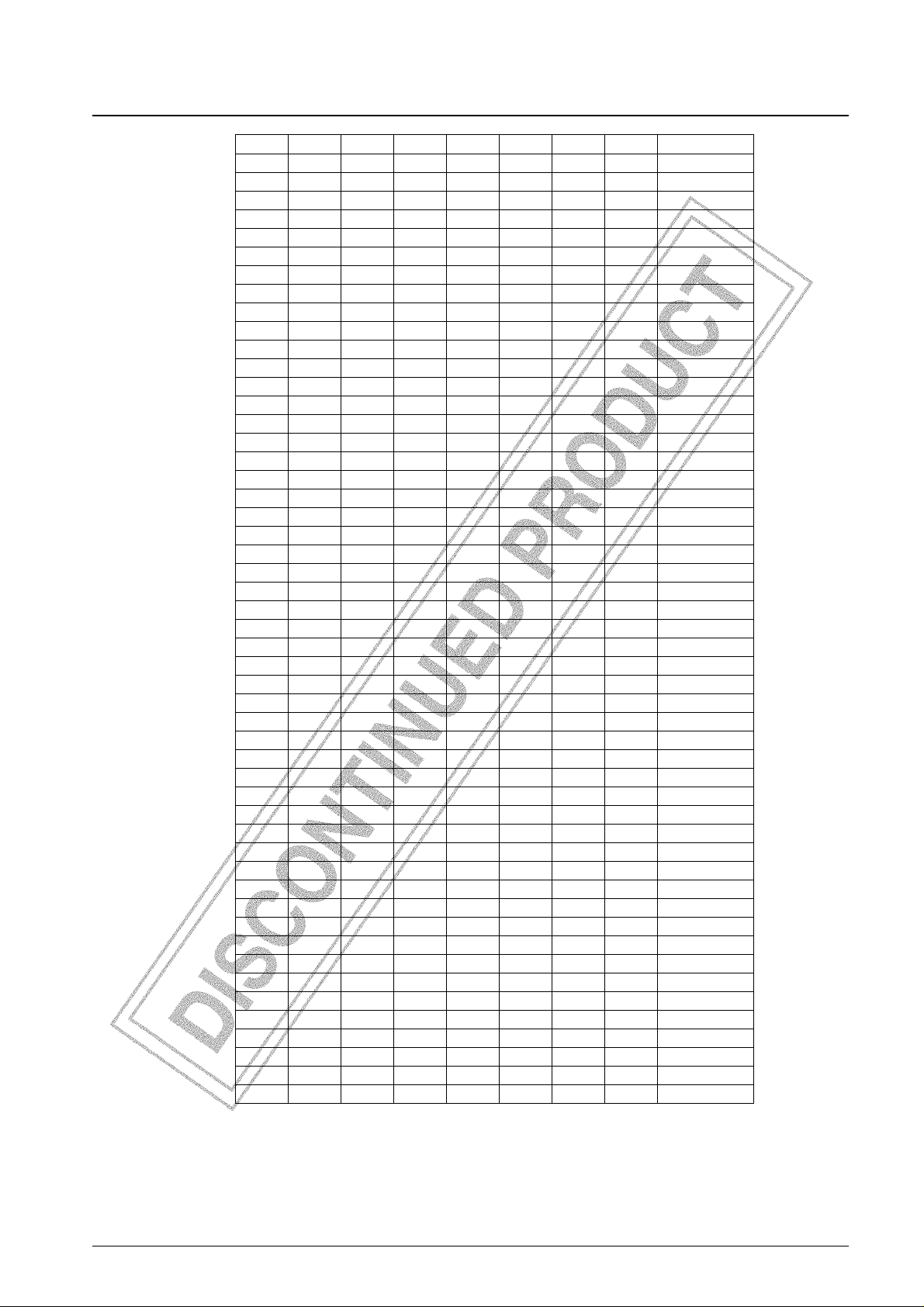
Volume Control
D8 D9 D10 D11 D12 D13 D14 D15 Operation
11001100 –51 dB
00101100 –52 dB
10101100 –53 dB
01101100 –54 dB
11101100 –55 dB
00011100 –56 dB
10011100 –57 dB
01011100 –58 dB
11011100 –59 dB
00111100 –60 dB
10111100 –61 dB
01111100 –62 dB
11111100 –63 dB
00000010 –64 dB
10000010 –65 dB
01000010 –66 dB
11000010 –67 dB
00100010 –68 dB
10100010 –69 dB
01100010 –70 dB
11100010 –71 dB
00010010 –72 dB
10010010 –73 dB
01010010 –74 dB
11010010 –75 dB
00110010 –76 dB
10110010 –77 dB
01110010 –78 dB
11110010 –79 dB
00001010 –∞ dB
Treble Control
D16 D17 D18 D19 Operation
1 0 1 0 +10 dB
0 0 1 0 +8 dB
1 1 0 0 +6 dB
0 1 0 0 +4 dB
1 0 0 0 +2 dB
0000 0 dB
1001 –2 dB
0101 –4 dB
1101 –6 dB
0011 –8 dB
1011 –10 dB
Page 9

No. 6270-9/20
LC75341, 75341M
Bass Control
D20 D21 D22 D23 D24 D25 Operation
0 1 0 1 0 0 +20 dB
1 0 0 1 0 0 +18 dB
0 0 0 1 0 0 +16 dB
1 1 1 0 0 0 +14 dB
0 1 1 0 0 0 +12 dB
1 0 1 0 0 0 +10 dB
001000 +8 dB
110000 +6 dB
010000 +4 dB
101000 +2 dB
000000 0 dB
Channel Selection
D26 D27 Operation
00
1 0 RCH
0 1 LCH
1 1 Left and right together
Test Mode
D28 D29 D30 D31 Operation
0000
These bits are used for IC testing and must all be set to 0
during normal operation.
Page 10
No. 6270-10/20
LC75341, 75341M
Pin Functions
Pin No. Pin Description Notes
• Input signal connections
12
11
10
9
13
14
15
16
L1
L2
L3
L4
R1
R2
R3
R4
• Connections for the resistors and capacitors that form the bass band
filters.
5
20
LBASS
RBASS
• These pins are used both as the connections for the resistors and
capacitors that form the bass band filters and as the outputs from the
bass/treble circuits.
4
21
LOUT
ROUT
• Input selector outputs
8
17
LSEL0
RSEL0
• Connections for the capacitors that form the treble band filters.
6
19
LTRE
RTRE
• Connection to the 0.5 × VDDvoltage generator circuit used as the
analog signal ground.
Applications must connect a capacitor of about 10 µF between this pin
and V
SS
to exclude power supply ripple.
22
Vref
7
18
LIN
RIN
• Volume control and equalizer input
Continued on next page.
Page 11
No. 6270-11/21
LC75341, 75341M
Pin No. Pin Description Notes
• Chip enable
Data is written to the internal latch when this pin goes from high to low.
The internal analog switches operate at this point. Data transfer is
enabled when this pin is high.
2CE
• Serial data and clock inputs used for IC control.
1
24
DI
CL
• Ground3
V
SS
• Power supply23
V
DD
Continued from preceding page.
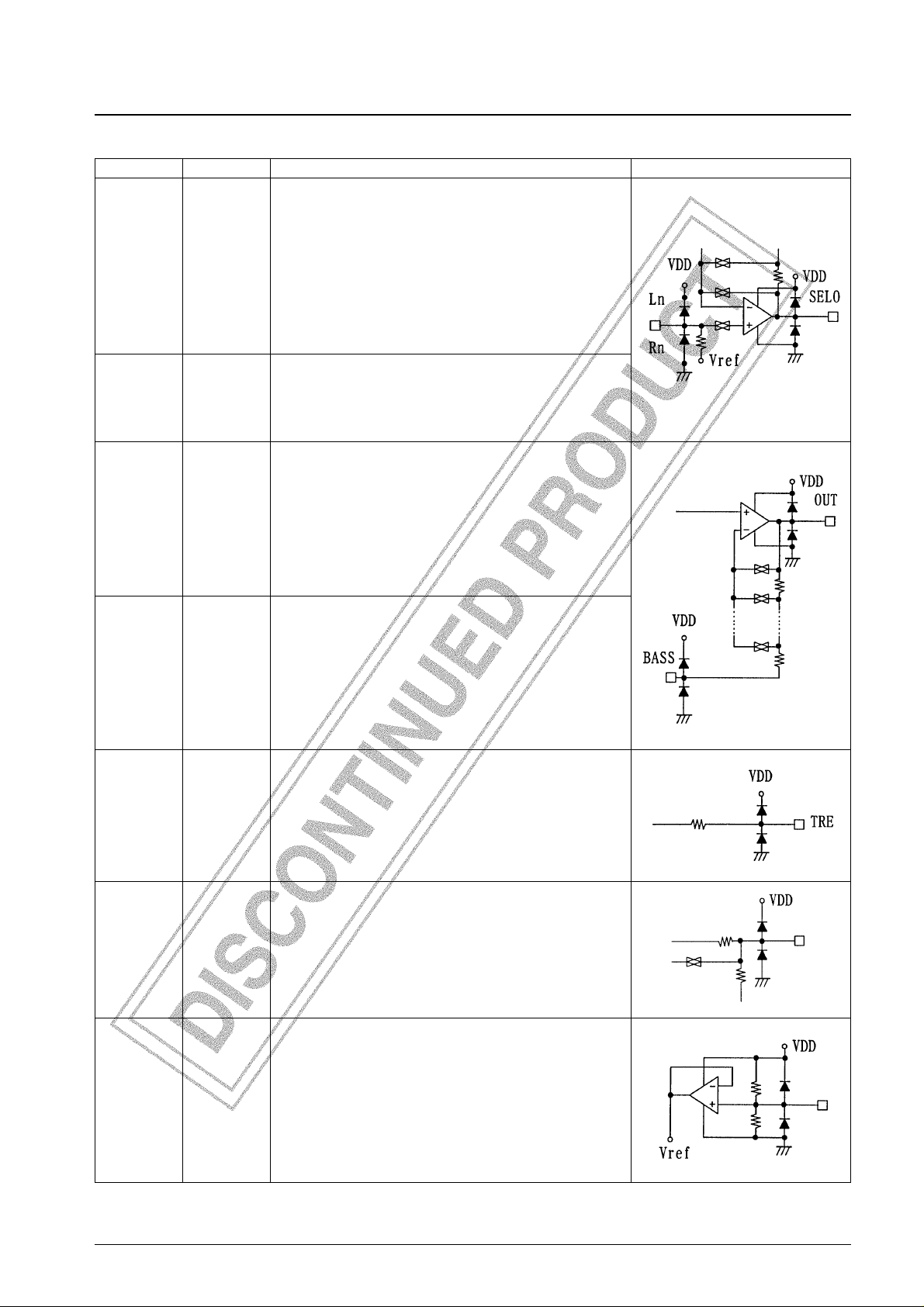
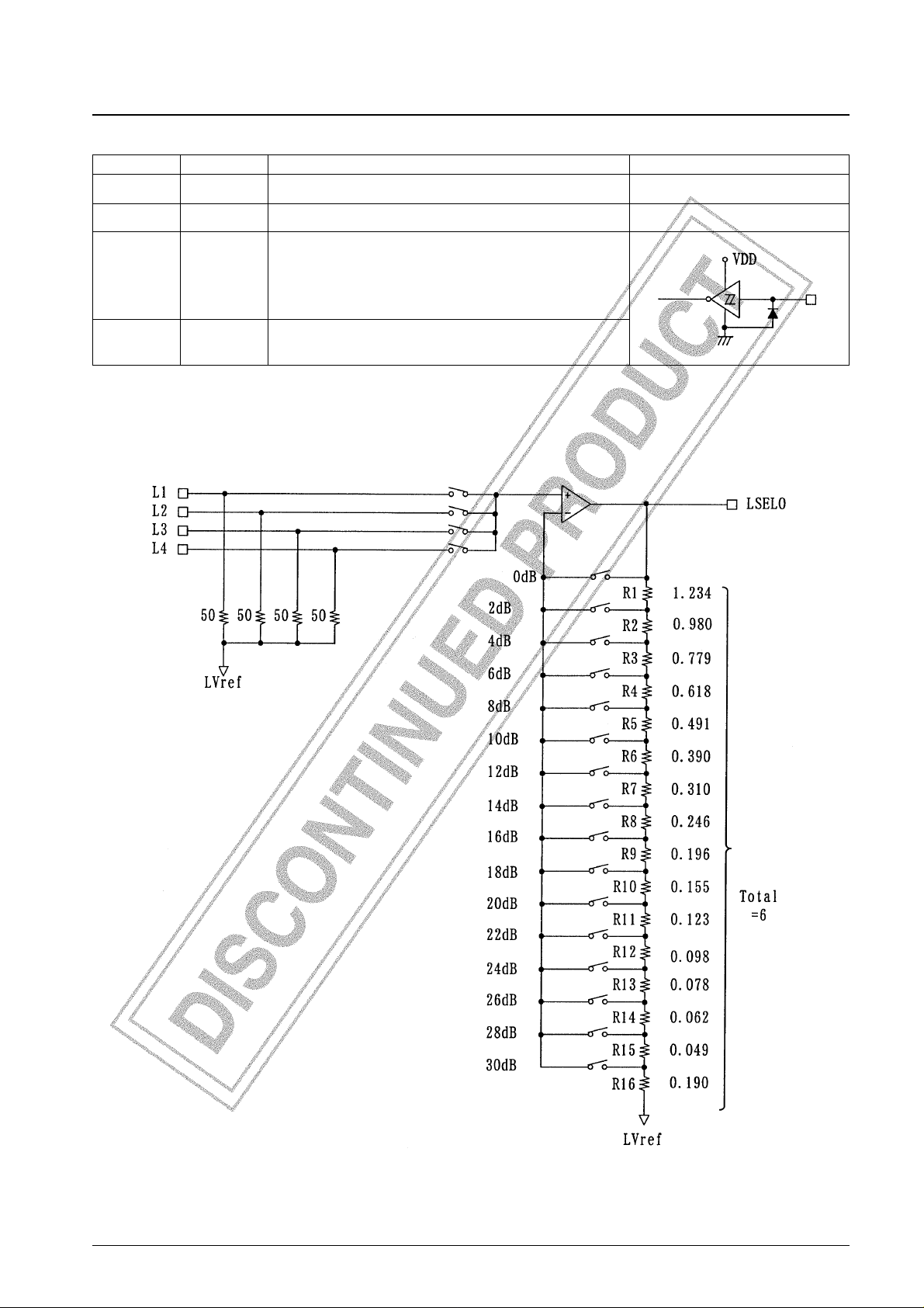
Internal Equivalent Circuits
• Selector block equivalent circuit
The right channel is identical.
Unit (resistance: kΩ)
Page 12

No. 6270-12/20
LC75341, 75341M
• Treble and bass band block internal equivalent circuit
From
volume
block
Set switches SW1 and SW3 to the on position for boost, and set switches SW2 and SW4 to the on
position for cut. For a flat (0 dB) response, set the 0dBSW, SW2, and SW3 switches on.
The right channel is identical.
Unit (resistance: kΩ)
The right channel is identical.
Unit (resistance: kΩ)
Page 13
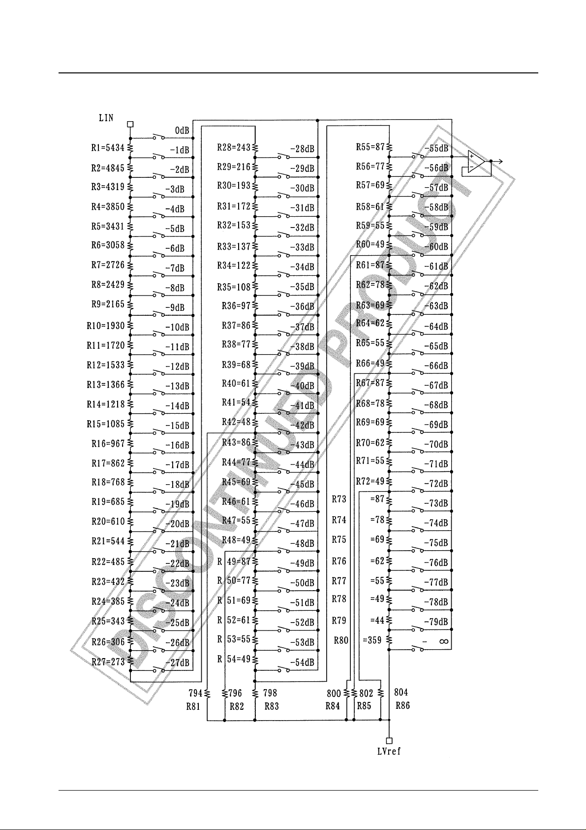
• Volume block internal equivalent circuit
No. 6270-13/20
LC75341, 75341M
To
treble
block
The right channel is identical.
Unit (resistance: Ω)
Page 14

No. 6270-14/20
LC75341, 75341M
Test Circuits
• Total harmonic distortion
The right channel is identical.
Distortion analyzer
Units (resistance: Ω, capacitnace: F)
Microcontroller
LC75341
LC75341M
Page 15

No. 6270-15/20
LC75341, 75341M
• Output noise voltage
The right channel is identical.
Units (resistance: Ω, capacitnace: F)
Noise meter
Microcontroller
LC75341
LC75341M
Page 16

No. 6270-16/20
LC75341, 75341M
• Crosstalk
Units (resistance: Ω, capacitnace: F)
Volt meter
Microcontroller
LC75341
LC75341M
Page 17

Bass Band Circuit
This section presents the equivalent circuit and the calculations for the external capacitors and resistors used to achieve a
center frequency of 100 Hz.
• Bass band equivalent circuit
• Sample calculation
Specifications Center frequency: f0 = 100 Hz
Gain at maximum boost: G = 20 dB
Let R1 = 0, R2 = 66.6 KΩ, and C1 = C2 = C.
(1) Determine R2 from the fact that G = 20 dB.
R2
G
+20dB
= 20 × LOG101 + ——
2R3
R2 66000
R3 = ———————— = ————— ≠3.7 kΩ
2 (10
G+20dB/20
– 1) 2 × (10 – 1)
(2) Determine C from the fact that the center frequency f0 = 100 Hz.
1
f 0 = ————————
2π R3R2C1C2
11
C = —————— = ——————————— ≠ 0.1 µF
2πf 0 R3R22π×100 66000 × 3700
(3) Determine Q.
R3R2 1
Q = ——— • ——— ≠ 2.1
2R3 R3R2
• Treble band circuit
The treble band circuit provides shelving characteristics.
This section presents the equivalent circuit in boost mode and the formulas used to calculate the external component
values.
No. 6270-17/20
LC75341, 75341M
()
Page 18

No. 6270-18/20
LC75341, 75341M
• Sample calculation
Specifications - Set frequency: f = 26,000 Hz
Gain at maximum boost: G
+10dB
= 10 dB
Let R1 = 16.240 kΩ, R2 = 35.461 KΩ,
Substitute the above constants into the following formulas.
R2
G = 20 × LOG
10
1 + ———————
R12+ (1 / ωC)
2
1
C = ———————————
R2
2πf ————— – R1
2
10
G/20
–1
1
= —————————————— ≠ 2700 (pF)
35461
2π26000 ————
2
– 16240
2
3.16 – 1
Usage Notes
• When power is first applied, the states of the internal analog switches will be undefined. Applications must provide
external muting until the control data has been transferred and the switches set to appropriate states.
• Applications should transfer both the left and right channel initial settings data before releasing the muting function
when initializing this IC after first applying power.
• Applications should cover the CL, DI, and CE pin lines with the ground pattern, or should use shielded cables for these
lines to prevent the high-frequency digital signals transmitted over these lines from entering analog signal system.
• When the oscillation occurs, connect a resistor of at least 200 Ω to LOUT and ROUT pins.
()
()
()
Page 19

∞
-100
-90
-80
-70
-60
-50
-40
-30
-20
-10
0
-80 -70 -60 -50 -40 -30 -20 -10 0
-10
10 100 1000 10000 100000
-35
-30
-25
-20
-15
-10
-5
0
10
0.001
0.01
0.1
1
100 1000 10000 100000
10
0.001
0.01
0.1
1
100 1000 10000 100000
0.001
4 5 6 7 8 9 10 11
4 5 6 7 8 9 10 11
0.01
0.1
1
0.001
0.01
0.1
1
0.001
-20 -15 -10 -5 0 5 10
0.01
0.1
1
10
10 100 1000 10000
-30
-25
-20
-15
-10
-5
-0
5
-
No. 6270-19/20
LC75341, 75341M
Step — dB
Volume attenuation — dB
Bass Control Frequency Characteristics
Frequency, f -—Hz
Gain, G — dBV
VDD= 9 V
V
SS
= 0 V
V
IN
= –20 dBV
With external capacitor
and resistor values of
0.1 µF and 3.7 kΩ,
respectively
Treble Control Frequency Characteristics
Frequency, f — Hz
Gain, G — dBV
VDD= 9 V VSS= 0 V
V
IN
= –20 dBV
With an external capacitor
value of 2700 pF
THD - Frequency Characteristics (1)
Total harmonic distortion, THD — %
Frequency, f — Hz
VDD= 9 V
V
SS
= 0 V
V
IN
= 0 dBV
100 kHz low-pass weighting
All tone control settings flat
With the volume
control at the
–10 dB position
With the volume control
at the 0 dB position
VDD= 9 V
V
SS
= 0 V
V
IN
= 0 dBV
f = 1 KHz
All tone control
settings flat
Volume Control Step Characteristics
THD - Frequency Characteristics (2)
Total harmonic distortion, THD — %
Frequency, f — Hz
VDD= 9 V VSS= 0 V
V
IN
= 0 dBV
100 kHz low-pass weighting
All tone control settings flat
With the volume control at the –10 dB position
With the volume control at the 0 dB position
THD - Supply Voltage Characteristics (1)
Total harmonic distortion, THD — %
Supply voltage, VDD— V
VSS= 0 V
V
IN
= 0 dBV
f = 1 KHz
100 kHz low-pass weighting
All tone control settings flat
With the volume control at
the 0 dB position
With the volume control at the –10 dB position
THD - Supply Voltage Characteristics (2)
Total harmonic distortion, THD — %
Supply voltage, VDD— V
VSS= 0 V
V
IN
= –10 dBV
f = 1 KHz
100 kHz low-pass weighting
All tone control settings flat
With the volume control at the –10 dB position
With the volume control at the 0 dB position
THD - Input Level Characteristics (1)
Total harmonic distortion, THD — %
Input level, VIN— dBV
VDD= 9 V
V
SS
= 0 V
100 kHz low-pass
weighting
All tone control settings
flat
f = 20 KHz
f = 1 KHz
Page 20

PS No. 6270-20/20
LC75341, 75341M
This catalog provides information as of December, 1999. Specifications and information herein are
subject to change without notice.
Specifications of any and all SANYO products described or contained herein stipulate the performance,
characteristics, and functions of the described products in the independent state, and are not guarantees
of the performance, characteristics, and functions of the described products as mounted in the customer’s
products or equipment. To verify symptoms and states that cannot be evaluated in an independent device,
the customer should always evaluate and test devices mounted in the customer’s products or equipment.
SANYO Electric Co., Ltd. strives to supply high-quality high-reliability products. However, any and all
semiconductor products fail with some probability. It is possible that these probabilistic failures could
give rise to accidents or events that could endanger human lives, that could give rise to smoke or fire,
or that could cause damage to other property. When designing equipment, adopt safety measures so
that these kinds of accidents or events cannot occur. Such measures include but are not limited to protective
circuits and error prevention circuits for safe design, redundant design, and structural design.
In the event that any or all SANYO products (including technical data, services) described or contained
herein are controlled under any of applicable local export control laws and regulations, such products must
not be exported without obtaining the export license from the authorities concerned in accordance with the
above law.
No part of this publication may be reproduced or transmitted in any form or by any means, electronic or
mechanical, including photocopying and recording, or any information storage or retrieval system,
or otherwise, without the prior written permission of SANYO Electric Co., Ltd.
Any and all information described or contained herein are subject to change without notice due to
product/technology improvement, etc. When designing equipment, refer to the “Delivery Specification”
for the SANYO product that you intend to use.
Information (including circuit diagrams and circuit parameters) herein is for example only; it is not
guaranteed for volume production. SANYO believes information herein is accurate and reliable, but
no guarantees are made or implied regarding its use or any infringements of intellectual property rights
or other rights of third parties.
THD - Input Level Characteristics (1)
Total harmonic distortion, THD — %
Input level, VIN— dBV
V
DD
= 9 V
V
SS
= 0 V
100 kHz low-pass weighting
All tone control settings flat
With the volume control at the
–10 dB position
f = 20 KHz
f = 1 KHz
10
1
0.1
0.01
0.001
-20 -15 -10 -5 0 5 10
 Loading...