

Page 1
Overview
The LC74FCT16245T and LC74FCT162245T 16-bit
transceivers are fabricated in an advanced two-metal-layer
CMOS technology. These fast, low-power transceivers are
optimal for synchronous communication between two
buses, referred to as the A and B busses. The directionality and output enable control in these products is
designed to allow them to be used as either two
independent 8-bit transceivers or as a single 16-bit
transceiver. The direction control pin (× DIR) controls the
data flow direction and the output enable pin (× OE)
disables directionality control and disables both ports.
The LC74FCT16245T is optimal for driving largecapacitance loads and low-impedance loads.
The LC74FCT162245T provides a balanced output drive
function that incorporates current limiting resistors. These
minimize ground bounce and undershoot, and limit the
output fall time. As a result, external series terminating
resistors are no longer required.
The LC74FCT162245T is a plug-in replacement for the
LC74FCT16245T in on-board interface applications.
Features
• 0.8 µm CMOS technology
• Fast, low-power CMOS replacement products for use in
ABT function applications
• ESD tolerance > 2000 V; MIL-STD-883 (when tested
with the 3015 method)
• ESD tolerance > 200 V; For a machine model with C =
200 pF and R = 0 Ω
• Bidirectional data transfer
• 20 mil center SQFP
• Expanded temperature range: –40 to +85°C
•VCC= 5 V ± 10%
LC74FCT16245T Features
• High drive output levels (IOH: –32 mA, IOL: 40 mA)
LC74FCT162245T Features
• Balanced output drive: ±24 mA
• Reduced system switching noise
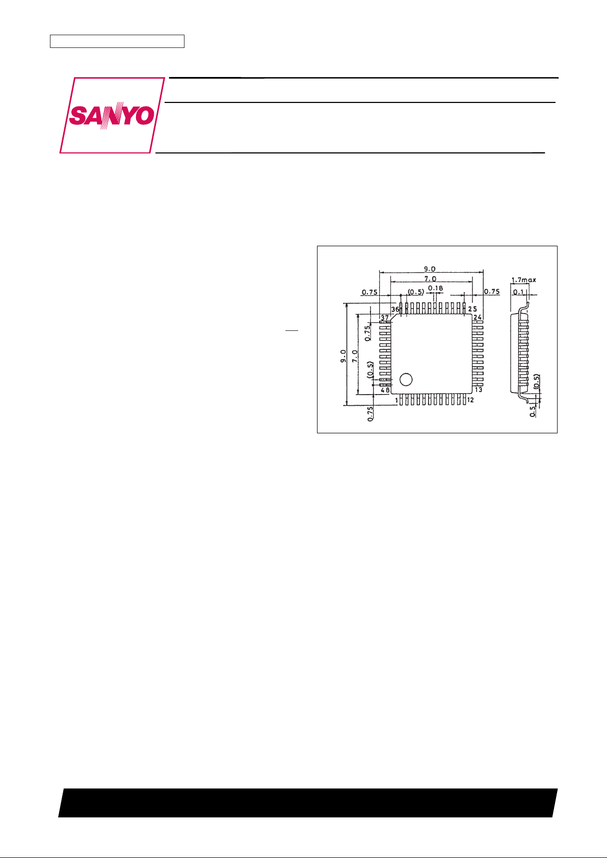
Package Dimensions
unit: mm
3163A-SQFP48
SANYO: SQFP48
[LC74FCT16245T, 74FCT162245T]
CMOS LSI
Ordering number : EN4627
63095HA (OT) No. 4627-1/8
SANYO Electric Co.,Ltd. Semiconductor Bussiness Headquarters
TOKYO OFFICE Tokyo Bldg., 1-10, 1 Chome, Ueno, Taito-ku, TOKYO, 110-8534 JAPAN
Fast 16-Bit CMOS Bidirectional Transceiver
LC74FCT16425T, 74FCT162245T
Page 2
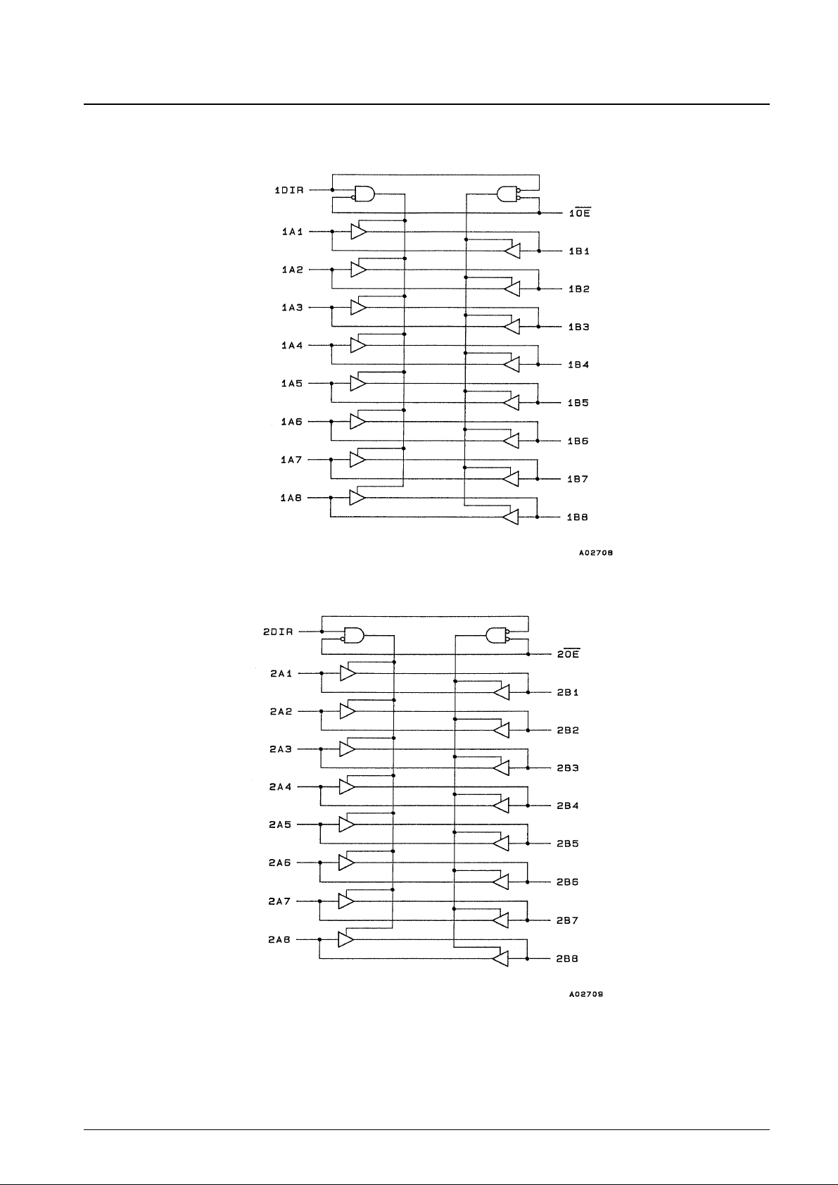
Function Block Diagram
No. 4627-2/8
LC74FCT16245T, 74FCT162245T
Page 3
Pin Functions
Specifications
Absolute Maximum Ratings
*1
Note: 1. Applying stresses in excess of the absolute maximum ratings may permanently damage the device. The values specified here are stress ratings only,
and do not refer to operation under conditions outside either these conditions or the operating conditions. Operating for extended periods at the
absolute maximum ratings may adversely influence device reliability. Unless otherwise specified, pin voltages must not exceed V
CC
+ 0.5 V.
2. All pins except the FCT162xxxT output and I/O pins
3. All FCT162xxxT output and I/O pins
4. See Figure 1.
Function Truth Table*
Note: * H = High level
L = Low level
✕ = Don’t care
Figure 1
Capacitances (Ta = 25°C)
Note: * These capacitance values are logic values, and are not tested.
No. 4627-3/8
LC74FCT16245T, 74FCT162245T
Pin Function
× OE Output enable input (active low)
× DIR Direction control input
× AX A side input or three-state output
× BX B side input or three-state output
Input
Output
× OE × DIR
L L Bus B data output to bus A
L H Bus A data output to bus B
H ✕ High-impedance state.
Parameter Symbol Conditions Ratings Unit
Pin voltage referenced to GND V
TERM
*2
–0.5 to +7.0 V
Pin voltage referenced to GND V
TERM
*3
–0.5 to VCC+ 0.5 V
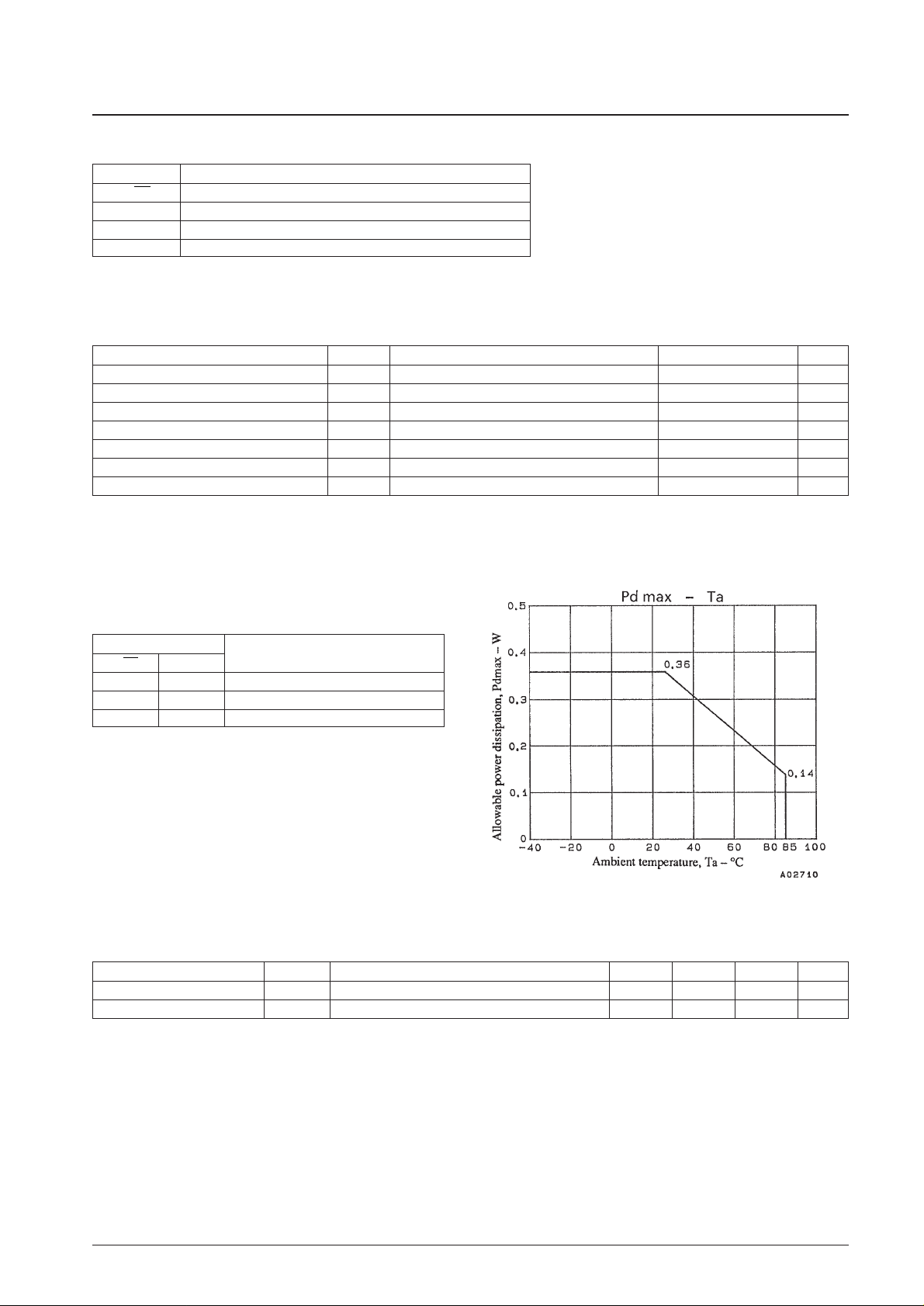
Operating temperature Topr –40 to +85 °C
Temperature when bias is applied T
BIAS
–55 to +125 °C
Storage temperature Tstg –55 to +125 °C
Power dissipation P
T
*4 W
DC output current I
OUT
–60 to +60 mA
Parameter* Symbol Conditions min typ max Unit
Input capacitance C
IN
5.5 8.0 pF
I/O capacitance C
I/O
4.5 6.0 pF
Page 4

DC Electrical Characteristics in the Operating Ranges
The following conditions apply unless otherwise specified.
Ta = –40 to +85°C, VCC= +5.0 V ± 10%
Note: * Values stipulated in the electrical characteristics for the corresponding product must be used for the test conditions for the maximum and minimum
values.
LC74FCT16245T Output Drive Characteristics
Note: 1. Values stipulated in the electrical characteristics for the corresponding product must be used for the test conditions for the maximum and minimum
values.
2. Typical values are values for V
CC
= 5.0 V, and an ambient temperature of +25°C.
3. The test time must not exceed 1 second.
LC74FCT162245T Output Drive Characteristics
Note: 1. Values stipulated in the electrical characteristics for the corresponding product must be used for the test conditions for the maximum and minimum
values.
2. Typical values are values for V
CC
= 5.0 V, and an ambient temperature of +25°C.
3. Do not test more than one output at a time. The test time must not exceed 1 second.
4. The test time must not exceed 1 second.
No. 4627-4/8
LC74FCT16245T, 74FCT162245T
Parameter Symbol Conditions* min typ max Unit
Input high level voltage V
IH
Logic high level guaranteed 2.0 V
Input low level voltage V
IL
Logic low level guaranteed 0.8 V
Input high level current
±5
(input pins)
I
IH
VI= V
CC
Input high level current
±15
(I/O pins)
V
CC
= max µA
Input low level current
±5
(input pins)
I
IL
VI= GND
Input low level current
±15
(I/O pins)
I
CCL
,
Quiescent current I
CCH
, VCC= max, VIN= GND or V
CC
0.05 1.5 mA
I
CCZ
Parameter Symbol Conditions
*1
min typ
*2
max Unit
I
OH
= –3 mA 2.5 3.5 V
Output high level voltage V
OH
VCC= min, VIN= VIHor V
IL
IOH= –15 mA 2.4 3.5 V
I
OH
= –32 mA
*3
2.0 3.0 V
Output low level voltage V
OL
VCC= min, VIN= VIHor V
IL
IOL= 40 mA 0.2 0.55 V
Parameter Symbol Conditions
*1
min typ
*2
max Unit
Output low level current I
ODL
VCC= 5 V, VIN= VIHor VIL, V
OUT
= 1.5 V
*3
60 115 150 mA
Output high level current I
ODH
VCC= 5 V, VIN= VIHor VIL, V
OUT
= 1.5 V
*3
–60 –115 –150 mA
Output high level voltage V
OH
VCC= min, VIN= VIHor V
IL
IOH= –24 mA
*4
2.4 3.3 V
Output low level voltage V
OL
VCC= min, VIN= VIHor V
IL
IOL= 24 mA 0.3 0.55 V
Page 5

Power Supply Current Characteristics
Note: 1. Values stipulated in the electrical characteristics for the corresponding product must be used for the test conditions for the maximum and minimum
values.
2. Typical values are values for V
CC
= 5.0 V, and at an ambient temperature of +25°C.
3. For the TTL drive inputs (V
IN
= 3.4 V), connect all the other inputs to VCCor GND.
4. Although this parameter cannot be directly measured, it is provided for calculating the total power dissipation.
5. The values for these conditions are values with respect to the I
CC
rating. Although these values are guaranteed, they are not tested.
6. I
C
+ I
QUIESCENT
+ I
INPUTS
+ I
DYNAMIC
IC+ ICC+ ∆ICC, DHNT+ I
CCD(fCPNCP
/2 + fiNi)
I
CC
= Quiescent current (I
CCL
, I
CCH
, and I
CCZ
)
∆I
CC
= Supply current for the high-level TTL inputs (VIN= 3.4 V)
D
H
= Duty cycle for the high-level TTL inputs
N
T
= The number of TTL inputs in D
H
I
CCD
= Operating current due to input transition pairs (HLH or LHL)
f
CP
= Clock frequency for register devices (zero for non-register devices)
N
CP
= The number of clocks input in f
CP
fi = Input frequency
Ni = The number of inputs in fi.
LC74FCT16245T/162245T Switching Characteristics in the Operating Ranges
Note: 1. See the figures for the test circuit and waveforms.
2. Although the minimum values are guaranteed, the transmission delay is not tested.
3. Although these items are guaranteed, they are not tested.
4. The skew between two outputs in the same package switched in the same direction. This parameter is a design guarantee.
No. 4627-5/8
LC74FCT16245T, 74FCT162245T
Parameter Symbol Conditions
*1
min typ
*2
max Unit
Quiescent current
∆I
CC
VCC= max, VIN= 3.4 V
*3
0.5 1.5 µA
high-level TTL inputs
V
CC
= max, outputs open,
Operating supply current
*4
I
CCD
× OE = × DIR = GND, VIN= VCC,
100 160 µA/MHz
toggling a single input, V
IN
= GND
50% duty cycle
V
CC
= max, outputs open,
V
IN
= VCC,
0.7 2.5
fi = 10 MHz, × OE = × DIR = GND,
V
IN
= GND
toggling a single bit,
V
IN
= 3.4 V,
0.9 3.3
Total supply current
*6
I
C
50% duty cycle
V
IN
= GND
mA
V
CC
= max, outputs open,
V
IN
= VCC,
2.5 5.5
*
5
fi = 2.5 MHz, × OE = × DIR = GND,
V
IN
= GND
toggling a 16 bits,
V
IN
= 3.4 V,
6.5 17.5
*
5
50% duty cycle
V
IN
= GND
Parameter Symbol Conditions
*1
min typ max Unit
Transmission delay t
PLH
,
1.5 7.0 ns
(From A to B or from B to A) t
PHL
Output enable time t
PZH
*1
,
1.5 12.0 ns
(From × OE to A or B) t
PZL
*1
Output disable time t
PHZ
*1
,
1.5 7.5 ns
(From × OE to A or B) t
PLZ
*1
CL= 50 pF, RL= 500 Ω
Output enable time t
PZH
*2
,
1.5 9.5 ns
(From × DIRS to A or B
*3
) t
PZL
*2
Output disable time t
PHZ
*2
,
1.5 7.5 ns
(From × DIRS to A or B
*3
) t
PLZ
*2
Output skew
*4
tSK(O) 0.5 ns
Page 6

Pin Assignment
Test Circuit and Waveform Diagrams
Test Circuit for All Outputs
Switch Positions
Definitions: CL= Load capacitance: including the jig and probe capacitances
R
T
= Terminating resistance: equivalent to the pulse generator’s Zout.
No. 4627-6/8
LC74FCT16245T, 74FCT162245T
Test Switch
Open drain,
Disable low level, Closed
Enable low level
All other tests Open
Page 7

Setup, Hold, and Release Timing
Transmission Delay
Pulse Width
No. 4627-7/8
LC74FCT16245T, 74FCT162245T
Page 8

PS No. 4627-8/8
LC74FCT16245T, 74FCT162245T
Enable and Disable Timing
Note: 1. These diagrams are for the input enable low level and the input control disable high level cases.
2. Pulse generator setup for all pulses: rate ≤ 1.0 MHz, Zo ≤ 50 Ω, t
f
≤ 2.5 ns, tr≤ 2.5 ns
This catalog provides information as of June, 1995. Specifications and information herein are subject to change
without notice.
■ No products described or contained herein are intended for use in surgical implants, life-support systems, aerospace
equipment, nuclear power control systems, vehicles, disaster/crime-prevention equipment and the like, the failure of
which may directly or indirectly cause injury, death or property loss.
■ Anyone purchasing any products described or contained herein for an above-mentioned use shall:
➀ Accept full responsibility and indemnify and defend SANYO ELECTRIC CO., LTD., its affiliates, subsidiaries and
distributors and all their officers and employees, jointly and severally, against any and all claims and litigation and all
damages, cost and expenses associated with such use:
➁ Not impose any responsibility for any fault or negligence which may be cited in any such claim or litigation on
SANYO ELECTRIC CO., LTD., its affiliates, subsidiaries and distributors or any of their officers and employees
jointly or severally.
■ Information (including circuit diagrams and circuit parameters) herein is for example only; it is not guaranteed for
volume production. SANYO believes information herein is accurate and reliable, but no guarantees are made or implied
regarding its use or any infringements of intellectual property rights or other rights of third parties.
 Loading...