

Page 1

Ordering number : ENN*7023
91801TN (OT) No. 7023-1/14
Overview
The LC74982W is an LCD display scan converter IC that
converts NTSC and PAL TV signals to XGA resolution.
The video signal-processing circuits required to implement
an LCD TV set can be easily formed by combining this IC
with a digital decoder, a microcontroller, and an LCD
panel. Since this IC does not require an external frame
memory for resolution conversion, it can contribute to
minimizing total costs. As additional functionality, it also
provides inputs for personal computer video (up to XGA)
and digital TV (480p/480i). Since LC74982W operation is
based on expansion (resolution increasing) processing,
depending on the input resolution, it can also support use
of, for example, 800 × 600 and 800 × 480 dot resolution
LCD panels. Thus the LC74982W can be used in a wide
range of applications.
Features
•
NTSC and PAL input support: 24-bit or 16-bit digital
YCbCr signal input
• PC input support: Personal computer 24-bit digital RGB
signal input at resolutions up to XGA
• DTV (480i / 480p) input: 24-bit
or 16-bit
digital YCbCr
input
• Two-phase progressive scan RGB 18-bit (24 bit) and 36bit (48 bit) signal output
•
Simulated increased color-depth processing at 6-bit mode.
Values in parentheses apply in 8-bit mode.
•
YCbCr to RGB conversion
• Interlaced to progressive scan conversion
• Resolution conversion (enlargement)
• Variable display size and display position (independently
settable in the horizontal and vertical directions)
• Image quality adjustments: brightness, contrast, color,
sharpness, color phase, black balance, and white balance
• Built-in γ correction (LUT technique. Each 8-bit R, G,
and B signal is independently programmable.)
• Built-in OSD function (8 colors, 253 characters)
•I2C bus interface
• Constant frame-rate processing (identical frame periods
in the input and output signals) adopted so that no
external memory is required.
Specifications
• Supply voltage: 3.3 V (input pins are 5 V tolerant)
• Maximum operating frequency: 65.0 MHz
• Package: SQFP208
Applications
• LCD TVs, monitors, and projectors
• PDP displays
• Car television and car video monitors
Package Dimensions
unit: mm
3210-SQFP208
Preliminary
LC74982W
SANYO Electric Co.,Ltd. Semiconductor Company
TOKYO OFFICE Tokyo Bldg., 1-10, 1 Chome, Ueno, Taito-ku, TOKYO, 110-8534 JAPAN
LCD TV Scan Converter IC
CMOS IC
Any and all SANYO products described or contained herein do not have specifications that can handle
applications that require extremely high levels of reliability, such as life-support systems, aircraft’s
control systems, or other applications whose failure can be reasonably expected to result in serious
physical and/or material damage. Consult with your SANYO representative nearest you before using
any SANYO products described or contained herein in such applications.
SANYO assumes no responsibility for equipment failures that result from using products at values that
exceed, even momentarily, rated values (such as maximum ratings, operating condition ranges, or other
parameters) listed in products specifications of any and all SANYO products described or contained
herein.
28.0
30.6
0.15
0.2
3.8max
0.5
30.6
(0.5)
(1.25)
28.0
1
52
156 105
53
208
104
157
(3.2)
0.35
SANYO: SQFP208
[LC74982W]
Page 2

No. 7023-2/14
LC74982W
I/O Specifications
Input Signal Overview
Signal type Pin No. Pin Description Notes
6 to 13 YIN7 to 0
Y/Y/R
54 to 61 RIN7 to 0
Video signals
16 to 23 UIN7 to 0
C/Cb/G
64 to 71 GIN7 to 0
26 to 33 VIN7 to 0
–/Cr/B
74 to 81 BIN7 to 0
90 HITV NTSC/PAL horizontal sync signal
91 VITV NTSC/PAL vertical sync signal
Sync signals
92 HIDTV DTV horizontal sync signal
93 VIDTV DTV vertical sync signal
94 HIPC PC horizontal sync signal
95 VIPC PC vertical sync signal
96 BLKIH Horizontal enable
Data enable signals
97 BLKIV Vertical enable
36 CLKITV NTSC/PAL clock
Pixel clocks
39 CLKIDTV DTV clock
42 CLKIPC PC clock
167 XTAL Display clock
• NTSC, PAL, and DTV (480i and 480p) inputs
YCbCr signals conform to the CCIR 601 standard.
The YC C signal is a multiplexed CbCr signal
(4:2:2).
• PC input (up to XGA)
• Three independent systems for both horizontal
and vertical sync signals
• Any input polarity may be used. Internal
automatic-discrimination.
• Input with the same logic. The polarity can be
inverted internally.
• A composite video signal can be input to BLKIH.
(BLKIV must be tied high in this case.)
• Three independent input systems
• Fixed frequency crystal oscillator (65 MHz maximum)
Output Signal Overview
Signal type Pin No. Pin Description Notes
106 to 111 ROEVEN5 to 0 Even pixels, red
114 to 119 GOEVEN5 to 0 Even pixels, green
Video signals 122 to 127 BOEVEN5 to 0 Even pixels, blue
in 6-bit output mode 130 to 135 ROODD5 to 0 Odd pixels, red
138 to 143 GOODD5 to 0 Odd pixels, green
146 to 151 BOODD5 to 0 Odd pixels, blue
106 to 111,
ROEVEN7 to 0 Even pixels, red
114, 115
116 to 119,
GOEVEN7 to 0 Even pixels, green
122 to 125
Video signals 126, 127,
BOEVEN7 to 0 Even pixels, blue
in 8-bit output mode 130 to 135
138 to 143,
ROODD7 to 0 Odd pixels, red
146, 147
182 to 189 GOODD7 to 0 Odd pixels, green
192 to 199 BOODD7 to 0 Odd pixels, blue
Sync signals
162 HOUT Horizontal sync signal
163 VOUT Vertical sync signal
Data enable signals
102 BLKHOUT Horizontal enable
103 BLKVOUT Vertical enable
154 DCLK1 Single-phase clock
Pixel clocks
155 DCLK1B Single-phase clock (inverted)
158 DCLK2 Two-phase clock
159 DCLK2B Two-phase clock (inverted)
• Each of the RGB channels is an 6-bit 2-phase
signal.
• The output mode can be switched to single-phase
output mode.
(Output from the ODD pin)
• Each of the RGB channels is an 8-bit 2-phase
signal.
• The output mode can be switched to single-phase
output mode.
(Output from the ODD pin)
• The sync period, position, and polarity can be set.
•
A composite sync signal can be output from VOUT.
• Outputs the same frequency as that of the crystal
oscillator.
• The enable period and the polarity can be set.
•
A composite signal can be output from BLKVOUT.
• Outputs a frequency 1/2 that of the crystal
oscillator.
Page 3

No. 7023-3/14
LC74982W
Control Signal Overview
Signal type Pin No. Pin Description Notes
172 AICS Chip select
Three-wire bus 173 AIDA Data bus
174 AICK Bus clock
175 SDA Data bus
I
2
C-bus
176 SCL Bus clock
• Used for OSD control and γ correction
characteristics settings.
• Used to set the internal control registers and to
output internal status information.
• The slave address is “0111000+ (R/W)”.
Parameter Symbol Conditions Ratings Unit
Maximum supply voltage V
DD
max –0.3 to +4.6 V
Input voltage V
I
–0.5 to + 5.5 V
Output voltage V
O
–0.3 to VDD+ 0.3 V
Allowable power dissipation Pd max Ta = 70°C 0.9 W
Storage temperature Tstg –55 to +125 °C
Operating temperature Topr –30 to +70 °C
Specifications
Absolute Maximum Ratings at VSS= 0 V
Parameter Symbol Conditions
Ratings
Unit
min typ max
Supply voltage V
DD
3.0 3.3 3.6 V
Input voltage range V
IN
0 — 5.5 V
Allowable Operating Ranges at Ta = –30 to +70°C
Parameter Symbol Conditions
Ratings
Unit
min typ max
Input pins C
IN
f = 1 MHz — — 10 pF
Output pins C
OUT
f = 1 MHz — — 10 pF
Bidirectional pins C
I/O
f = 1 MHz — — 10 pF
I/O Pin Capacitances at Ta = 25°C, VDD= VI= 0 V
Note: While the standard operating temperature is –30 to +70°C, for applications such as automotive applications, it can also be used over the range –40 to
+85°C. Note, however, that the value of the allowable power dissipation differs somewhat between these two cases. Contact your SANYO
representative for details if you need to use this device with the latter (wider) operating temperature range.
Parameter Symbol Conditions
Ratings
Unit
min typ max
Input high-level voltage V
IH
CMOS level 0.7 V
DD
— — V
CMOS level Schmitt 0.75 V
DD
— — V
Input low-level voltage V
IL
CMOS level — — 0.2 V
DD
V
CMOS level Schmitt — — 0.15 V
DD
V
Input high-level current I
IH
VI= V
DD
–10 — +10 µA
V
I
= VDD, with pull-down resistors attached. 10 — 100 µA
Input low-level current I
IL
VI= V
SS
–10 — +10 µA
Type B4, I
OH
= –2 mA VDD– 0.8 — — V
Output high-level voltage V
OH
Type B8, IOH= –4 mA VDD– 0.8 — — V
Type B12, I
OH
= –6 mA VDD– 0.8 — — V
Type B4, I
OL
= 2 mA — — 0.4 V
Output low-level voltage V
OL
Type B8, IOL= 4 mA — — 0.4 V
Type B12, I
OL
= 6 mA — — 0.4 V
Output leakage current I
OZ
In the high-impedance output state –10 — +10 µA
Pull-down resistance R
DN
35 70 140 kΩ
Quiescent current* I
DD
Outputs open, VI= VSSor V
DD
— — 100 µA
DC Characteristics at Ta = –30 to +70°C, VDD= 3.0 to 3.6 V
Note: * Certain of the input pins include built-in pull-down resistors. The quiescent current drain cannot be guaranteed in certain situations due to the
structure of these circuits.
Page 4

No. 7023-4/14
LC74982W
Pin Assignment
160
165
170
175
180
185
190
195
200
205
100
95
90
85
80
75
70
65
60
55
DVDD
BLKVOUT
BLKHOUT
RST
DVSS
DVDD
PLLH
BLKIV
BLKIH
VIPC
HIPC
VIDTV
HIDTV
VITV
HITV
DVSS
DVDD
CLPCR
CLPCB
CLPY
CLPP
DVSS
DVDD
BIN0
BIN1
BIN2
BIN3
BIN4
BIN5
BIN6
BIN7
DVSS
DVDD
GIN0
GIN1
GIN2
GIN3
GIN4
GIN5
GIN6
GIN7
DVSS
DVDD
RIN0
RIN1
RIN2
RIN3
RIN4
RIN5
RIN6
RIN7
DVSS
DVSS
DCLK2
DCLK2B
DVDD
DVSS
HOUT
VOUT
VIRST
DVDD
DVSS
XTAL
DVDD
DVSS
EXCTR
MUTE
AICS
AIDA
AICK
SDA
SCL
PDOWN1
PDOWN2
CLKIO
DVDD
DVSS
TSTOA7 (GOODD0)
TSTOA6 (GOODD1)
TSTOA5 (GOODD2)
TSTOA4 (GOODD3)
TSTOA3 (GOODD4)
TSTOA2 (GOODD5)
TSTOA1 (GOODD6)
TSTOA0 (GOODD7)
DVDD
DVSS
TSTOB7 (BOODD0)
TSTOB6 (BOODD1)
TSTOB5 (BOODD2)
TSTOB4 (BOODD3)
TSTOB3 (BOODD4)
TSTOB2 (BOODD5)
TSTOB1 (BOODD6)
TSTOB0 (BOODD7)
TSTMOD3
TSTMOD2
TSTMOD1
TSTMOD0
TSTSUB3
TSTSUB2
TSTSUB1
TSTSUB0
DVDD
DVDD
DCLK1B
DCLK1
DVSS
DVDD
BOODD5 (TEST3)
BOODD4 (TEST2)
BOODD3 (TEST1)
BOODD2 (TEST0)
BOODD1 (ROODD7)
BOODD0 (ROODD6)
DVSS
DVDD
GOODD5 (ROODD5)
GOODD4 (ROODD4)
GOODD3 (ROODD3)
GOODD2 (ROODD2)
GOODD1 (ROODD1)
GOODD0 (ROODD0)
DVSS
DVDD
ROODD5 (BOEVEN7)
ROODD4 (BOEVEN6)
ROODD3 (BOEVEN5)
ROODD2 (BOEVEN4)
ROODD1 (BOEVEN3)
ROODD0 (BOEVEN2)
DVSS
DVDD
BOEVEN5 (BOEVEN1)
BOEVEN4 (BOEVEN0)
BOEVEN3 (BOEVEN7)
BOEVEN2 (BOEVEN6)
BOEVEN1 (BOEVEN5)
BOEVEN0 (BOEVEN4)
DVSS
DVDD
GOEVEN5 (GOEVEN3)
GOEVEN4 (GOEVEN2)
GOEVEN3 (GOEVEN1)
GOEVEN2 (GOEVEN0)
GOEVEN1 (ROEVEN7)
GOEVEN0 (ROEVEN6)
DVSS
DVDD
ROEVEN5
ROEVEN4
ROEVEN3
ROEVEN2
ROEVEN1
ROEVEN0
DVSS
DVSS
OSDRIN
OSDGIN
OSDBIN
OSDEN
YIN7
YIN6
YIN5
YIN4
YIN3
YIN2
YIN1
YIN0
DVDD
DVSS
UIN7
UIN6
UIN5
UIN4
UIN3
UIN2
UIN1
UIN0
DVDD
DVSS
VIN7
VIN6
VIN5
VIN4
VIN3
VIN2
VIN1
VIN0
DVDD
DVSS
CLKITV
DVDD
DVSS
CLKIDTV
DVDD
DVSS
CLKIPC
DVDD
SCANMOD
SCANEN
AVSS
PDO
AVDD
AVSS
VCOCNT
VOCORNG
AVDD
157
208
104
53
52
5045403530252015105
105110115120125130135140145150155
1
105
156
LC74982W
(Top view)
* ( ): Values in parentheses apply in 8-bit mode.
Page 5

No. 7023-5/14
LC74982W
Pin Functions
Pin No. Pin
I/O type
Connection Notes
I/O Type
1 DVSS P GND Digital system ground
2 OSDRIN I g74980m03 Caption OSD microcontroller OSD red input (NTSC only)
3 OSDGIN I g74980m03 Caption OSD microcontroller OSD green input (NTSC only)
4 OSDBIN I g74980m03 Caption OSD microcontroller OSD blue input (NTSC only)
5 OSDEN I g74980m03 Caption OSD microcontroller OSD data enable (NTSC only)
6 YIN7 I g74980m03 Digital decoder MSB
7 YIN6 I g74980m03 or Y signal input
8 YIN5 I g74980m03 ADC or
9 YIN4 I g74980m03 or R signal input
10 YIN3 I g74980m03 Digital Interface
11 YIN2 I g74980m03
12 YIN1 I g74980m03
13 YIN0 I g74980m03 LSB
14 DVDD P Power supply Digital system power supply: 3.3 V
15 DVSS P GND Digital system ground
16 UIN7 I g74980m03 Digital decoder MSB
17 UIN6 I g74980m03 or C (CbCr multiplexed) signal input
18 UIN5 I g74980m03 ADC or
19 UIN4 I g74980m03 or Cb signal input
20 UIN3 I g74980m03 Digital Interface or
21 UIN2 I g74980m03 G signal input
22 UIN1 I g74980m03
23 UIN0 I g74980m03 LSB
24 DVDD P Power supply Digital system power supply: 3.3 V
25 DVSS P GND Digital system ground
26 VIN7 I g74980m03 Digital decoder MSB
27 VIN6 I g74980m03 or Cr signal input
28 VIN5 I g74980m03 ADC or
29 VIN4 I g74980m03 or B signal input
30 VIN3 I g74980m03 Digital Interface
31 VIN2 I g74980m03
32 VIN1 I g74980m03
33 VIN0 I g74980m03 LSB
34 DVDD P Power supply Digital system power supply: 3.3 V
35 DVSS P GND Digital system ground
36 CLKITV I g74980m05 Digital decoder TV clock input (data rate)
37 DVDD P Power supply Digital system power supply: 3.3 V
38 DVSS P GND Digital system ground
39 CLKIDTV I g74980m05 PLL DTV clock input
40 DVDD P Power supply Digital system power supply: 3.3 V
41 DVSS P GND Digital system ground
42 CLKIPC I g74980m05 Digital interface PC clock input (data rate)
43 DVDD P Power supply Digital system power supply: 3.3 V
44 SCANMOD I g74980m03 Open Scan test mode
45 SCANEN I g74980m03 Open Scan test enable
46 AVSS P GND Analog system ground
47 PDO O zwp3vpll3 Loop filter Charge pump output (open)
48 AVDD P Power supply Analog system power supply: 3.3 V
49 AVSS P GND Analog system ground
50 VCOCNT I g74100m06 Loop filter VCO control input (Connect to AV
SS
.)
51 VCORNG I g74100m06 Resistor VCO bias resistor input (Connect to AV
SS
.)
52 AVDD P Power supply Analog system power supply: 3.3 V
Continued on next page.
Page 6
No. 7023-6/14
LC74982W
Continued from preceding page.
Pin No. Pin
I/O type
Connection Notes
I/O Type
53 DVSS P GND Digital system ground
54 RIN7 I g74980m03 Digital Decoder MSB
55 RIN6 I g74980m03 or Y signal input
56 RIN5 I g74980m03 ADC or
57 RIN4 I g74980m03 or R signal input
58 RIN3 I g74980m03 Digital Interface
59 RIN2 I g74980m03
60 RIN1 I g74980m03
61 RIN0 I g74980m03 LSB
62 DVDD P Power supply Digital system power supply: 3.3 V
63 DVSS P GND Digital system ground
64 GIN7 I g74980m03 Digital Decoder MSB
65 GIN6 I g74980m03 or C (CbCr multiplexed) signal input
66 GIN5 I g74980m03 ADC or
67 GIN4 I g74980m03 or Cb signal input
68 GIN3 I g74980m03 Digital Interface or
69 GIN2 I g74980m03 G signal input
70 GIN1 I g74980m03
71 GIN0 I g74980m03 LSB
72 DVDD P Power supply Digital system power supply: 3.3 V
73 DVSS P GND Digital system ground
74 BIN7 I g74980m03 Digital Decoder MSB
75 BIN6 I g74980m03 or Cr signal input
76 BIN5 I g74980m03 ADC or
77 BIN4 I g74980m03 or B signal input
78 BIN3 I g74980m03 Digital Interface
79 BIN2 I g74980m03
80 BIN1 I g74980m03
81 BIN0 I g74980m03 LSB
82 DVDD P Power supply Digital system power supply: 3.3 V
83 DVSS P GND Digital system ground
84 CLPP O POB4 ADC Clamp pulse
85 CLPY O POT4 ADC Y clamp level
86 CLPCB O POT4 ADC Cb clamp level
87 CLPCR O POT4 ADC Cr clamp level
88 DVDD P Power supply Digital system power supply: 3.3 V
89 DVSS P GND Digital system ground
90 HITV I g74980m04 TV decoder TV horizontal synchronizing signal input
91 VITV I g74980m04 TV decoder TV vertical synchronizing signal input
92 HIDTV I g74980m04 Digital interface DTV horizontal synchronizing signal input
93 VIDTV I g74980m04 Digital interface DTV vertical synchronizing signal input
94 HIPC I g74980m04 Digital interface PC horizontal sync signal input
95 VIPC I g74980m04 Digital interface PC vertical sync signal input
96 BLKIH I g74980m02 Digital interface Horizontal blanking signal input (composite blanking signal)
97 BLKIV I g74980m02 Digital interface Vertical blanking signal input (Held high in composite mode)
98 PLLH O POB4 PLL PLL internal divider output
99 DVDD P Power supply Digital system power supply: 3.3 V
100 DVSS P GND Digital system ground
101 RST I g74980m01 Initialization circuit System reset (reset to low)
102 BLKHOUT O POB8 LCD module Horizontal data enable
103 BLKVOUT O POB8 LCD module Vertical data enable or composite data enable
104 DVDD P Power supply Digital system power supply: 3.3 V
Continued on next page.
Page 7

No. 7023-7/14
LC74982W
Continued from preceding page.
Pin No. Pin
I/O type
Connection Notes
I/O Type
105 DVSS P GND Digital system ground
106 ROEVEN0 O POB4 LCD module LSB (LSB)
107 ROEVEN1 O POB4 Red signal output (even)
108 ROEVEN2 O POB4
109 ROEVEN3 O POB4 (Red signal output (even))
110 ROEVEN4 O POB4
111 ROEVEN5 O POB4 MSB
112 DVDD P Power supply Digital system power supply: 3.3 V
113 DVSS P GND Digital system ground
114 GOEVEN0 (ROEVEN6) O POB4 LCD module LSB
115 GOEVEN1 (ROEVEN7) O POB4 (MSB)
116 GOEVEN2 (GOEVEN0) O POB4 Green signal output (even) (LSB)
117 GOEVEN3 (GOEVEN1) O POB4
118 GOEVEN4 (GOEVEN2) O POB4
119 GOEVEN5 (GOEVEN3) O POB4 MSB (Green signal output (even))
120 DVDD P Power supply Digital system power supply: 3.3 V
121 DVSS P GND Digital system ground
122 BOEVEN0 (GOEVEN4) O POB4 LCD module LSB
123 BOEVEN1 (GOEVEN5) O POB4 Blue signal output (even)
124 BOEVEN2 (GOEVEN6) O POB4 (MSB)
125 BOEVEN3 (GOEVEN7) O POB4 (LSB)
126 BOEVEN4 (BOEVEN0) O POB4
127 BOEVEN5 (BOEVEN1) O POB4 MSB
128 DVDD P Power supply Digital system power supply: 3.3 V
129 DVSS P GND Digital system ground
130 ROODD0 (BOEVEN2) O POB4 LCD module LSB
131 ROODD1 (BOEVEN3) O POB4 Red signal output (odd) (B signal output (even))
132 ROODD2 (BOEVEN4) O POB4 or
133 ROODD3 (BOEVEN5) O POB4 Red signal single-phase output
134 ROODD4 (BOEVEN6) O POB4
135 ROODD5 (BOEVEN7) O POB4 MSB (MSB)
136 DVDD P Power supply Digital system power supply: 3.3 V
137 DVSS P GND Digital system ground
138 GOODD0 (ROODD0) O POB4 LCD module LSB (LSB)
139 GOODD1 (ROODD1) O POB4 Green signal output (odd)
140 GOODD2 (ROODD2) O POB4 or
141 GOODD3 (ROODD3) O POB4 Green signal single-phase output (Red signal output (odd)
142 GOODD4 (ROODD4) O POB4 or
143 GOODD5 (ROODD5) O POB4 MSB
Red signal single-phase output)
144 DVDD P Power supply Digital system power supply: 3.3 V
145 DVSS P GND Digital system ground
146 BOODD0 (ROODD6) O POB4 LCD module LSB
147 BOODD1 (ROODD7) O POB4 Blue signal output (odd) (MSB)
148 BOODD2 (TEST0) O POB4 or
149 BOODD3 (TEST1) O POB4 (OPEN) Blue signal single-phase output (Test output (Outputs a fixed
150 BOODD4 (TEST2) O POB4 low level.))
151 BOODD5 (TEST3) O POB4 MSB
152 DVDD P Power supply Digital system power supply: 3.3 V
153 DVSS P GND Digital system ground
154 DCLK1 O POB12 LCD module Data clock 1 (for single-phase data output)
155 DCLK1B O POB12 LCD module Inverted data clock 1 (for single-phase data output)
156 DVDD P Power supply Digital system power supply: 3.3 V
Continued on next page.
Page 8

No. 7023-8/14
LC74982W
Continued from preceding page.
Pin No. Pin
I/O type
Connection Notes
I/O Type
157 DVSS P GND Digital system ground
158 DCLK2 O POB12 — Data clock 2 (for two-phase data output)
159 DCLK2B O POB12 — Inverted data clock 2 (for two-phase data output)
160 DVDD P Power supply Digital system power supply: 3.3 V
161 DVSS P GND Digital system ground
162 HOUT O POB8 LCD module Horizontal sync output
163 VOUT O POB8 LCD module
Vertical synchronizing signal output or composite synchronizing
signal output
164 VIRST O POB4 — Crystal oscillator reset
165 DVDD P Power supply Digital system power supply: 3.3 V
166 DVSS P GND Digital system ground
167 XTAL I g74980m01 VCO Crystal oscillator circuit output
168 DVDD P Power supply Digital system power supply: 3.3 V
169 DVSS P GND Digital system ground
170 EXCTR O POB4 — External control output (output controlled over the I
2
C bus)
171 MUTE I g74980m02 Microcontroller Mute control input (mute to low)
172 AICS I g74980m02 Microcontroller 3-wire bus control chip select
173 AIDA I g74980m02 Microcontroller 3-wire bus control bus data
174 AICK I g74980m02 Microcontroller 3-wire bus control bus clock
175 SDA B g74980m06 Microcontroller I
2
C control data
176 SCL I g74980m02 Microcontroller I
2
C control clock
177 PDOWN1 I g74980m01 — Must be tied high during normal operation.
178 PDOWN2 I g74980m01 — Must be tied high during normal operation.
179 CLKI0 O POB12 — Input system clock output
180 DVDD P Power supply Digital system power supply: 3.3 V
181 DVSS P GND Digital system ground
182 TSTOA7 (GOODD0) O POB4 OPEN MSB (LSB)
183 TSTOA6 (GOODD1) O POB4 Test outputs (G signal output (odd)
184 TSTOA5 (GOODD2) O POB4 (LCD module) or
185 TSTOA4 (GOODD3) O POB4 G signal single-phase output)
186 TSTOA3 (GOODD4) O POB4
187 TSTOA2 (GOODD5) O POB4
188 TSTOA1 (GOODD6) O POB4
189 TSTOA0 (GOODD7) O POB4 LSB (MSB)
190 DVDD P Power supply Digital system power supply: 3.3 V
191 DVSS P GND Digital system ground
192 TSTOB7 (BOODD0) O POB4 OPEN MSB (LSB)
193 TSTOB6 (BOODD1) O POB4 Test outputs (B signal output (odd)
194 TSTOB5 (BOODD2) O POB4 (LCD module) or
195 TSTOB4 (BOODD3) O POB4 B signal single-phase output)
196 TSTOB3 (BOODD4) O POB4
197 TSTOB2 (BOODD5) O POB4
198 TSTOB1 (BOODD6) O POB4
199 TSTOB0 (BOODD7) O POB4 LSB (MSB)
200 TSTMOD3 I g74980m03 OPEN Test mode (Must be left open in normal operation.)
201 TSTMOD2 I g74980m03
202 TSTMOD1 I g74980m03
203 TSTMOD0 I g74980m03
204 TSTSUB3 I g74980m03 OPEN Test sub-mode (Must be left open in normal operation.)
205 TSTSUB2 I g74980m03
206 TSTSUB1 I g74980m03
207 TSTSUB0 I g74980m03
208 DVDD P Power supply Digital system power supply: 3.3 V
Page 9
No. 7023-9/14
LC74982W
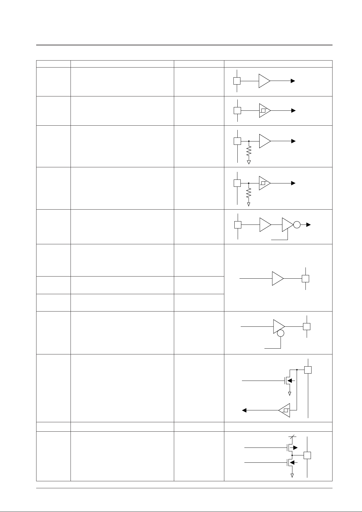
Pin Type
I/O type Applicable pins Function Equivalent circuit
RST
PDOWN1 to 2
XTAL
g74980m01
3 to 5 V voltage
handling input
A13541
AICS, AIDA, AICK
SCL
BLKIH, BLKIV
MUTE
g74980m02
3 to 5 V voltage
handling Schmitt
input
A13542
OSDRIN, OSDGIN, OSDBIN, OSDEN
YIN0 to 7, UIN0 to 7, VIN0 to 7
SCANMOD, SCANEN
RIN0 to 7, GIN0 to 7, BIN0 to 7
TSTMOD0 to 3, TSTSUB0 to 3
Leave open when unused.
g74980m03
3 to 5 V voltage
handling pull-down
input
A13543
HITV, VITV
HIDTV, VIDTV
HIPC, VIPC
g74980m04
3 to 5 V voltage
handling pull-down
Schmitt input
A13544
CLKITV
CLKIDTV
CLKIPC
g74980m05
3 to 5 V voltage
handling OE input
A13545
CLPP, PLLH,
ROEVEN0 to 5 (7), GOEVEN0 to 5 (7), BOEVEN0 to
5 (7), ROODD0 to 5 (7), GOODD0 to 5 (7), BOODD0
to 5 (7), VIRST, EXCTR, TST0A0 to 7, TST0B0 to 7,
(TEST0 to 3)
POB4
4 mA drive output
A13546
A13547
BLKHOUT, BLKVOUT
HOUT, VOUT
POB8 8 mA drive output
DCLK1, DBLK1B, DCLK2, DCLK2B
CLKI0
POB12 12 mA drive output
CLPY, CLPCB, CLPCRPOT4
4 mA 3-state drive
output
A13548
SDAg74980m06
Open-drain I/O
VCOCNT, VCORNGg74100m06 Analog through
PDOzwp3vpll3
Charge pump output
A13549
Note: * All of the DVDD, DVSS, AVDD, and AVSSpins must be connected to the corresponding power or ground level. Do not leave any of these pins open.
Page 10

IC Internal Block Diagram
No. 7023-10/14
LC74982W
6YIN [7 : 0]
RGB
YCbCr
↓ ↓
YCbCr
RGB
G
B
R
8
Y
Cb
Cr
8
Y
Cb
Cr
O
S
D
UIN [7 : 0]
VIN [7 : 0]
13
16 23
26 33
54GIN [7 : 0]
BIN [7 : 0]
RIN [7 : 0]
61
64 71
74 81
106 ROEVEN
When in 8-bit
output mode
6 or 8
GOEVEN
BOEVEN
111
114119
HOUT
VOUT
162
163
BLKHOUT
BLKVOUT
ILC05427
102
103
122127
130 ROODD
GOODD
BOODD
135
138143
146151
106115
116125
126135
138147
182189
192199
90HITV
HIDTV
HIDPC
92
94
91VITV
VIDTV
VIDPC
93
95
96BLKIH
BLKIV
97
CLKITV / CLKIDTV / CLKIPC AICS / AIDA / AICK
DCLK1 / DCLK1B / DCLK2 / DCLK2B
SDA / SCL XTAL
36 39 42 172 173 174 175 167 154 155 158 159176
8
R
G
B
8
R
G
B
Input processing Output processing
Output timing circuit
• Input sync signal detection
• Timing generation for all
horizontal and vertical
timings
Output clock generation circuit
I
2
C bus control
interface
Three-wire bus
control interface
Input clock generation
circuit
Input timing circuit
• Field discrimination
• Horizontal sync signal polarity
discrimination
• Composite blanking signal
discrimination and separation
• Timing generation for all
horizontal and vertical
timings
Color depth processing
γ correction
White balance
Contrast
Black balance
Brightness
Horizontal expansion
Vertical expansion
Expansion processing
Sharpness
Color
phase
Color
Page 11

No. 7023-11/14
LC74982W
Sample Application Circuit (LCD TV/Monitor)
Tuner
Degital
Decoder
LC74982W
TFT-LCD
MODULE
(XGA)
Y (8bit)
CbCr (8bit)
Hsync
Vsync
Pixel clocks
Pixel clocks
Pixel clocks
R (8bit)
G (8bit)
B (8bit)
Hsync
Vsync
PLL
A/DPC
RO (6bit or 8bit)
GO (6bit or 8bit)
BO (6bit or 8bit)
RE (6bit or 8bit)
GE (6bit or 8bit)
BE (6bit or 8bit)
BLK
Hsync
X'Tal
65.0MHz
Microcontroller
LC86F3248A
Vsync
VCR
Page 12
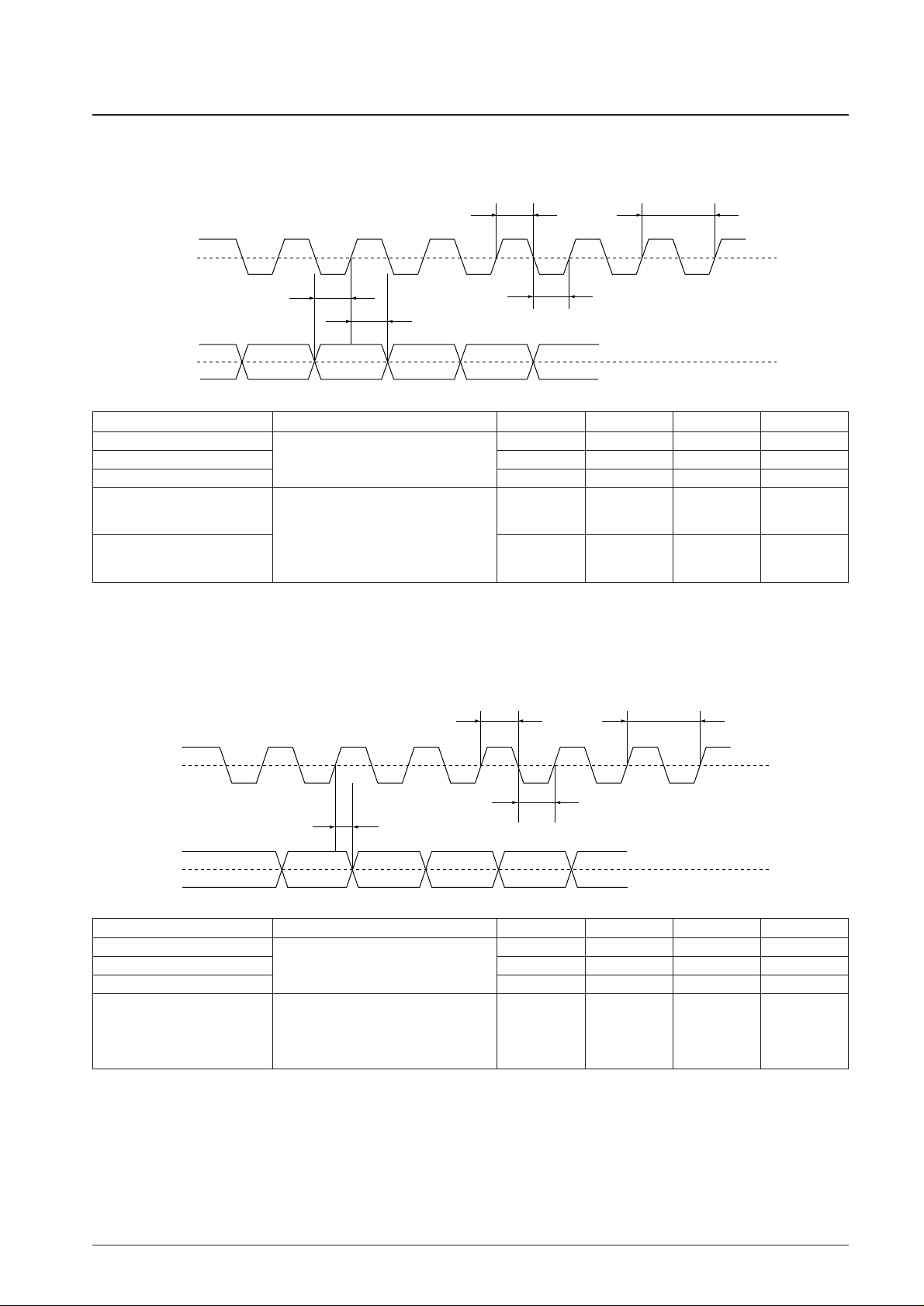
I/O Data Timing
(1) Input data timing
(2) Output data timing
Note: * We recommend using a duty of 50% for the input clock signal.
No. 7023-12/14
LC74982W
t
HI
t
CK
VDD/2
V
DD
/2
t
LO
t
HD
t
SU
Input system
clock
Input data
DCLK2B
Output
data
t
OUT
t
HI
t
CK
t
LO
VDD/2
V
DD
/2
Item Pin Parameter min max Unit
Clock low-level period CLKITV t
LO
7.5 — ns
Clock high-level period CLKIDTV t
HI
7.5 — ns
Clock cycle CLKIPC t
CK
15.0 — ns
YIN [7:0], UIN [7:0]
t
SU
0 — ns
Input data setup time
VIN [7:0], RIN [7:0]
GIN [7:0], BIN [7:0]
Input data hold time
HITV, VITV, HIDTV, VIDTV
t
HD
7.0 — ns
HIPC, VIPC, BLKIH, BLKIV
Item Pin Parameter min max Unit
Clock low-level period t
LO
15.0 — ns
Clock high-level period DCLK2, DCLK2B t
HI
15.0 — ns
Clock cycle t
CK
30.0 — ns
ROEVEN [5(7):0], GOEVEN [5(7):0]
Output data delay time
BOEVEN [5(7):0], ROODD [5(7):0]
t
OUT
0 10 ns
GOODD [5(7):0], BOODD [5(7):0]
BLKHOUT, HOUT, VOUT
Page 13
No. 7023-13/14
LC74982W
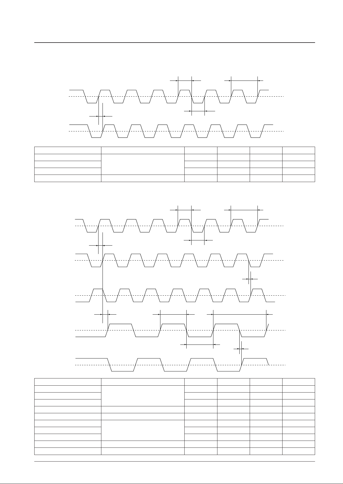
I/O Clock Timing
(1) Input system clock timing
(2) Output system clock timing
CLKITV
CLKIDTV
CLKIPC
CLKIO
t
OUT
t
HI
t
CK
t
LO
VDD/2
V
DD
/2
XTAL
DCLK1
DCLK1B
DCLK2
DCLK2B
t
OUT1
t
LO
t
HI
t
CK
t
D1
t
D2
t
CK2
t
OUT2
t
HI2
t
LO2
VDD/2
V
DD
/2
V
DD
/2
V
DD
/2
V
DD
/2
Item Pin Parameter min max Unit
Clock low-level period CLKITV t
LO
7.5 — ns
Clock high-level period CLKIDTV t
HI
7.5 — ns
Clock cycle CLKIPC t
CK
15.0 — ns
Cock I/O delay time CLKIO t
OUT
5 10 ns
Item Pin Parameter min max Unit
Clock low-level period t
LO
7.5 — ns
Clock high-level period XTAL t
HI
7.5 — ns
Clock cycle t
CK
15.0 — ns
DCLK1 delay time DCLK1 t
OUT1
0 5 ns
DCLK1B delay time DCLK1B t
D1
–1 +1 ns
Clock low-level period t
LO2
15.0 — ns
Clock high-level period DCLK2 t
HI2
15.0 — ns
Clock cycle t
CK2
30.0 — ns
DCLK2 delay time DCLK2 t
OUT2
0 2 ns
DCLK2B delay time DCLK2B t
D2
–1 +1 ns
Page 14

PS No. 7023-14/14
LC74982W
This catalog provides information as of September, 2001. Specifications and information herein are
subject to change without notice.
Specifications of any and all SANYO products described or contained herein stipulate the performance,
characteristics, and functions of the described products in the independent state, and are not guarantees
of the performance, characteristics, and functions of the described products as mounted in the customer’s
products or equipment. To verify symptoms and states that cannot be evaluated in an independent device,
the customer should always evaluate and test devices mounted in the customer’s products or equipment.
SANYO Electric Co., Ltd. strives to supply high-quality high-reliability products. However, any and all
semiconductor products fail with some probability. It is possible that these probabilistic failures could
give rise to accidents or events that could endanger human lives, that could give rise to smoke or fire,
or that could cause damage to other property. When designing equipment, adopt safety measures so
that these kinds of accidents or events cannot occur. Such measures include but are not limited to protective
circuits and error prevention circuits for safe design, redundant design, and structural design.
In the event that any or all SANYO products (including technical data, services) described or contained
herein are controlled under any of applicable local export control laws and regulations, such products must
not be exported without obtaining the export license from the authorities concerned in accordance with the
above law.
No part of this publication may be reproduced or transmitted in any form or by any means, electronic or
mechanical, including photocopying and recording, or any information storage or retrieval system,
or otherwise, without the prior written permission of SANYO Electric Co., Ltd.
Any and all information described or contained herein are subject to change without notice due to
product/technology improvement, etc. When designing equipment, refer to the “Delivery Specification”
for the SANYO product that you intend to use.
Information (including circuit diagrams and circuit parameters) herein is for example only; it is not
guaranteed for volume production. SANYO believes information herein is accurate and reliable, but
no guarantees are made or implied regarding its use or any infringements of intellectual property rights
or other rights of third parties.
 Loading...