


Overview
The LC74786, LC74786M, and LC74786JM are onscreen display controller CMOS ICs that display
characters and patterns on the TV screen under
microprocessor control. These ICs support 12 × 18-dot
characters and can display 12 lines by 24 characters of
text.
Features
• Display format: 24 characters by 12 rows (Up to 288
characters)
• Character format: 12 (horizontal) × 18 (vertical) dots
• Character sizes: Three sizes each in the horizontal and
vertical directions
• Characters in font: 128 (128 characters, one spacing
character, and one transparent spacing character)
• Initial display positions: 64 horizontal positions and 64
vertical positions
• Blinking: Specifiable in character units
• Blinking types: Two periods supported: About 1.0
second and about 0.5 second
• Blanking: Over the whole font (12 × 18 dots)
• Background color: 8 colors (internal synchronization
mode): 2fSCand 4f
SC
• Line background color
— Can be set for 3 lines
— Line background color: 8 colors (internal
synchronization mode): 2fSCand 4f
SC
• External control input: 8-bit serial input format
• On-chip sync separator circuit
• Video outputs - NTSC, PAL, PAL-N, PAL-M, NTSC
4.43, and PAL60 format composite video outputs
• Package
— 24-pin plastic DIP-24S (300 mil)
— 24-pin plastic MFP-24 (375 mil)
— 24-pin plastic MFP-24S (300 mil)
Package Dimensions
unit: mm
3067-DIP24S
unit: mm
3045B-MFP24
unit: mm
3112-MFP24S
CMOS IC
30698HA (OT) No. 5729-1/23
SANYO: DIP24S
[LC74786]
SANYO: MFP24
[LC74786M]
SANYO: MFP24S
[LC74786JM]
SANYO Electric Co.,Ltd. Semiconductor Bussiness Headquarters
TOKYO OFFICE Tokyo Bldg., 1-10, 1 Chome, Ueno, Taito-ku, TOKYO, 110-8534 JAPAN
On-Screen Display Controller
LC74786, 74786M, 74786JM
Ordering number : EN5729A
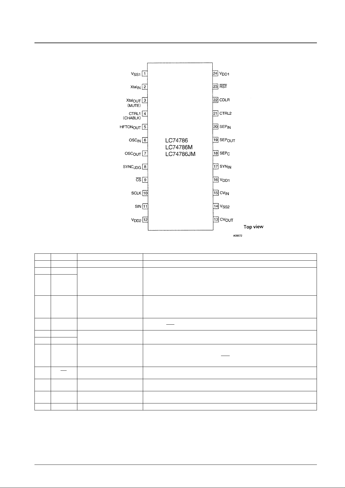
Pin Assignment
No. 5729-2/23
LC74786, 74786M, 74786JM
Pin Functions
Pin No. Pin Name Function Notes
1 V
SS
1 Ground Ground connection (digital system ground)
2 Xtal
IN
These pins are used either to connect the crystal and capacitors used to form an external
Crystal oscillator
crystal oscillator circuit to generate the internal synchronizing signals, or to input an external
Xtal
OUT
(MUTE input)
clock signal (2fsc or 4fsc). As a mask option, the Xtal
OUT
pin can be set to function as the
3
(MUTE) MUTE input pin. When this pin is set low, the video output is held at the pedestal level. (A pull-
up resistor is built in and the input has hysteresis characteristics.)
Switches the mode between external clock input and crystal oscillator operation. A low level
4
CTRL1 Crystal oscillator input switching selects crystal oscillator operation and a high level selects external clock input. As a mask
(CHABLK) (CHABLK output) option, the CTRL1 input pin can be set to function as the CHABLK (character · frame) output.
This is a 3-value output.
5 HFTON
OUT
Background line output
Outputs the range signal specified by LNA*, LNB*, and LNC*. Outputs the crystal oscillator
clock when RST is low. (This signal is not output after a reset command is executed.)
6 OSC
IN
LC oscillator
Connections for the inductor and capacitor that form the character output dot clock generation
7 OSC
OUT
oscillator.
Outputs the state of the external synchronizing signal presence/absence judgment. Outputs a
8 SYNC
JDG
External synchronizing signal high level when synchronizing signals are present.
judgment output Outputs the dot clock (LC oscillator) when RST is low. (This signal is not output on command
resets.)
9 CS Enable input
Serial data input circuit enable pin. Serial data input is enabled when a low level is input.
A pull-up resistor is built in. (This input has hysteresis characteristics.)
10 SCLK Clock input
Serial data input circuit clock input.
A pull-up resistor is built in. (This input has hysteresis characteristics.)
11 SIN Data input
Serial data input.
A pull-up resistor is built in. (This input has hysteresis characteristics.)
12 V
DD
2 Power supply Composite video signal level adjustment power supply (analog system power supply)
Continued on next page.
No. 5729-3/23
LC74786, 74786M, 74786JM
Continued from preceding page.
Pin No. Pin Name Function Notes
13 CV
OUT
Video signal output Composite video signal output
14 V
SS
2 Ground Ground connection (analog system ground)
15 CV
IN
Video signal input Composite video signal input
16 V
DD
1 Power supply Power supply (+5 V: digital system power supply)
Video signal input to the internal sync separator circuit (Used as either the horizontal
17 SYN
IN
Sync separator circuit input synchronizing signal or the composite synchronizing signal input when the internal sync
separator circuit is not used.)
18 SEP
C
Sync separator circuit bias
Internal sync separator circuit bias voltage monitor
voltage
19 SEP
OUT
Composite synchronizing Internal sync separator circuit composite synchronizing signal output. Can be switched to
signal output function as a signal (high, low, or ST. pulse) output by the SEL0 and MOD0 setting.
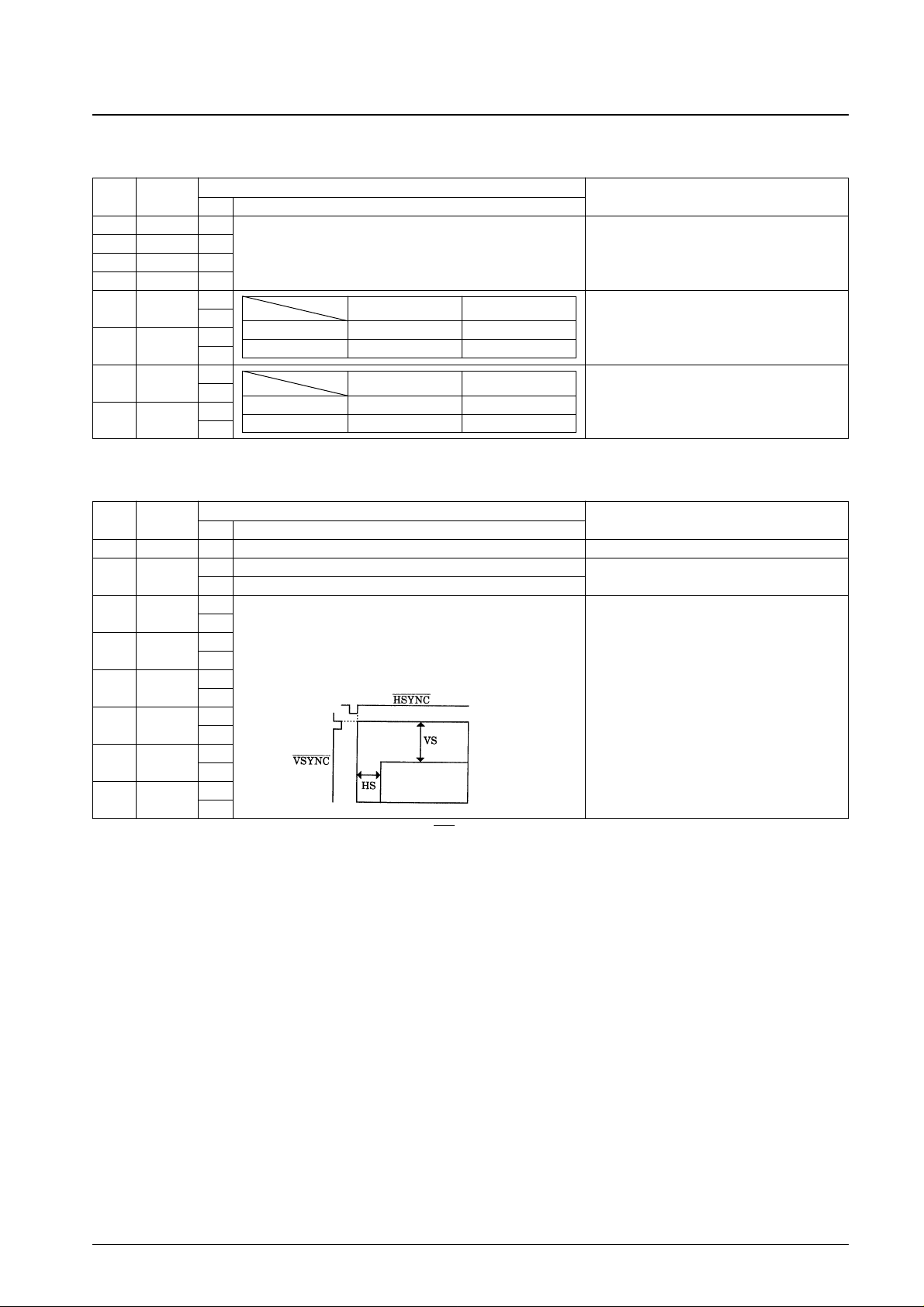
Inputs the vertical synchronizing signal created by integrating the SEP
OUT
pin output signal.
20 SEP
IN
Vertical synchronizing signal input
An integration circuit must be connected to the SEP
OUT
pin. This pin must be tied to VDD1 if
unused. This pin can be switched to function as the frame signal input mode by setting SEL1
high. This is valid when CTL3 is set high. This input has hysteresis characteristics.
Pin settings take priority for switching between the NTSC, PAL, PAL-M, PAL-N, NTSC 4.43,
21 CTRL2 NTSC/PAL-M selection input
and PAL60 video formats. The NTSC format is selected when this pin is low after a reset.
The command video format (NTSC, PAL, PAL-M, PAL-N, NTSC 4.43, or PAL60) selection is
valid. The PAL-M format is selected when this pin is high.
22 CDLR
Background color phase
Background color phase adjustment. Connect a resistor between this pin and ground.
adjustment
23 RST Reset input
System reset input.
A pull-up resistor is built in and the input has hysteresis characteristics.
24 V
DD
1 Power supply (+5 V) Power supply (+5 V: digital system power supply)
Note: Both VDD1 pins must be connected to the power supply.
No. 5729-4/23
LC74786, 74786M, 74786JM
Parameter Symbol Conditions Ratings Unit
Maximum supply voltage V
DD
max VDD1 and VDD2 VSS–0.3 to VS +6.5 V
Maximum input voltage V
IN
max All input pins VS –0.3 to VDD+0.3 V
Maximum output voltage V
OUT
max HFTON
OUT
, SYNC
JDG
, and SEP
OUT
VSS–0.3 to VDD+0.3 V
Allowable power dissipation Pd max Ta = 25°C 350 mW
Operating temperature Topr –30 to +70 °C
Storage temperature Tstg –40 to +125 °C
Specifications
Absolute Maximum Ratings
Parameter Symbol Conditions
Ratings
Unit
min typ max
Supply voltage
V
DD
1 VDD1 4.5 5.0 5.5 V
V
DD
2 VDD2 4.5 5.0 1.27 VDD1 V
Input high-level voltage
V
IH
1 RST, CS, SIN, SCLK, SEPIN, and MUTE 0.8 VDD1 VDD1+0.3 V
V
IH
2 CTRL1 and CTRL2 0.7 VDD1 VDD1+0.3 V
Input low-level voltage
V
IL
1 RST, CS, SIN, SCLK, SEPIN, and MUTE V
SS
– 0.3 0.2 VDD1 V
V
IL
2 CTRL1 and CTRL2 V
SS
– 0.3 0.3 VDD1 V
Pull-up resistance R
PU
RST, CS, SIN, SCLK, and MUTE
25 50 90 kΩ
Applies to pins set up by options.
Composite video signal input voltage
V
IN
1 CVIN: VDD1 = 5 V 2.0 Vp-p
V
IN
2 SYNIN: VDD1 = 5 V 2.0 2.5 Vp-p
Input voltage V
IN
3
Xtal
IN
(when used for external clock input)
0.10 5.0 Vp-p
f
IN
= 2fsc or 4fsc ; VDD1 = 5 V
Xtal
IN
and Xtal
OUT
oscillator pins (2fsc: NTSC) 7.159 MHz
Xtal
IN
and Xtal
OUT
oscillator pins (4fsc: NTSC) 14.318 MHz
Xtal
IN
and Xtal
OUT
oscillator pins (2fsc: PAL) 8.867 MHz
F
OSC
1
Xtal
IN
and Xtal
OUT
oscillator pins (4fsc: PAL) 17.734 MHz
Oscillator frequencies Xtal
IN
and Xtal
OUT
oscillator pins (2fsc: PAL-M) 7.151 MHz
Xtal
IN
and Xtal
OUT
oscillator pins (4fsc: PAL-M) 14.302 MHz
Xtal
IN
and Xtal
OUT
oscillator pins (2fsc: PAL-N) 7.164 MHz
Xtal
IN
and Xtal
OUT
oscillator pins (4fsc: PAL-N) 14.328 MHz
F
OSC
2 OSCINand OSC
OUT
oscillator pins (LC oscillator) 5 10 MHz
Allowable Operating Ranges
Note: Applications must be especially cautious about noise when using the XtalINinput pin in clock input mode.
No. 5729-5/23
LC74786, 74786M, 74786JM
Parameter Symbol Pin Conditions
Ratings
Unit
min typ max
Input off leakage current I
leak1
CV
IN
1 µA
Output off leakage current I
leak2
CV
OUT
1 µA
Output high-level voltage V
OH
1 HFTON
OUT
, SYNC
JDG
, and SEP
OUT
VDD1 = 4.5 V,
3.5 V
I
OH
= –1.0 mA
Output low-level voltage V
OL
1 HFTON
OUT
, SYNC
JDG
, and SEP
OUT
VDD1 = 4.5 V,
1.0 V
I
OL
= –1.0 mA
H 3.3 5.0 V
Three-value output voltage V
O
CHABLK VDD1 = 5.0 V M 1.8 2.3 V
L 0 0.8 V
Input current
I
IH
RST, CS, SIN, SCLK, CTRL1,
V
IN
= VDD1 1 µA
SEP
IN
, and MUTE
I
IL
CTRL1 and OSC
IN
VIN= VSS1 –1 µA
All outputs: open
Operating mode current drain
I
DD
1 VDD1
Xtal:7.159 MHz
15 mA
LC:8 MHz
I
DD
2 VDD2 VDD2 = 5 V 20 mA
(1) 0.70 0.82 0.94
SYNC level V
SN
(2) 0.89 1.01 1.13 V
(3) 1.18 1.30 1.42
(1) 1.32 1.44 1.56
Pedestal level V
PD
(2) 1.52 1.64 1.76 V
(3) 1.81 1.93 2.05
(1) 0.98 1.10 1.22
Color burst low level V
CBL
(2) 1.17 1.29 1.41 V
(3) 1.46 1.58 1.70
(1) 1.63 1.75 1.87
Color burst high level V
CBH
(2) 1.83 1.95 2.07 V
(3) 2.11 2.23 2.35
(1) 1.17 1.29 1.41
Background color low level (other than blue) V
RSL
0 (2) 1.36 1.48 1.60 V
(3) 1.65 1.77 1.89
(1) 2.33 2.45 2.57
Background color high level (other than blue) V
RSH
0 CV
OUT
(2) 2.52 2.64 2.76 V
(1): When the sync level = 0.8 V V
DD
1 = 5.0 V (3) 2.81 2.93 3.05
(2): When the sync level = 1.0 V V
DD
2 = 5.0 V (1) 1.08 1.20 1.32
Blue background 1 low level V
RSL
1 (3): When the sync level = 1.3 V (2) 1.27 1.39 1.51 V
(3) 1.56 1.68 1.80
(1) 1.49 1.61 1.83
Blue background 2 low level V
RSL
2 (2) 1.68 1.80 1.92 V
(3) 1.97 2.09 2.21
(1) 1.97 2.09 2.21
Blue background 1 and 2 high level V
RSH
1, 2 (2) 2.17 2.29 2.41 V
(3) 2.46 2.58 2.70
(1) 1.40 1.52 1.64
Frame level 0 V
BK
0 (2) 1.60 1.72 1.84 V
(3) 1.89 2.01 2.13
(1) 1.97 2.09 2.21
Frame level 1 V
BK
1 (2) 2.17 2.29 2.41 V
(3) 2.46 2.58 2.70
(1) 2.55 2.67 2.79
Character level V
CHA
(2) 2.75 2.87 2.99 V
(3) 3.04 3.16 3.28
Electrical Characteristics at Ta = –30 to +70°C. VDD1 = 5 V unless otherwise specified.
Note: Blue background 1 or 2 are option settings.
No. 5729-6/23
LC74786, 74786M, 74786JM
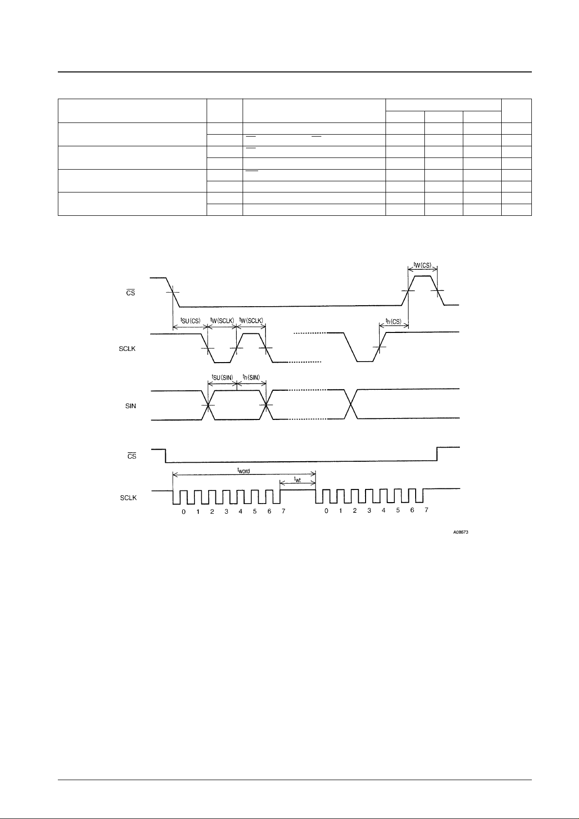
Parameter Symbol Conditions
Ratings
Unit
min typ max
Minimum input pulse width
t
W(SCLK)
SCLK 200 ns
t
W(CS)
CS (The period when CS is high) 1 µs
Data setup time
t
SU(CS)
CS 200 ns
t
SU(SIN)
SIN 200 ns
Data hold time
t
h(CS)
CS 2 µs
t
h(SIN)
SIN 200 ns
One word write time
t
word
The time to write 8 bits of data 4.2 µs
t
wt
The RAM data write time 1 µs
Timing Characteristics at Ta = –30 to +70°C, VDD1 = 5 ±0.5 V
Serial Data Input Timing
First byte
Second byte
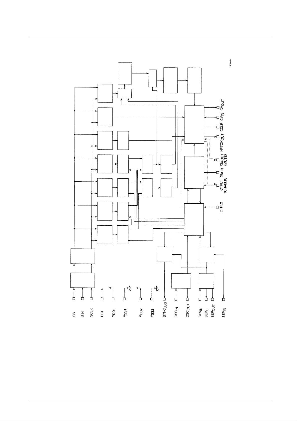
System Block Diagram
No. 5729-7/23
LC74786, 74786M, 74786JM
Serial to
parallel
converter
8-bit
latch +
command
decode
Horizontal
character
size register
Vertical
character
size register
Horizontal
display
position
register
Vertical
display
position
register
Blinking and
reverse
control
register
Display
control
register
RAM write
address
counter
Display
RAM
Deco-
der
Decoder
Font ROM
Shift register
Character output
control
Background control
Video output control
Blinking and
reverse
control circuit
Vertical dot
counter
Horizontal
dot counter
Vertical size
counter
Horizontal
size counter
Vertical display
position
detector
Horizontal
display position
detector
Line control
counter
Character
control
counter
Synchroni-
zation
determination
Composite sync
signal separation
control
Sync
separator
Character
output dot
clock
generator
Sync signal
generator
Timing generator

Display Control Commands
Display control commands have an 8-bit format and are transferred using the serial input function. Commands consist of
a command identification code in the first byte and command data in the following bytes. The following commands are
supported.
1 COMMAND0: Display memory (VRAM) write address setup command
2 COMMAND1: Display character data write command
3 COMMAND2: Vertical display start position and vertical character size setup command
4 COMMAND3: Horizontal display start position and horizontal character size setup command
5 COMMAND4: Display control setup command
6 COMMAND5: Display control setup command
7 COMMAND6: Synchronizing signal detection setup command
8 COMMAND7: Display control setup command
9 COMMAND8: Display control setup command
10 COMMAND9: Display control setup command
11 COMMAND10: Display control setup command
Once written, a first byte command identification code is stored until the next first byte is written. However, when the
display character data write command (COMMAND1) is written, the LC74786/M/JM locks into the display character
data write mode, and another first byte cannot be written.
When the CS pin is set high, the LC74786/M/JM is set to the COMMAND0 (display memory write address setup mode)
state.
No. 5729-8/23
LC74786, 74786M, 74786JM
Display Control Command Table
First byte Second byte
Command
Command identification code
Data Data
7 6 5 4 3 2 1 0 7 6 5 4 3 2 1 0
COMMAND0 1 0 0 0 V3 V2 V1 V0 0 0 0 H4 H3 H2 H1 H0
Write address setup
COMMAND1 1 0 0 1 0 0 0 at c7 c6 c5 c4 c3 c2 c1 c0
Character write
COMMAND2 1 0 1 0 VS VS VS VS 0 FS VP VP VP VP VP VP
Vertical character size and vertical 21 20 11 10 5 4 3 2 1 0
display start position
COMMAND3 1 0 1 1 HS HS HS HS 0 LC HP HP HP HP HP HP
Horizontal character size and 21 20 11 10 5 4 3 2 1 0
horizontal display start position
COMMAND4 1 1 0 0 TST RAM OSC SYS 0 BLK BLK BLK BK BK RV DSP
Display control MOD ERS STP RST 2 1 0 1 0 ON
COMMAND5 1 1 0 1 NP NP NON INT 0 NP 0 BCL CB PH PH PH
Display control 1 0 2 2 1 0
COMMAND6 1 1 1 0 SEL MOD DIS MUT 0 RN RN RN SN SN SN SN
Synchronizing signal detection 0 0 LIN 2 1 0 3 2 1 0
COMMAND7 1 1 1 1 0 0 SEL CTL 0 0 0 VNP VSP MSK MSK EGL
Display control 1 3 SEL SEL ERS SEL
COMMAND8 1 1 1 1 0 1 VSY HSY 0 LNA LNA LNA LNA LPA LPA LPA
Display control SEL SEL 3 2 1 0 2 1 0
COMMAND9 1 1 1 1 1 0 LNB MOD 0 LNB LNB LNB LNB LPB LPB LPB
Display control SEL 2 3 2 1 0 2 1 0
COMMAND10 1 1 1 1 1 1 LNC MOD 0 LNC LNC LNC LNC LPC LPC LPC
Display control SEL 3 3 2 1 0 2 1 0
COMMAND0 (Display memory write address setup command)
No. 5729-9/23
LC74786, 74786M, 74786JM
• First byte
DA
Register
Contents
Notes
0 to 7 State Function
7 — 1
6 — 0 Command 0 identification code.
5 — 0 Sets the display memory write address.
4 — 0
3 V3
0
1
2 V2
0
1
Display memory line address (0 to B hexadecimal)
1 V1
0
1
0 V0
0
1
• Second byte
DA
Register
Contents
Notes
0 to 7 State Function
7 — 1 Second byte identification code
6 — 0
5 — 0
4 H4
0
1
3 H3
0
1
2 H2
0
Display memory column address (0 to 17 hexadecimal)
1
1 H1
0
1
0 H0
0
1
Note: All registers are set to 0 when the LC74786/M/JM is reset by the RST pin.
No. 5729-10/23
LC74786, 74786M, 74786JM
COMMAND1 (Display character data write setup command)
• First byte
DA
Register
Contents
Notes
0 to 7 State Function
7 — 1
6 — 0 Command 1 identification code.
5 — 0 Sets up display character data write mode.
4 — 1
3 — 0
2 — 0
1 — 0
0 at
0 Character attribute off
1 Character attribute on
When this command is input, the LC74786/M/JM
locks in the display character data write mode until
the CS pin goes high.
• Second byte
DA
Register
Contents
Notes
0 to 7 State Function
7 c7
0
1
6 c6
0
1
5 c5
0
1 Character code (00 to 7F hexadecimal)
4 c4
0
1 (FE (hex): spacing character)
3 c3
0 (FF (hex): transparent spacing character)
1
2 c2
0
1
1 c1
0
1
0 c0
0
1
Note: All registers are set to 0 when the LC74786/M/JM is reset by the RST pin.
No. 5729-11/23
LC74786, 74786M, 74786JM
COMMAND2: Vertical display start position and vertical character size setup command
• First byte
DA
Register
Contents
Notes
0 to 7 State Function
7 — 1
6 — 0 Command 2 identification code.
5 — 1 Sets the vertical display start position and the vertical character size.
4 — 0
3 VS21
0
1
Second line vertical character size
2 VS20
0
1
1 VS11
0
1
First line vertical character size
0 VS10
0
1
VS20
0 1
VS21
0 1H/dot 2H/dot
1 3H/dot 1H/dot
The vertical display start position is set by the 6 bits
VP0 to VP5.
The weight of bit 1 is 2H.
• Second byte
DA
Register
Contents
Notes
0 to 7 State Function
7 — 0 Second byte identification bit
6 F
S
0 Crystal oscillator frequency: 2fsc
1 Crystal oscillator frequency: 4fsc
5
VP5 0 If VS is the vertical display start position then:
(MSB) 1 VS = α + H ×(2Σ 2
n
VPn)
4 VP4
0 H: the horizontal synchronization pulse period
1 α= 20 H (in 525-line systems)
3 VP3
0 = 25 H (in 625-line systems)
1
2 VP2
0
1
1 VP1
0
1
0
VP0 0
(LSB) 1
Note: All registers are set to 0 when the LC74786/M/JM is reset by the RST pin.
5
n=0
VS10
0 1
VS11
0 1H/dot 2H/dot
1 3H/dot 1H/dot
Character
display area
No. 5729-12/23
LC74786, 74786M, 74786JM
COMMAND3 (Horizontal display start position and horizontal size setup command)
• First byte
DA
Register
Contents
Notes
0 to 7 State Function
7 — 1
6 — 0 Command 3 identification code.
5 — 1
Sets the horizontal display start position and the horizontal character size.
4 — 1
3 HS21
0
1
Second line horizontal character size
2 HS20
0
1
1 HS11
0
1
First line horizontal character size
0 HS10
0
1
HS20
0 1
HS21
0 1 Tc/dot 2 Tc/dot
1 3 Tc/dot 1 Tc/dot
• Second byte
DA
Register
Contents
Notes
0 to 7 State Function
7 — 0 Second byte identification bit
6 LC
0 Use the LC oscillator for the dot clock
1 Use the crystal oscillator for the dot clock
5
HP5 0 If HS is the horizontal start position then:
(MSB) 1 HS =Tc × (2Σ 2
n
HPn)
4 HP4
0 Tc: Period of the oscillator connected to OSCIN/OSCOUT in operating
1 mode.
3 HP3
0
1
2 HP2
0
1
1 HP1
0
1
0
HP0 0
(LSB) 1
Note: All registers are set to 0 when the LC74786/M/JM is reset by the RST pin.
5
n=0
HS10
0 1
HS11
0 1 Tc/dot 2 Tc/dot
1 3 Tc/dot 1 Tc/dot
The horizontal display start position is set by the 6
bits HP0 to HP5.
The weight of bit 1 is 2Tc.
Selects the dot clock used for character display in the
horizontal direction.

No. 5729-13/23
LC74786, 74786M, 74786JM
COMMAND4 (Display control setup command)
• First byte
DA
Register
Contents
Notes
0 to 7 State Function
7 — 1
6 — 1 Command 4 identification code
5 — 0
Display character data write setup
4 — 0
3 TSTMOD
0 Normal operating mode
This bit must be set to 0.
1 Test mode
2 RAMERS
0
1 Erase display RAM. (The RAM data is set to FF hexadecimal.)
1 OSCSTP
0 Do not stop the crystal and LC oscillators
1 Stop the crystal and LC oscillators
0 SYSRST
0
1 Reset all registers and turn display off
• Second byte
DA
Register
Contents
Notes
0 to 7 State Function
7 — 0 Second byte identification bit
6 BLK2
0 Character display area
Specifies the size for complete fill in
1 Video display area
5 BLK1
0
1
Changes the blanking size
4 BLK0
0
1
3 BK1
0 Blinking period: About 0.5 s
Switches the blinking period
1 Blinking period: About 1.0 s
2 BK0
0 Blinking off
1 Blinking on
1 RV
0 Reverse video off
1 Reverse video on
0 DSPON
0 Character display off
1 Character display on
Note: All registers are set to 0 when the LC74786/M/JM is reset by the RST pin.
Blinking in reverse video mode switches the display between
normal character display and reverse video display
Erasing RAM takes about 500 µs. (This operation
must be executed in the DSPOFF state.)
Valid in external synchronization mode when
character display is off
The registers are reset when the CS pin is low, and
the reset state is cleared when CS is set high
BLK0
0 1
BLK1
0 Blanking off Character size
1 Frame size Complete fill in
No. 5729-14/23
LC74786, 74786M, 74786JM
COMMAND5 (Display control setup command)
• First byte
DA
Register
Contents
Notes
0 to 7 State Function
7 — 1
6 — 1 Command 5 identification code.
5 — 0
Display control setup.
4 — 1
3 NP1
0
1
2 NP0
0
1
1 NON
0 Interlaced
1 Noninterlaced
0 INT
0 External synchronization
1 Internal synchronization
• Second byte
DA
Register
Contents
Notes
0 to 7 State Function
7 — 0 Second byte identification bit
6 NP2
0
Set with NP0 and NP1.
1
5 — 0
4 BCL
0 Background color on
Only valid in internal synchronization mode.
1 No background color (Only the background level is set)
3 CB
0 Color burst signal output
Only valid when BCL is high.
1 Color burst signal output stopped
2 PH2
0
1
1 PH1
0
1
0 PH0
0
1
Note: All registers are set to 0 when the LC74786/M/JM is reset by the RST pin.
Background color specification
Switches between the NTSC, PAL, PAL-N, PAL-M,
NTSC 4.43, and PAL60 formats
Switches between external and internal
synchronization
Switches between interlaced and noninterlaced video
NP2 NP1 NP0 Format
0 0 0 NTSC
0 0 1 PAL-M
0 1 0 PAL
0 1 1 PAL-N
1 0 0 NTSC4.43
1 0 1 PAL60
PH2 PH1 PH0 Background color (phase)
0 0 0 Cyan
0 0 1 Yellow
0 1 0 Red
0 1 1 Blue
1 0 0 Cyan blue
1 0 1 Green
1 1 0 Orange
1 1 1 Magenta

DA
Register
Contents
Notes
0 to 7 State Function
7 — 1
6 — 1 Command 6 identification code.
5 — 1
Sets up synchronizing signal control.
4 — 0
3 SEL0
0
1
2 MOD0
0
1
1 DISLIN
0 12 lines
Switches the number of lines displayed
1 10 lines
0 MUT
0 Normal output
CV
OUT
switching
1 CV
IN
is cut and CV
OUT
is held at the pedestal level
SEL0 MOD SEP
OUT
output
0 0 Sync separator signal
0 1 Low-level output
1 0 High-level output
1 1 ST pulse signal
No. 5729-15/23
LC74786, 74786M, 74786JM
COMMAND6 (Synchronizing signal detection setup command)
• First byte
Switches the SEP
OUT
(pin 19) output
• Second byte
DA
Register
Contents
Notes
0 to 7 State Function
7 — 0 Second byte identification bit
6 RN2
0
1
5 RN1
0
1
4 RN0
0
1
3 SN3
0
1
2 SN2
0
1
1 SN1
0
1
0 SN0
0
1
Note: All registers are set to 0 when the LC74786/M/JM is reset by the RST pin.
External synchronizing signal detection control
Signal absent → signal present transition detection
Sets the sampling period in which SYNC can be
detected continuously in the horizontal synchronizing
signal period (1H).
External synchronizing signal detection control
Signal present → signal absent transition detection
Sets the sampling period in which SYNC cannot be
detected continuously in the horizontal synchronizing
signal period (1H).
RN2 RN1 RN0 Number of times HSYNC detected
0 0 0 0 times
0 0 1 4 times
0 1 0 8 times
1 0 0 16 times
SN3 SN2 SN1 SN0 Number of times HSYNC detected
0 0 0 0 Not detected
0 0 0 1 32 times
0 0 1 0 64 times
0 1 0 0 128 times
1 0 0 0 256 times

No. 5729-16/23
LC74786, 74786M, 74786JM
COMMAND7 (Display control setup command)
• First byte
DA
Register
Contents
Notes
0 to 7 State Function
7 — 1
6 — 1 Command 7 identification code.
5 — 1 Display control setup.
4 — 1
3 — 0
Extended command 0 identification code
2 — 0
1 SEL1
0 Vertical synchronizing signal (external V separation) input Switches the SEP
IN
(pin 20) input.
1 Frame signal input Only valid when CTL3 is high.
0 CTL3
0 Use internal V separation
Switches V separation
1 Do not use internal V separation
• Second byte
DA
Register
Contents
Notes
0 to 7 State Function
7 — 0 Second byte identification bit
6 — 0
5 — 0
4 VNPSEL
0 V falling edge detection Switches the V acquisition polarity in external mode
1 V rising edge detection
when internal V separation is used.
3 VSPSEL
0 VSEP: about 8.9 µs (for NTSC)
Switches the internal V separation period
1 VSEP: about 17.8 µs (for NTSC)
2 MSKERS
0 Mask valid
Clears the HSYNC and VSYNC masks
1 Mask invalid
1 MSKSEL
0 3H (for NTSC)
Switches the VSYNC mask
1 20H (for NTSC)
0 EGL
0 Frame level 0 only (V
BK0
) Switches the frame level
1 Two-stage frame level (V
BK
0 and VBK1) (Only valid when BLK0 is 0 and BLK1 is 1.)
Note: All registers are set to 0 when the LC74786/M/JM is reset by the RST pin.

DA
Register
Contents
Notes
0 to 7 State Function
7 — 0 Second byte identification bit
6 LNA3
0
1
5 LNA2
0
1
4 LNA1
0
1
3 LNA0
0
1
2 LPA2
0
1
1 LPA1
0
1
0 LPA0
0
1
No. 5729-17/23
LC74786, 74786M, 74786JM
COMMAND8 (Display control setup command)
• First byte
DA
Register
Contents
Notes
0 to 7 State Function
7 — 1
6 — 1 Command 8 identification code.
5 — 1 Display control setup.
4 — 1
3 — 0
Extended command 1 identification code
2 — 1
1 VSYSEL
0 Negative polarity
1 Positive polarity
0 HSYSEL
0 Negative polarity
1 Positive polarity
SEPINinput polarity switching.
Only valid when CTL3 is high.
SYN
IN
(only valid when the sync separator circuit is
not used) and SEP
OUT
input and output polarity
switching
Specifies the line whose background is to be
changed
(If the same line is specified to have different
background colors with LNA*, LNB*, and LNC*, then
the setting specified by the last command issued will
be valid. The previously specified registers (LN* and
LP*) will all be reset to 0.)
Specifies the background color
• Second byte
Note: All registers are set to 0 when the LC74786/M/JM is reset by the RST pin.
LNA3 LNA2 LNA1 LNA0 Specified line
0 0 0 0 Do not change the line background
0 0 0 1 Line 1
0 0 1 0 Line 2
0 0 1 1 Line 3
0 1 0 0 Line 4
0 1 0 1 Line 5
0 1 1 0 Line 6
0 1 1 1 Line 7
1 0 0 0 Line 8
1 0 0 1 Line 9
1 0 1 0 Line 10
1 0 1 1 Line 11
1 1 — — Line 12
LPA2 LPA1 LPA0 Line background color (phase)
0 0 0 Cyan
0 0 1 Yellow
0 1 0 Red
0 1 1 Blue
1 0 0 Cyan blue
1 0 1 Green
1 1 0 Orange
1 1 1 Magenta

DA
Register
Contents
Notes
0 to 7 State Function
7 — 0 Second byte identification bit
6 LNB3
0
1
5 LNB2
0
1
4 LNB1
0
1
3 LNB0
0
1
2 LPB2
0
1
1 LPB1
0
1
0 LPB0
0
1
No. 5729-18/23
LC74786, 74786M, 74786JM
COMMAND9 (Display control setup command)
• First byte
DA
Register
Contents
Notes
0 to 7 State Function
7 — 1
6 — 1 Command 9 identification code.
5 — 1 Display control setup.
4 — 1
3 — 1
Extended command 2 identification code
2 — 0
1 LNBSEL
0 Normal line background color operation
1
RV characters have the background color specified by PH* or the RV
character background color is white.
0 MOD2
0 The LNBSEL: 1 setting specifications
1
RV characters have the background color specified by PH*, characters
are white.
Switches the RV mode background color for the line
specified by LNB* for characters specified for RV
display
Valid when LNBSEL is high
Specifies the line whose background is to be
changed
(If the same line is specified to have different
background colors with LNA*, LNB*, and LNC*, then
the setting specified by the last command issued will
be valid. The previously specified registers (LN* and
LP*) will all be reset to 0.)
Specifies the background color
• Second byte
Note: All registers are set to 0 when the LC74786/M/JM is reset by the RST pin.
LNB3 LNB2 LNB1 LNB0 Specified line
0 0 0 0 Do not change the line background
0 0 0 1 Line 1
0 0 1 0 Line 2
0 0 1 1 Line 3
0 1 0 0 Line 4
0 1 0 1 Line 5
0 1 1 0 Line 6
0 1 1 1 Line 7
1 0 0 0 Line 8
1 0 0 1 Line 9
1 0 1 0 Line 10
1 0 1 1 Line 11
1 1 — — Line 12
LPB2 LPB1 LPB0 Line background color (phase)
0 0 0 Cyan
0 0 1 Yellow
0 1 0 Red
0 1 1 Blue
1 0 0 Cyan blue
1 0 1 Green
1 1 0 Orange
1 1 1 Magenta
DA
Register
Contents
Notes
0 to 7 State Function
7 — 0 Second byte identification bit
6 LNC3
0
1
5 LNC2
0
1
4 LNC1
0
1
3 LNC0
0
1
2 LPC2
0
1
1 LPC1
0
1
0 LPC0
0
1
No. 5729-19/23
LC74786, 74786M, 74786JM
COMMAND10 (Display control setup command)
• First byte
DA
Register
Contents
Notes
0 to 7 State Function
7 — 1
6 — 1 Command 10 identification code.
5 — 1 Display control setup.
4 — 1
3 — 1
Extended command 3 identification code
2 — 1
1 LNCSEL
0 Normal line background color operation
1
RV characters have the background color specified by PH* or the RV
character background color is white
0 MOD3
0 The LNCSEL: 1 setting specifications
1
RV characters have the background color specified by PH*, characters
are white
Switches the RV mode background color for the line
specified by LNC* for characters specified for RV
display
Valid when LNCSEL is high
Specifies the line whose background is to be
changed
(If the same line is specified to have different
background colors with LNA*, LNB*, and LNC*, then
the setting specified by the last command issued will
be valid. The previously specified registers (LN* and
LP*) will all be reset to 0.)
Specifies the background color
• Second byte
Note: All registers are set to 0 when the LC74786/M/JM is reset by the RST pin.
LNC3 LNC2 LNC1 LNC0 Specified line
0 0 0 0 Do not change the line background
0 0 0 1 Line 1
0 0 1 0 Line 2
0 0 1 1 Line 3
0 1 0 0 Line 4
0 1 0 1 Line 5
0 1 1 0 Line 6
0 1 1 1 Line 7
1 0 0 0 Line 8
1 0 0 1 Line 9
1 0 1 0 Line 10
1 0 1 1 Line 11
1 1 — — Line 12
LPC2 LPC1 LPC0 Line background color (phase)
0 0 0 Cyan
0 0 1 Yellow
0 1 0 Red
0 1 1 Blue
1 0 0 Cyan blue
1 0 1 Green
1 1 0 Orange
1 1 1 Magenta

Display Screen Structure
The display consists of 12 lines of 24 characters.
Up to 288 characters can be displayed.
The number of characters that can be displayed is reduced when enlarged characters are displayed.
Display memory addresses are specified as row (0 to 11 decimal) and column (0 to 23 decimal) addresses.
Display Screen Structure (display memory addresses)
No. 5729-20/23
LC74786, 74786M, 74786JM
24 Characters
12 Rows

Composite Video Signal Output Levels (internally generated levels)
CV
OUT
output level waveform (VDD2 = 5.0 V)
No. 5729-21/23
LC74786, 74786M, 74786JM
Output level Output voltage (1) [V] Output voltage (2) [V] Output voltage (3) [V]
V
CHA
: Character 2.67 2.87 3.16
V
RSH
0 : Background color (other than blue) high 2.45 2.64 2.93
V
RSH
1, 2 : Blue background color 1 and 2 high 2.09 2.29 2.58
V
Bk
1 : Frame 1 2.09 2.29 2.58
V
CBH
: Color burst high 1.75 1.95 2.23
V
RSL
2 : Blue background color 2 low 1.61 1.80 2.09
V
BK
0 : Frame 0 1.52 1.72 2.01
V
PD
: Pedestal 1.44 1.64 1.93
V
RSL
0 : Background color (other than blue) low 1.29 1.48 1.77
V
RSL
1 : Blue background color 1 low 1.20 1.39 1.68
V
CBL
: Color burst low 1.10 1.29 1.58
V
SN
: Sync 0.82 1.01 1.30
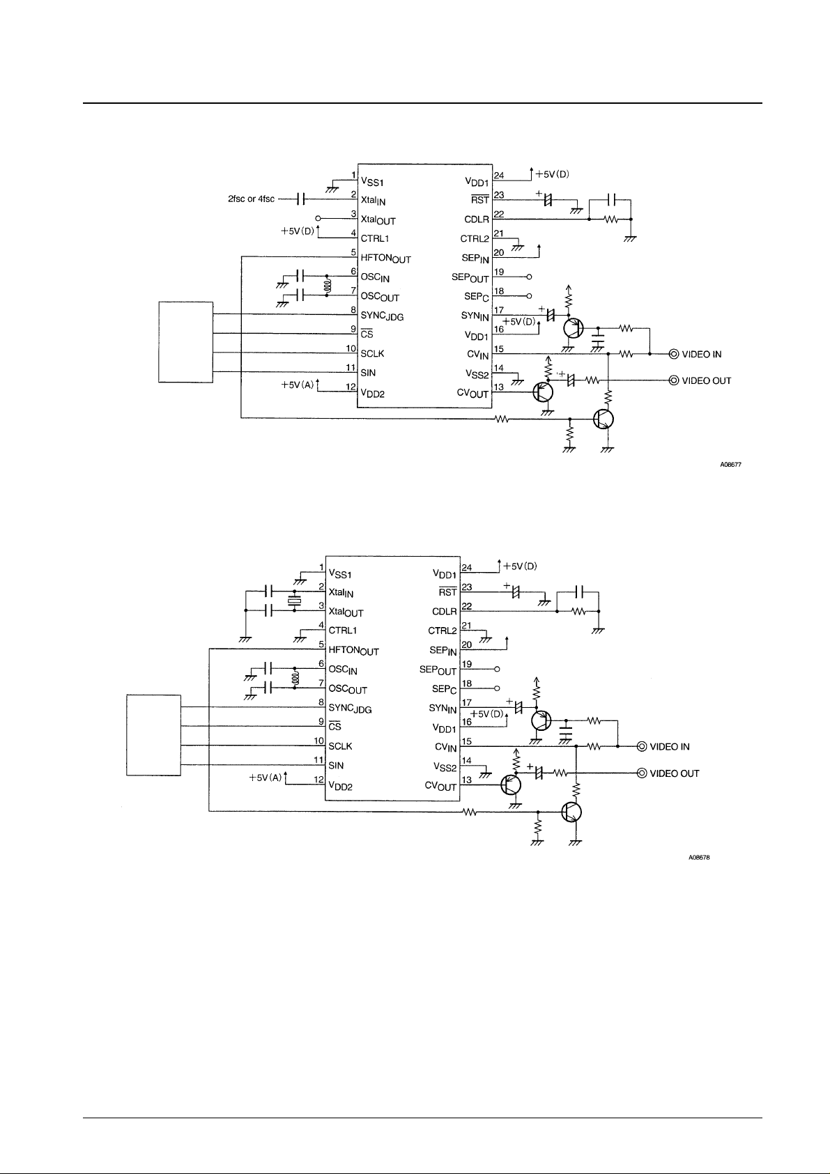
Sample Application Circuits (When the LC74786/M/JM is used in conjunction with a single-chip Y/C circuit.)
• Circuit Using an External System Clock Input
No. 5729-22/23
LC74786, 74786M, 74786JM
• Circuit Using a Crystal Oscillator
Micro-
controller
Micro-
controller

PS No. 5729-23/23
LC74786, LC74786M, LC74786JM
• Circuit Using an External System Clock Input (when the pin 3 and 4 functions are modified by mask options)
This catalog provides information as of March, 1998. Specifications and information herein are subject to
change without notice.
■ No products described or contained herein are intended for use in surgical implants, life-support systems, aerospace
equipment, nuclear power control systems, vehicles, disaster/crime-prevention equipment and the like, the failure of
which may directly or indirectly cause injury, death or property loss.
■ Anyone purchasing any products described or contained herein for an above-mentioned use shall:
➀ Accept full responsibility and indemnify and defend SANYO ELECTRIC CO., LTD., its affiliates, subsidiaries and
distributors and all their officers and employees, jointly and severally, against any and all claims and litigation and all
damages, cost and expenses associated with such use:
➁ Not impose any responsibility for any fault or negligence which may be cited in any such claim or litigation on
SANYO ELECTRIC CO., LTD., its affiliates, subsidiaries and distributors or any of their officers and employees
jointly or severally.
■ Information (including circuit diagrams and circuit parameters) herein is for example only; it is not guaranteed for
volume production. SANYO believes information herein is accurate and reliable, but no guarantees are made or implied
regarding its use or any infringements of intellectual property rights or other rights of third parties.
Note: When a sync tip level of 1.3 V DC (CVINinput signal: sync tip = 1.3 V) is selected for the internal generated video signals by option settings, the
electrolytic capacitor connected to SYN
IN
must be connected with the correct polarity.
Micro-
controller
 Loading...