

SANYO LC74785M, LC74785 Datasheet
Overview
The LC74785 and LC74785M are on-chip EDS CMOS
LSIs for on-screen display, a function that displays
characters and patterns on a TV screen under
microprocessor control. These LSIs support 12 × 18 dot
characters and can display 12 lines by 24 characters of
text.
Features
• Display format: 24 characters by 12 rows (Up to 288
characters)
• Character format: 12 (horizontal) × 18 (vertical) dots
• Character sizes: Three sizes each in the horizontal and
vertical directions
• Characters in font: 128
• Initial display positions: 64 horizontal positions and 64
vertical positions
• Blinking: Specifiable in character units
• Blinking types: Two periods supported: About 1.0
second and about 0.5 second
• Blanking: Over the whole font (12 × 18 dots)
• Background color
— Background coloring: 8 colors (internal synchronization
mode): 4fsc
— Background coloring: 6 colors (internal synchronization
mode): 2fsc
• Line background color
— Can be set for 3 lines
— Line background coloring: 8 colors (internal synchro-
nization mode): 4fsc
— Line background coloring: 6 colors (internal synchro-
nization mode): 2fsc
• External control input: 8-bit serial input format
• On-chip sync separator circuit
• EDS support
• Video output
— NTSC-format composite output
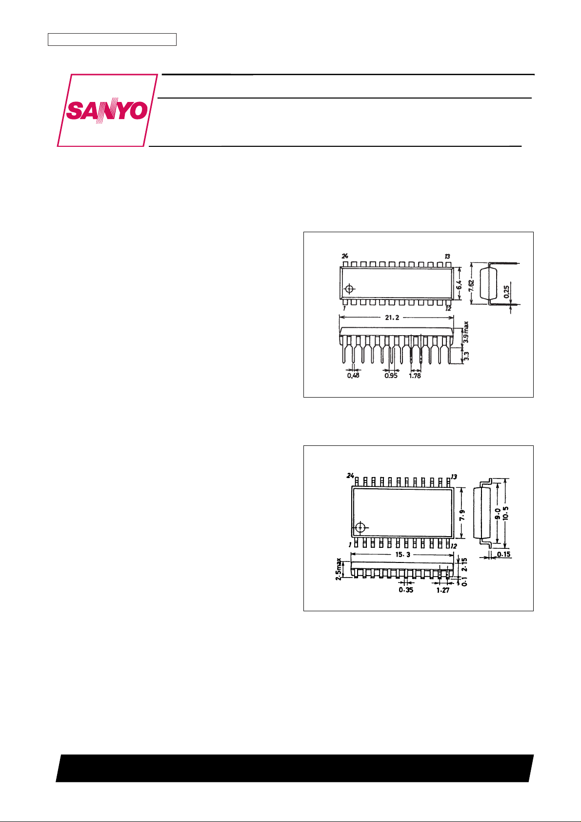
• Package
24-pin plastic DIP (300 mil)
24-pin plastic SOP (375 mil)
Package Dimensions
unit: mm
3067-DIP24S
unit: mm
3045B-MFP24
CMOS LSI
Ordering number : EN5520A
63097HA (OT) No. 5520-1/24
SANYO Electric Co.,Ltd. Semiconductor Bussiness Headquarters
TOKYO OFFICE Tokyo Bldg., 1-10, 1 Chome, Ueno, Taito-ku, TOKYO, 110 JAPAN
On-Screen Display Controller LSI
LC74785, LC74785M
SANYO: DIP24S
[LC74785]
SANYO: MFP24
[LC74785M]

Pin Assignment
Pin Functions
No. 5520-2/24
LC74785, LC74785M
Pin No. Pin Function Notes
1 V
SS
1 Ground Ground connection (digital system ground)
2 Xtal
IN
3
Xtal
OUT
(MUTE)
4
CTRL1
(CHABLK)
5 LN21 Data output
6 OSC
IN
LC oscillator
7 OSC
OUT
8 SYNC
JDG
Enable input pin for the OSD serial data input function.
9 CS1 Enable input Serial data input is enabled when this pin is low.
A pull-up resistor is built in. (The input has hysteresis characteristics.)
10 SCLK Clock input
Input for the serial data input clock.
A pull-up resistor is built in. (The input has hysteresis characteristics.)
11 SIN Data input
Serial data input. A pull-up resistor is built in. (The input has hysteresis
characteristics.)
12 V
DD
2 Power supply
Composite video signal level adjustment power supply (analog system power
supply)
13 CV
OUT
Video signal output Composite video signal output
14 V
SS
2 Ground Ground connection (analog system ground)
Crystal oscillator
(MUTE input)
Crystal oscillator input switching
(CHABLK output)
External synchronizing signal judgment output
These pins are used either to connect the crystal and capacitor used to form an
external crystal oscillator used to generate the internal synchronizing signals, or
to input an external clock signal (2fsc or 4fsc). As a mask option, the Xtalout pin
can be set to function as the MUTE input pin. When this pin is set low, the video
output is held at the pedestal level. (A pull-up resistor is built in and the input has
hysteresis characteristics.)
Switches the mode between external clock input and crystal oscillator operation.
A low level selects crystal oscillator operation and a high level selects external
clock input. As a mask option, the CTRL1 input pin can be set to function as the
CHABLK (character border) output. This is a 3-value output.
Connections for the coil and capacitor that form the character output dot clock
generation oscillator.
Line 21H pulse output
(Even fields when MOD1 is low, both fields when MOD1 is high)
Outputs the state of the external synchronizing signal presence/absence judgment. Outputs a
high level when synchronizing signals are present.
Outputs a field discrimination pulse (O/E pulse) when SEL2 is high.(HLFTON: Valid when 0)
HLFTON: A signal in the range specified by LNA*, LNB*, and LNC* is output when HLFTON is
high.)
Outputs the dot clock (LC oscillator) when CS1 is high and RST is low. (This signal is not
output on command resets.)
Outputs the crystal oscillator clock when CS1 is low and RST is low. (This signal is not output
on command resets.)
Continued on next page.
No. 5520-3/24
LC74785, LC74785M
Pin No. Pin Function Notes
15 CV
IN
Video signal input Composite video signal input
16 V
DD
1 Power supply Power supply (+5 V: digital system power supply)
17 SYN
IN
Sync separator circuit input Video signal input for the built-in sync separator circuit
18 CDLR Background color phase adjustment Background color phase adjustment. Connect to ground through a resistor and a capacitor.
19 SEP
OUT
Composite synchronizing signal output
20 SEP
IN
21 CS2 Enable input
22 CPDT Data output
23 RST Reset input
24 V
DD
1 Power supply (+5 V) Power supply (+5 V: digital system power supply)
Video signal output for the built-in sync separator circuit. Can be switched to function
as an output for signal (high or ST. pulse) due to MOD0 by setting SEL0 high.
Inputs the vertical synchronizing signal created by integrating the SEP
OUT
pin output
signal.
An integration circuit must be connected to the SEP
OUT
pin. This pin must be tied to
V
DD
1 if unused. This pin can be switched to function as the frame signal input mode
by setting SEL1 high. (This is valid when CTL3 is set to 1.)
Vertical synchronizing signal input
EDS data output enable input. EDS data output is enabled when this pin is low. A
pull-up resistor is built in. (The input has hysteresis characteristics.)
EDS data output (This pin can be either an n-channel open-drain output or a CMOS
output.)
System reset input
A pull-up resistor is built in. (The input has hysteresis characteristics.)
Continued from preceding page.
Note: Both VDD1 pins must be connected to the power supply.
Note: When the Xtal
IN
pin is used in clock input mode, extreme care must be taken to prevent noise from entering the input signal.
Parameter Symbol Conditions Ratings Unit
Supply voltage V
DD
VDD1 and VDD2 VSS–0.3 to VSS+7.0 V
Input voltage V
IN
All input pins VSS–0.3 to VDD+0.3 V
Output voltage V
OUT
LN21, CPDT, SEP
OUT
, and SYNC
JDG
VSS–0.3 to VDD+0.3 V
Allowable power dissipation Pd max Ta = 25°C 350 mW
Operating temperature Topr –30 to +70 °C
Storage temperature Tstg –40 to +125 °C
Specifications
Absolute Maximum Ratings at Ta = 25°C
Parameter Symbol Conditions
Ratings
Unit
min typ max
Supply voltage
V
DD
1 VDD1 4.5 5.0 5.5 V
V
DD
2 VDD2 4.5 5.0 1.27VDD1 V
V
IH
1
RST, CS1, CS2, SIN, SCLK, SEP
IN
,
0.8V
DD
1 VDD1 + 0.3 V
Input high-level voltage
and MUTE
V
IH
2 CTRL1 0.7VDD1 VDD1 + 0.3 V
V
IL
1
RST, CS1, CS2, SIN, SCLK, SEP
IN
,
V
SS
– 0.3 0.2VDD1 V
Input low-level voltage
and MUTE
V
IL
2 CTRL1 VSS– 0.3 0.3VDD1 V
Pull-up resistance R
PU
Applies to pins set for the RST, CS1, CS2,
25 50 90 kΩ
SIN, SCLK, and MUTE pin options.
Composite video signal input voltage
V
IN
1 CVIN; VDD1 = 5 V 2.0 Vp-p
V
IN
2 SYNIN; VDD1 = 5 V 1.5 2.0 2.5 Vp-p
Input voltage V
IN
3
Xtal
IN
(When external clock input is used)
0.10 5.0 Vp-p
f
in
= 2 fsc or 4 fsc ; VDD1 = 5 V
F
OSC
1
The Xtal
IN
and Xtal
OUT
oscillator pins
7.159 MHz
(2 fsc: NTSC)
Oscillator frequency
F
OSC
1
The Xtal
IN
and Xtal
OUT
oscillator pins
14.318 MHz
(4 fsc: NTSC)
F
OSC
2
The OSC
IN
and OSC
OUT
oscillator pins
5 10 MHz
(LC oscillator)
Allowable Operating Ranges at Ta = –30 to +70°C

No. 5520-4/24
LC74785, LC74785M
Parameter Symbol Conditions
Ratings
Unit
min typ max
Input off leakage current I
leak
1 CV
IN
1 µA
Output off leakage current I
leak
2 CV
OUT
1 µA
Output high-level voltage V
OH
1
LN21, SYNC
JDG
, CPDT, and SEP
OUT
;
3.5 V
V
DD
1 = 4.5 V, IOH= –1.0 mA
Output low-level voltage V
OL
1
LN21, SYNC
JDG
, CPDT, and SEP
OUT
;
1.0 V
V
DD
1 = 4.5 V, IOL= 1.0 mA
CHABLK; V
DD
1 = 5.0 V H 3.3 5.0 V
Three-value output voltage V
O
M 1.8 2.3 V
L 0 0.8 V
Input current
I
IH
RST, CS1, CS2, SIN, SCLK, CTRL1,
1 µA
SEP
IN
, and MUTE; VIN= VDD1
I
IL
CTRL1 and OSCIN; VIN= VSS1 –1 µA
Operating mode current drain
I
DD
1
V
DD
1; All outputs open, Xtal: 7.159 MHz,
30 mA
LC: 8 MHz
I
DD
2 VDD2: VDD2 = 5 V 20 mA
*
1
0.70 0.82 0.94 V
SYNC level V
SN
CV
OUT
; VDD1 = 5.0 V, VDD2 = 5.0 V *
2
0.89 1.01 1.13 V
*
3
1.18 1.30 1.42 V
*
1
1.32 1.44 1.56 V
Pedestal level V
PD
CV
OUT
; VDD1 = 5.0 V, VDD2 = 5.0 V *
2
1.52 1.64 1.76 V
*
3
1.81 1.93 2.05 V
*
1
0.98 1.10 1.22 V
Color burst low level V
CBL
CV
OUT
; VDD1 = 5.0 V, VDD2 = 5.0 V *
2
1.17 1.29 1.41 V
*
3
1.46 1.58 1.70 V
*
1
1.63 1.75 1.87 V
Color burst high level V
CBH
CV
OUT
; VDD1 = 5.0 V, VDD2 = 5.0 V *
2
1.83 1.95 2.07 V
*
3
2.11 2.23 2.35 V
*
1
1.17 1.29 1.41 V
Background color other than blue low level V
RSL
0 CV
OUT
; VDD1 = 5.0 V, VDD2 = 5.0 V *
2
1.36 1.48 1.60 V
*
3
1.65 1.77 1.89 V
*
1
2.33 2.45 2.57 V
Background color other than blue high level V
RSH
0 CV
OUT
; VDD1 = 5.0 V, VDD2 = 5.0 V *
2
2.52 2.64 2.76 V
*
3
2.81 2.93 3.05 V
*
1
1.08 1.20 1.32 V
Blue background color 1low level V
RSL
1 CV
OUT
; VDD1 = 5.0 V, VDD2 = 5.0 V *
2
1.27 1.39 1.51 V
*
3
1.56 1.68 1.80 V
*
1
1.49 1.61 1.83 V
Blue background color 2 low level V
RSL
2 CV
OUT
; VDD1 = 5.0 V, VDD2 = 5.0 V *
2
1.68 1.80 1.92 V
*
3
1.97 2.09 2.21 V
V
RSH
1
*
1
1.97 2.09 2.21 V
Blue background color 1, 2 high level CV
OUT
; VDD1 = 5.0 V, VDD2 = 5.0 V *
2
2.17 2.29 2.41 V
V
RSH
2
*
3
2.46 2.58 2.70 V
*
1
1.40 1.52 1.64 V
Frame level 0 V
BK
0 CV
OUT
; VDD1 = 5.0 V, VDD2 = 5.0 V *
2
1.60 1.72 1.84 V
*
3
1.89 2.01 2.13 V
*
1
1.97 2.09 2.21 V
Frame level 1 V
BK
1 CV
OUT
; VDD1 = 5.0 V, VDD2 = 5.0 V *
2
2.17 2.29 2.41 V
*
3
2.46 2.58 2.70 V
*
1
2.55 2.67 2.79 V
Character level V
CHA
CV
OUT
; VDD1 = 5.0 V, VDD2 = 5.0 V *
2
2.75 2.87 2.99 V
*
3
3.04 3.16 3.28 V
Electrical Characteristics at Ta = –30 to +70°C, VDD1 = 5 V unless otherwise specified.
Note: 1. When the sync level is 0.8 V
2. When the sync level is 1.0 V
3. When the sync level is 1.3 V
No. 5520-5/24
LC74785, LC74785M
Parameter Symbol Conditions
Ratings
Unit
min typ max
Minimum input pulse width
t
W(SCLK)
SCLK 200 ns
t
W(CS1)
CS1 (The period when CS1 is high) 1 µs
Data setup time
t
SU(CS1)
CS1 200 ns
t
SU(SIN)
SIN 200 ns
Data hold time
t
h(CS1)
CS1 2 µs
t
h(SIN)
SIN 200 ns
One word write time
t
word
The time to write 8 bits of data 4.2 µs
t
wt
The RAM data write time 1 µs
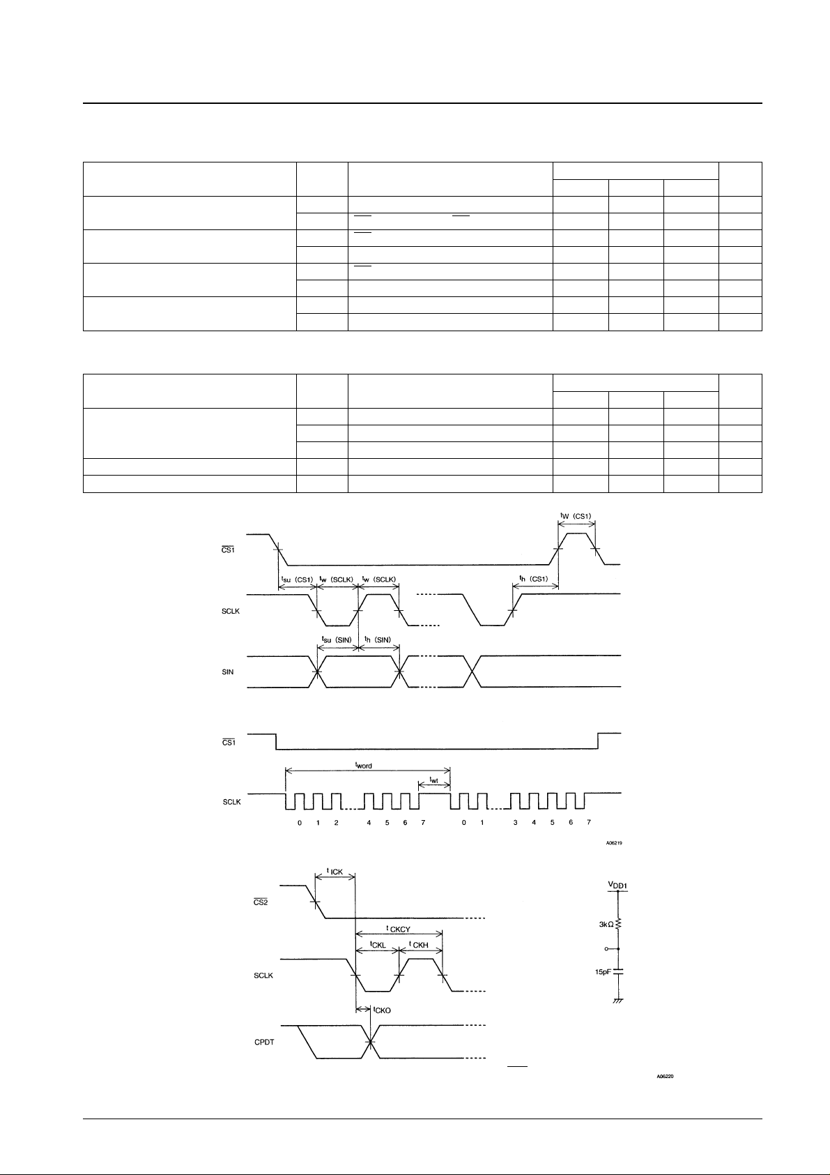
Timing Characteristics at Ta = –30 to +70°C, VDD1 = 5 ±0.5 V
OSD write (See Figure 1.)
Parameter Symbol Conditions
Ratings
Unit
min typ max
t
CKCY
SCLK 2 µs
Minimum input pulse width t
CKL
SCLK 1 µs
t
CKH
SCLK 1 µs
Setup time t
ICK
SCLK 10 µs
Output delay time t
CKO
CPDT 0.5 µs
EDS read (For the n-channel open-drain circuit, see Figure 2.)
Figure 1 OSD Serial Data Input Timing
Figure 2 EDS Serial Output Test Conditions (For the n-channel open-drain circuit.)
Note: The CMOS output circuit follows the OSD timing.
First byte
Note: CPDT goes to the high-impedance state when CS2 is high.
Second byte
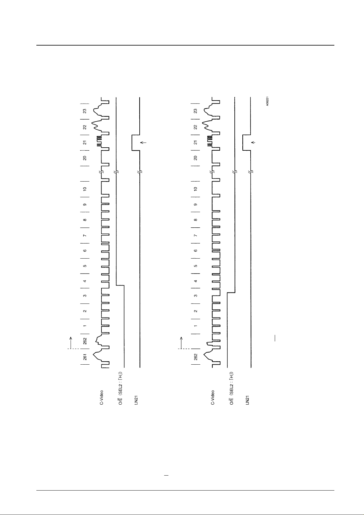
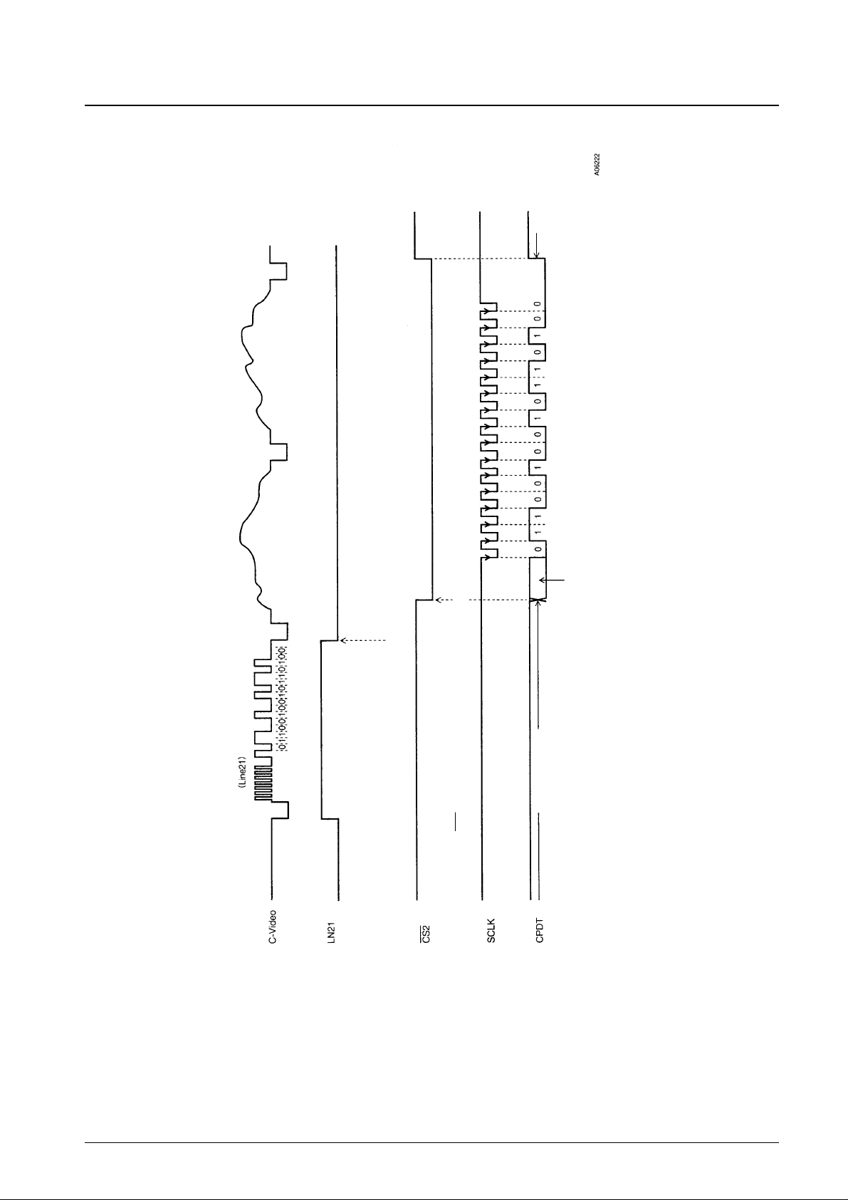
Figure 3 O/E and LN21 Output Timing
No. 5520-6/24
LC74785, LC74785M
Note: The O/E signal is output from the SYNC
JDG
pin when SEL2 is high.
LN21 is output for even fields when MOD1 is low and for both fields when MOD1 is high.
(Line number)
Odd field
Pulse output when MOD1 is high
Pulse output when MOD1 is low or high
Even field
(Line number)
No. 5520-7/24
LC74785, LC74785M
Figure 4 Transferring caption data from the LC74785/M to the decoder LSI (microcontroller): Method 1
(Basic LC74785/M usage)
Note: When extracting closed caption character data when MOD1 is high (NTSC-TV), applications must determine whether the current field is odd or
even by checking the signal level output from the SYNC
JDG
pin (with SEL2 set high) when a falling edge is detected on LN21.
A pulse is output at line 21 in even fields when MOD1 is low.
A pulse is output at line 21 in both fields when MOD1 is High.
Caption data is transferred to the data output buffer.
High-impedance
High-impedance
The previous data is output.
The 16 bits of caption data is output LSB first
in synchronization with SCLK falling edges.
CS2 is switched from high to low after the decoder LSI (microcontroller) detects a falling edge on LN21.

No. 5520-8/24
LC74785, LC74785M
The timing of the transfer of caption data to the data output buffer is synchronized with the falling edge of the pulse
output from LN21. Therefore, the software processing shown below is required if the decoder LSI (microcontroller) does
not detect LN21 falling edges.
Since data is output to the output buffer once (during the even field) when MOD1 is low, the data transfer control
operation from the decoder LSI (microcontroller) must be performed at least twice in a single frame (about 32 ms).
If a transfer control operation is performed twice in the same frame, the CPDT output on the second operation will be 16
bits of zero data. This allows the decoder LSI to determine that the data for the next frame has not been transferred yet.
Note: If CS2 remains low, the hardware will not be able to transfer the data to the output buffer. Therefore, the decoder LSI (microcontroller) must reset CS2
to high from low after it completes a data transfer control operation.
Transfer method 2 cannot be used if MOD1 is high (NTSC-TV).
Transfer of 16 data bits
Activity within a given frame (MOD1: low)
Data in which all
16 bits are zero
Figure 5 Transferring caption data from the LC74785/M to the decoder LSI (microcontroller): Method 2
(When it is not possible to allocate a port on the decoder LSI (microcontroller) to detect
falling edges on LN21.)
 Loading...