

Page 1
CMOS LSI
Ordering number : EN4989A
92595HA/63095TH (OT) No. 4989-1/16
SANYO Electric Co.,Ltd. Semiconductor Bussiness Headquarters
TOKYO OFFICE Tokyo Bldg., 1-10, 1 Chome, Ueno, Taito-ku, TOKYO, 110-8534 JAPAN
On-Screen Display Controller LSI
for VCR Products
LC74782, 74782M
Overview
The LC74782 and LC74782M are on-screen display
CMOS LSIs that display characters and patterns on a TV
screen under microprocessor control. The LC74782 and
LC74782M display up to 12 lines of 24 characters, each in
a 12 × 18 dot matrix.
Features
• Display structure: 12 lines × 24 characters (up to
288 characters)
• Character structure: 12 (horizontal) × 18 (vertical) dots
• Character sizes: Three size settings each in the vertical
and horizontal directions
• Character set: 256 characters
• Display start position: 64 position settings each in the
vertical and horizontal directions
• Blinking: In individual character units
• Blinking types: Two types with periods of about 0.5 and
1.0 second
• Blanking: Whole font area blanking (12 × 18 dots)
• Background colors: 8 colors (in internal synchronization
mode): 4fSC (NTSC/PAL/PAL-M/
PAL-N)
Background colors: 4 colors (in internal synchronization
mode): 2fSC (NTSC)
Background colors: 1 color (blue) (in internal
synchronization mode): 2fSC
(PAL/PAL-M/PAL-N)
• External control input: 8-bit serial input format
• Built-in sync separator circuit
• Character blanked data output
• Video output: Compound NTSC, PAL, PAL-N and
PAL-M output
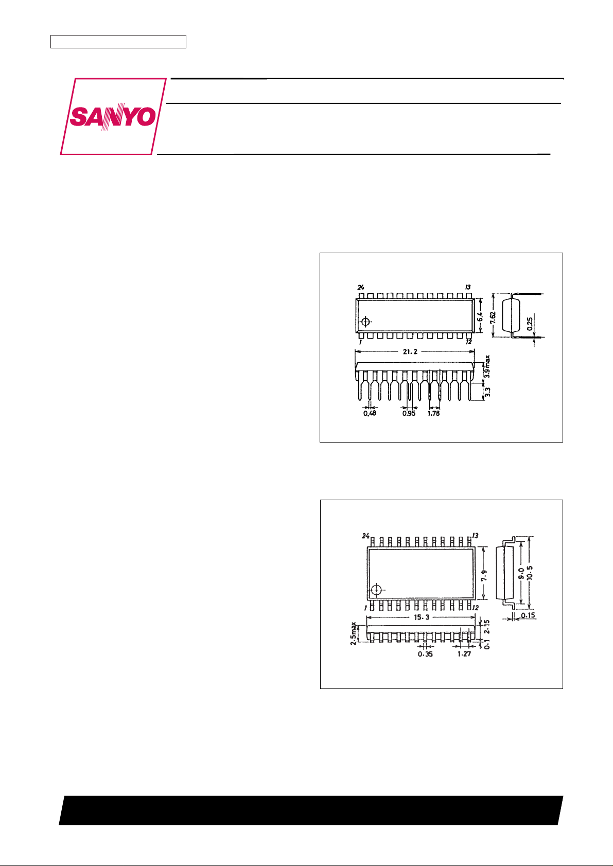
Package Dimensions
unit: mm
3067-DIP24S
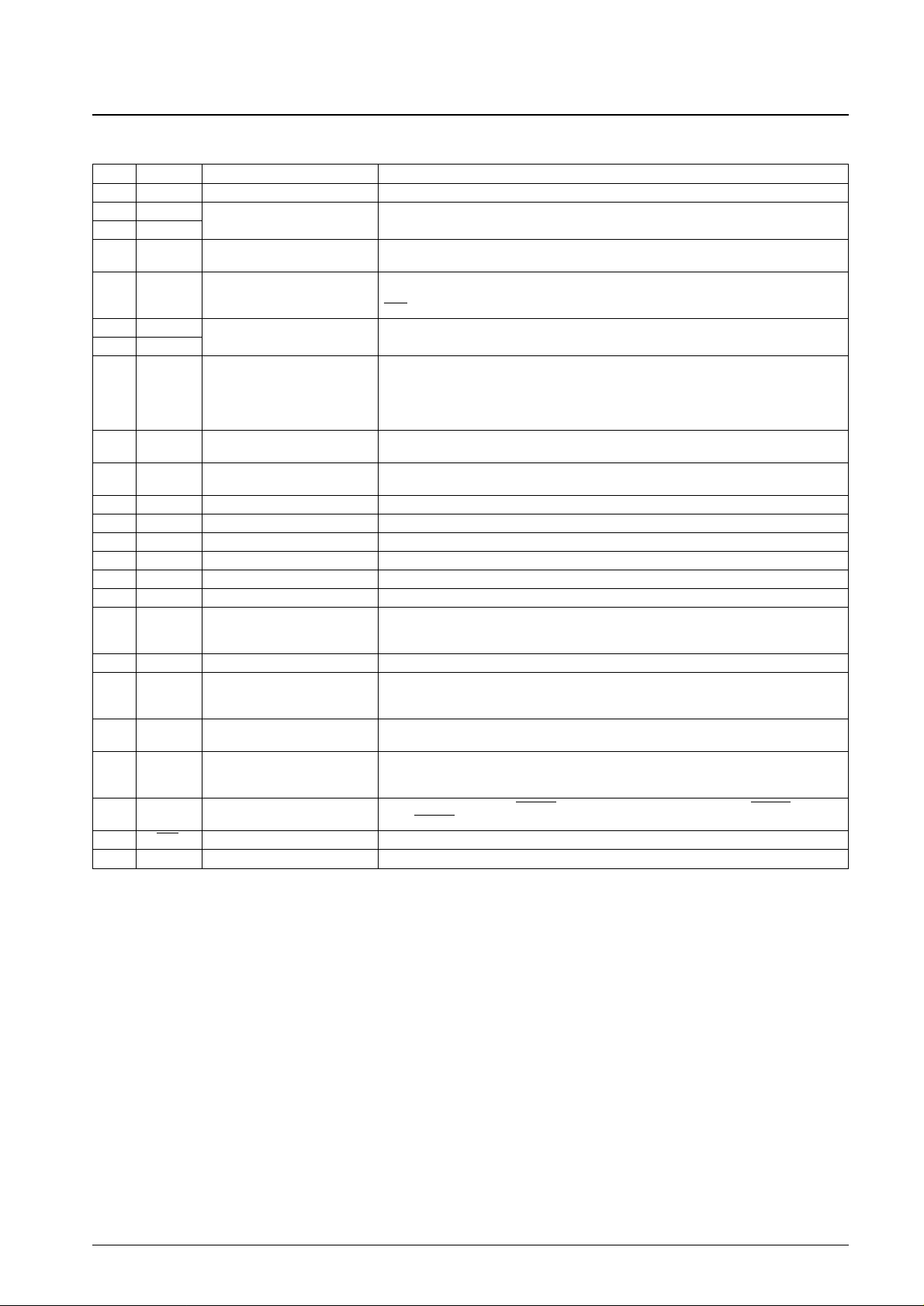
unit: mm
3045B-MFP24
SANYO: MFP24
[LC74782M]
[LC74782]
SANYO: DIP24S
Page 2
Pin Functions
No. 4989-2/16
LC74782, 74782M
Pin No. Symbol Function Description
1 V
SS
1 Ground Ground connection (digital system ground)
2 Xtal
IN
Crystal oscillator connection
Used to connect the crystal oscillator and capacitor used to generate the internal
3 Xtal
OUT
synchronization signal, or to input an external clock (2fsc or 4fsc).
4 CTRL1 Crystal oscillator input switching
Switches between external clock input mode and crystal oscillator mode.
Low = crystal oscillator mode, high = external clock mode
Outputs the blank signal (the OR of the character and border signals). (Outputs a composite
5 BLANK Blanking output sync signal when MOD0 is high.) Outputs the crystal oscillator clock during reset (when the
RST pin is low), but can be set up to not output this signal by microprocessor command.
6 OSC
IN
LC oscillator connection
Connections for the coil and capacitor that form the oscillator that generates the character
7 OSC
OUT
output dot clock.
Outputs the character signal. (Functions as the external synchronization signal discrimination
signal output pin when MOD0 is high, and outputs the state of the judgment as to whether the
8 CHARA Character output external synchronization signal is present or not. Outputs a high level when the synchronization
signal is present.) Outputs the dot clock (LC oscillator) during reset, but can be set up to not
output this signal by microprocessor command.
9 CS Enable input
Serial data input enable input. Serial data input is enabled when low. A pull-up resistor is built in
(hysteresis input).
10 SCLK Clock input
Serial data input clock input.
A pull-up resistor is built in (hysteresis input).
11 SIN Data input Serial data input. A pull-up resistor is built in (hysteresis input).
12 V
DD
2 Power supply Composite video signal level adjustment power supply pin (analog system power supply).
13 CV
OUT
Video signal output Composite video signal output
14 NC Must be either connected to ground or left open.
15 CV
IN
Video signal input Composite video signal input
16 V
DD
1 Power supply Power supply (+5 V: digital system power supply)
Video signal input for the built-in sync separator circuit (Used for either horizontal
17 SYN
IN
Sync separator circuit input synchronization signal or composite sync signal input when the built-in sync separator circuit is
not used.)
18 SEP
C
Sync separator circuit bias voltage Built-in sync separator circuit bias voltage monitor pin
Built-in sync separator circuit composite sync signal output. (When MOD1 is high, outputs a high
19 SEP
OUT
Composite sync signal output level during internal synchronization and a low level during external synchronization.) (Outputs
the SYN
IN
input signal when the internal sync separator circuit is not used.)
20 SEP
IN
Vertical synchronization Inputs a vertical synchronization signal created by integrating the SEP
OUT
pin output signal. An
signal input integrator must be attached at the SEP
OUT
pin. This pin must be tied to VDD1 if unused.
The setting indicated by this pin takes priority in switching between the NTSC, PAL, PAL-M and
21 CTRL2 NTSC/PAL-M switching input PAL-N formats. A low level selects NTSC after a reset. The microprocessor command NTSC,
PAL, PAL-M, or PAL-N setting is valid. High = PAL-M format.
22 CTRL3 SEP
IN
input control
Controls whether or not the VSYNC signal is input to the SEP
IN
input. Low = VSYNC input,
high = VSYNC not input.
23 RST Reset input System reset input. A pull-up resistor is built in (hysteresis input).
24 V
DD
1 Power supply (+5 V) Power supply (+5 V: digital system power supply)
Page 3

Pin Assignment
Specifications
Absolute Maximum Ratings at Ta = 25°C
Allowable Operating Ranges at Ta = –30 to +70°C
Note: If the XtalINpin is used in clock input mode, be sure to prevent input noise from becoming a problem.
No. 4989-3/16
LC74782, 74782M
Parameter Symbol Conditions Ratings Unit
Maximum supply voltage V
DD
max VDD1 and VDD2 pins VSS– 0.3 to VSS+ 7.0 V
Maximum input voltage V
IN
max All pins VSS– 0.3 to VDD+ 0.3 V
Maximum output voltage V
OUT
max BLANK, CHARA and SEP
OUT
pins VSS– 0.3 to VDD+ 0.3 V
Allowable power dissipation Pd max Ta = 25°C 350 mW
Operating temperature Topr –30 to +70 °C
Storage temperature Tstg –40 to +125 °C
Parameter Symbol Conditions min typ max Unit
Supply voltage
V
DD
1 VDD1 pin 4.5 5.0 5.5 V
V
DD
2 VDD2 pin 4.5 5.0 1.27 VDD1 V
Input high level voltage
V
IH
1 RST, CS, SIN and SCLK pins 0.8 VDD1 VDD1 + 0.3 V
V
IH
2 CTRL1, CTRL2, CTRL3 and SEPINpins 0.7 VDD1 VDD1 + 0.3 V
Input low level voltage
V
IL
1 RST, CS, SIN and SCLK pins VSS– 0.3 0.2 VDD1 V
V
IL
2 CTRL1, CTRL2, CTRL3 and SEPINpins VSS– 0.3 0.3 VDD1 V
Pull-up resistance R
PU
RST, CS, SIN and SCLK pins, applies to pins set
25 50 90 kΩ
by options.
Composite video input voltage
V
IN
1 CVINpin: VDD1 = 5 V 2.0 Vp-p
V
IN
2 SYNINpin: VDD1 = 5 V 2.0 2.5 Vp-p
Input voltage V
IN
3
Xtal
IN
pin (in external clock input mode),
0.10 5.0 Vp-p
f
in
= 2fsc or 4fsc: VDD1 = 5 V
F
OSC
1 XtalINand Xtal
OUT
oscillator pins (2fsc: NTSC) 7.159 MHz
F
OSC
1 XtalINand Xtal
OUT
oscillator pins (4fsc: NTSC) 14.318 MHz
F
OSC
1 XtalINand Xtal
OUT
oscillator pins (2fsc: PAL) 8.867 MHz
F
OSC
1 XtalINand Xtal
OUT
oscillator pins (4fsc: PAL) 17.734 MHz
Oscillator frequency F
OSC
1 XtalINand Xtal
OUT
oscillator pins (2fsc: PAL-M) 7.151 MHz
F
OSC
1 XtalINand Xtal
OUT
oscillator pins (4fsc: PAL-M) 14.302 MHz
F
OSC
1 XtalINand Xtal
OUT
oscillator pins (2fsc: PAL-N) 7.164 MHz
F
OSC
1 XtalINand Xtal
OUT
oscillator pins (4fsc: PAL-N) 14.328 MHz
F
OSC
2 OSCINand OSC
OUT
oscillator pins (LC oscillator) 5 10 MHz
Page 4
Electrical Characteristics at Ta = –30 to +70°C, VDD1 = 5 V unless otherwise specified
Note: 1. When the sync level is 0.8 V.
2. When the sync level is 1.0 V.
Timing Characteristics at Ta = –30 to +70°C, VDD1 = 5 ± 0.5 V
No. 4989-4/16
LC74782, 74782M
Parameter Symbol Conditions min typ max Unit
Input off leakage current I
leak
1 CVINpin 1 µA
Output off leakage current I
leak
2 CV
OUT
pin 1 µA
Output high level voltage V
OH
1
BLANK, CHARA and SEP
OUT
pins: VDD1 = 4.5 V,
3.5 V
I
OH
= –1.0 mA
Output low level voltage V
OL
1
BLANK, CHARA and SEP
OUT
pins: VDD1 = 4.5 V,
1.0 V
I
OH
= 1.0 mA
Input current
I
IH
RST, CS, SIN, SCLK, CTRL1, CTRL3 and SEPINpins:
1 µA
V
IN
= VDD1
I
IL
CTRL1, CTRL2, CTRL3 and OSCINpins: VIN= VSS1 –1 µA
Operating current drain
I
DD
1
V
DD
1 pin; all outputs: open, Xtal: 7.159 MHz,
15 mA
LC: 8 MHz
I
DD
2 VDD2 pin: VDD2 = 5 V 20 mA
Sync level V
SN
CV
OUT
pin
V
DD
1 = 5.0 V,
*1 0.70 0.82 0.94 V
V
DD
2 = 5.0 V
*2 0.91 1.03 1.15 V
Pedestal level V
PD
CV
OUT
pin
V
DD
1 = 5.0 V,
*1 1.31 1.43 1.55 V
V
DD
2 = 5.0 V
*2 1.53 1.65 1.77 V
Color burst low level V
CBL
CV
OUT
pin
V
DD
1 = 5.0 V,
*1 1.00 1.12 1.24 V
V
DD
2 = 5.0 V
*2 1.21 1.33 1.45 V
Color burst high level V
CBH
CV
OUT
pin
V
DD
1 = 5.0 V,
*1 1.63 1.75 1.87 V
V
DD
2 = 5.0 V
*2 1.84 1.96 2.08 V
Background color low level V
RSL
CV
OUT
pin
V
DD
1 = 5.0 V,
*1 1.47 1.59 1.71 V
V
DD
2 = 5.0 V
*2 1.68 1.80 1.92 V
Background color high level V
RSH
CV
OUT
pin
V
DD
1 = 5.0 V,
*1 1.99 2.11 2.23 V
V
DD
2 = 5.0 V
*2 2.19 2.31 2.43 V
Border level 0 V
BK
0 CV
OUT
pin
V
DD
1 = 5.0 V,
*1 1.42 1.54 1.66 V
V
DD
2 = 5.0 V
*2 1.63 1.75 1.87 V
Border level 1 V
BK
1 CV
OUT
pin
V
DD
1 = 5.0 V,
*1 1.99 2.11 2.23 V
V
DD
2 = 5.0 V
*2 2.19 2.31 2.43 V
Character level V
CHA
CV
OUT
pin
V
DD
1 = 5.0 V,
*1 2.58 2.70 2.82 V
V
DD
2 = 5.0 V
*2 2.78 2.90 3.02 V
Parameter Symbol Conditions min typ max Unit
Minimum input pulse width
t
W (SCLK)
SCLK pin 200 ns
t
W (CS)
CS pin (the period when CS is high) 1 µs
Data setup time
t
SU (CS)
CS pin 200 ns
t
SU (SIN)
SIN pin 200 ns
Data hold time
t
h (CS)
CS pin 2 µs
t
h (SIN)
SIN pin 200 ns
One word write time
t
word
8-bit data write time 4.2 µs
t
wt
RAM data write time 1 µs
Page 5
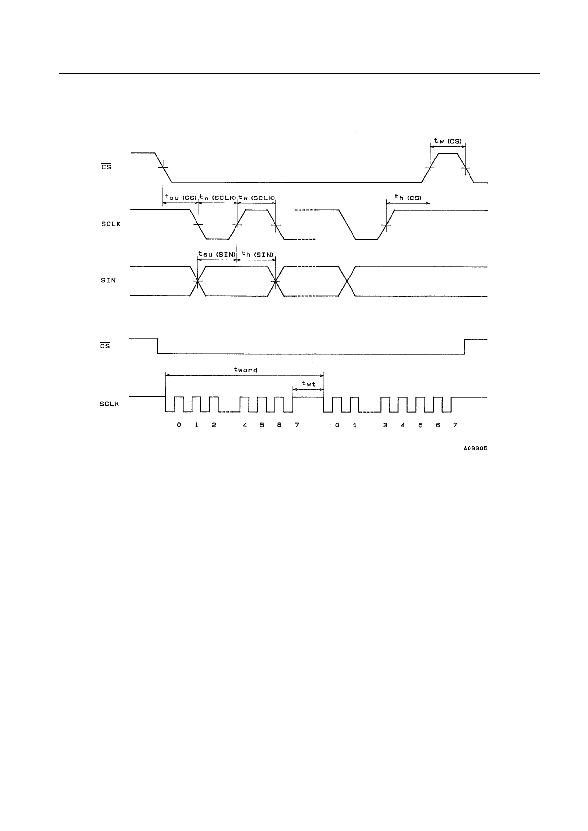
Serial Data Input Timing
No. 4989-5/16
LC74782, 74782M
Page 6

System Block Diagram
No. 4989-6/16
LC74782, 74782M
Page 7

Display Control Commands
The display control commands have a serial input format with 8-bit units. A command consists of a command identifier
code in the first byte and data in the second and subsequent bytes. There are eight commands as listed below.
① COMMAND0: Display memory (VRAM) write address setup command
② COMMAND1: Display character data write command
③ COMMAND2: Vertical display start position and vertical character size setup command
④ COMMAND3: Horizontal display start position and horizontal character size setup command
⑤ COMMAND4: Display control setup command
⑥ COMMAND5: Display control setup command
⑦ COMMAND6: Synchronization signal detection setup command
⑧ COMMAND7: Display control setup command
Display Control Command Table
Once written, the command identifier code in the first byte is stored until the next first byte is written. However, when
the display character data write command (COMMAND1) is written, the LC74782/M locks into the display character
data write mode, and another first byte cannot be written.
When a high level is input to the CS pin, the LC74782/M is set to COMMAND0 (display memory write address setup
mode).
No. 4989-7/16
LC74782, 74782M
First byte Second byte
Command
Command identification code
Data Data
7 6 5 4 3 2 1 0 7 6 5 4 3 2 1 0
COMMAND0 1 0 0 0 V3 V2 V1 V0 0 0 0 H4 H3 H2 H1 H0
(Set write address)
COMMAND1 1 0 0 1 0 0 0 at c7 c6 c5 c4 c3 c2 c1 c0
(Write character)
COMMAND2
1 0 1 0 VS VS VS VS 0 FS VP VP VP VP VP VP
(Set vertical display start position and
21 20 11 10 5 4 3 2 1 0
vertical character size)
COMMAND3
1 0 1 1 HS HS HS HS 0 LC HP HP HP HP HP HP
(Set horizontal display start position
21 20 11 10 5 4 3 2 1 0
and horizontal character size)
COMMAND4 1 1 0 0 TST RAM OSC SYS 0 BLK BLK BLK BK BK RV DSP
(Display control) MOD ERS STP RST 2 1 0 1 0 ON
COMMAND5 1 1 0 1 NP NP NON INT 0 0 0 BCL CB PH PH PH
(Display control) 1 0 2 1 0
COMMAND6 1 1 1 0 MOD MOD DIS MUT 0 RN RN RN SN SN SN SN
(Synchronization signal detection) 1 0 LIN 2 1 0 3 2 1 0
COMMAND7 1 1 1 1 EX PD EX PD 0 0 0 VNP VSP MSK MSK EGL
(Display control) 1 1 0 0 SEL SEL ERS SEL
Page 8

① COMMAND0 (Display memory write address setup command)
First byte
Second byte
Note: The register states are all set to zero when the LC74782/M is reset with the RST pin.
② COMMAND1 (Display character data write setup command)
First byte
No. 4989-8/16
LC74782, 74782M
Register content
DA0 to DA7 Register name
State Function
Note
7 — 1
6 — 0
Command 0 identification code
5 — 0 Set the display memory write address.
4 — 0
3 V3
0
1
2 V2
0
1
Display memory address (0 to B hexadecimal)
1 V1
0
1
0 V0
0
1
Register content
DA0 to DA7 Register name
State Function
Note
7 — 0 Second byte identification bit
6 — 0
5 — 0
4 H4
0
1
3 H3
0
1
2 H2
0
Display memory address (0 to 17 hexadecimal)
1
1 H1
0
1
0 H0
0
1
Register content
DA0 to DA7 Register name
State Function
Note
7 — 1
6 — 0
Command 1 identification code
5 — 0
Set up display character data write.
4 — 1
3 — 0
2 — 0
1 — 0
0 at
0 Character attribute off
1 Character attribute on
When this command is input, the
LC74782/M locks into the display
character data write mode until the CS
pin goes high.
Page 9
Second byte
Note: The register states are all set to zero when the LC74782/M is reset with the RST pin.
③ COMMAND2 (Vertical display start position and vertical character size setup command)
First byte
No. 4989-9/16
LC74782, 74782M
Register content
DA0 to DA7 Register name
State Function
Note
7 c7
1
0
6 c6
0
1
5 c5
0
1
4 c4
0
1
3 c3
0
Character code (00 to FF hexadecimal)
1
2 c2
0
1
1 c1
0
1
0 c0
0
1
Register content
DA0 to DA7 Register name
State Function
Note
7 — 1
6 — 0
Command 2 identification code
5 — 1 Set the vertical display start position and vertical character size.
4 — 0
3 VS21
0
1
Second line vertical character size
2 VS20
0
1
1 VS11
0
1
First line vertical character size
0 VS10
0
1
VS21
VS20
0 1
0 1H per dot 2H per dot
1 3H per dot 1H per dot
VS11
VS10
0 1
0 1H per dot 2H per dot
1 3H per dot 1H per dot
Page 10

Second byte
Note: The register states are all set to zero when the LC74782/M is reset with the RST pin.
④ COMMAND3 (Horizontal display start position and horizontal character size setup command)
First byte
Second byte
Note: The register states are all set to zero when the LC74782/M is reset with the RST pin.
No. 4989-10/16
LC74782, 74782M
Register content
DA0 to DA7 Register name
State Function
Note
7 — 1
6 — 0
Command 3 identification code
5 — 1
Set the horizontal display start position and horizontal
4 — 1
character size.
3 HS21
0
1
Second line horizontal character size
2 HS20
0
1
1 HS11
0
1
First line horizontal character size
0 HS10
0
1
HS21
HS20
0 1
0 1 Tc per dot 2 Tc per dot
1 3 Tc per dot 1 Tc per dot
HS11
HS10
0 1
0 1 Tc per dot 2 Tc per dot
1 3 Tc per dot 1 Tc per dot
Register content
DA0 to DA7 Register name
State Function
Note
7 — 0 Second byte identification bit
6 LC
0 An LC oscillator is used for the dot clock.
Selects the dot clock used in horizontal
1 A crystal oscillator is used for the dot clock.
character display.
5
HP5
0 If HS is the horizontal start position then:
(MSB)
1
5
4 HP4
0
HS = Tc × (2Σ 2
n
HPn)
1
n = 0
3 HP3
0
1
2 HP2
0
1
1 HP1
0
1
0
HP0
0
(LSB)
1
The horizontal display start position is
set by the six bits HP5 to HP0.
The weight of bit 1 is 2Tc.
Tc: Period of the oscillator connected to OSCIN/OSCOUT in
operating mode.
Register content
DA0 to DA7 Register name
State Function
Note
7 — 0 Second byte identification bit
6 FS
0 Crystal oscillator frequency: 2fsc
1 Crystal oscillator frequency: 4fsc
5
VP5
0
(MSB)
1
4 VP4
0
1
3 VP3
0
1
2 VP2
0
1
1 VP1
0
1
0
VP0
0
(LSB)
1
The vertical display start position is set
by the 6 bits VP0 to VP5.
The weight of bit 1 is 2H.
If VS is the vertical display start position then:
5
VS = H × (2Σ 2nVPn)
n = 0
H: the horizontal synchronization pulse period
Page 11
⑤ COMMAND4 (Display control setup command)
First byte
Second byte
Note: The register states are all set to zero when the LC74782/M is reset with the RST pin.
No. 4989-11/16
LC74782, 74782M
Register content
DA0 to DA7 Register name
State Function
Note
7 — 0 Second byte identification bit
6 BLK2
0 Character display block
Full character size specification
1 Video display block
5
BLK1
0
1
Changes the blanking size.
4 BLK0
0
1
3 BK1
0 Blinking period: about 0.5 s
Switches the blinking period.
1 Blinking period: about 1.0 s
0 Blinking off
When blinking is specified for reversed
2 BK0
characters, the blinking will be between
1 Blinking on
normal character and reversed character
display.
1 RV
0 Reverse (character reversing) off
1 Reverse (character reversing) on
0
DSPON
0 Character display off
1 Character display on
BLK1
BLK0
0 1
0 Blanking off Character size
1 Border size Full character size
Register content
DA0 to DA7 Register name
State Function
Note
7 — 1
6 — 1
Command 4 identification code
5 — 0 Display control
4 — 0
3 TSTMOD
0 Normal operating mode
This bit must be zero.
1 Test mode
0
The RAM erase operation requires about
2 RAMERS 500 µs (It is executed in the DSPOFF
1 Erase display RAM (set to FF hexadecimal)
state.)
1 OSCSTP
0 Do not stop the crystal oscillator and LC oscillator circuits.
Valid when character display is off in
1 Stop the crystal oscillator and LC oscillator circuits.
external synchronization mode.
0 SYSRST
0
Reset occurs when the CS pin is low, and
1 Reset all registers and turn the display off.
the reset is cleared when CS goes high.
Page 12

⑥ COMMAND5 (Display control setup command)
First byte
Second byte
Note: The register states are all set to zero when the LC74782/M is reset with the RST pin.
No. 4989-12/16
LC74782, 74782M
Register content
DA0 to DA7 Register name
State Function
Note
7 — 0 Second byte identification bit
6 — 0
5 — 0
4 BCL
0 Background color present
Only valid with internal synchronization.
1 No background color (only the background level is set)
3 CB
0 Outputs a color burst signal.
Only valid when BCL is high.
1 Stops color burst signal output.
0
2 PH2
1
0
1 PH1
1
0
0 PH0
1
Sample background color phase
diagram for PAL mode color burst
*: When 2fsc NTSC is used
Phase 2 Phase 1 Phase 0
Background color (phase)
NTSC PAL
0 0 0 π/2* ±π/2
0 0 1 In phase* In phase
0 1 0 3π/2* π/2
0 1 1 π* ±π
1 0 0 3π/4 ±3π/4
1 0 1 π/4 ±π/4
1 1 0 7π/4 π/4
1 1 1 5π/4 3π/4
–
+
–
+
–
+
Register content
DA0 to DA7 Register name
State Function
Note
7 — 1
6 — 1
Command 5 identification code
5 — 0
Display control
4 — 1
3 NP1
0
1
Switches between NTSC, PAL, PAL-M
2 NP0
0
and PAL-N
1
1 NON
0 Interlaced
Switches between interlaced and non-
1 Non-interlaced
interlaced displays
0 INT
0 External synchronization
Switches between external and internal
1 Internal synchronization
synchronization
NP1
NP0
0 1
0 NTSC PAL-M
1 PAL PAL-N
Page 13

⑦ COMMAND6 (Synchronization signal detection setup command)
First byte
Second byte
Note: The register states are all set to zero when the LC74782/M is reset with the RST pin.
⑧ COMMAND7 (Display control setup command)
First byte
No. 4989-13/16
LC74782, 74782M
Register content
DA0 to DA7 Register name
State Function
Note
7 — 0 Second byte identification bit
6 RN2
0
1
5
RN1
0
1
4 RN0
0
1
3 SN3
0
1
2 SN2
0
1
1 SN1
0
1
0
SN0
0
1
External synchronization signal
detection control
Signal present to absent transition
recognition
Setting for the sampling period when
SYNC can not be detected
consecutively in the horizontal
synchronization signal period (1H).
External synchronization signal detection
control
Signal absent to present transition
recognition
Setting for the sampling period when
SYNC can be detected consecutively in
the horizontal synchronization signal
period (1H).
RN2 RN1 RN0 Number of times HSYNC detected
0 0 0 0 times
0 0 1 4 times
0 1 0 8 times
1 0 0 16 times
SN3 SN2 SN1 SN0 Number of times HSYNC detected
0 0 0 0 Not detected
0 0 0 1 32 times
0 0 1 0 64 times
0 1 0 0 128 times
1 0 0 0 256 times
Register content
DA0 to DA7 Register name
State Function
Note
7 — 1
6 — 1
Command 7 identification code
5 — 1 Display control setup
4 — 1
3 EX1
0 MODE1 setting output
Switches the SEP
OUT
(pin 19) output
1 PORT DATA1 setting output
2 PD1
0 The output is set low.
1 The output is set high.
1 EX0
0 MODE0 setting output
Switches the BLANK (pin 5) output
1 PORT DATA0 setting output
0 PD0
0 The output is set low.
1 The output is set high.
Register content
DA0 to DA7 Register name
State Function
Note
7 — 1
6 — 1
Command 6 identification code
5 — 1
Synchronization signal control settings
4 — 0
3 MOD1
0 Sync separator circuit signal
Switches the SEP
OUT
(pin 19) output
1 High level output during internal synchronization
0
Pin 5: Blank signal
2 MOD0
Pin 8: Character signal
Switches the BLANK (pin 5) and CHARA
1
Pin 5: Composite synchronization signal
(pin 8) outputs
Pin 8: External synchronization signal discrimination output signal
1 DISLIN
0 12 lines
Switches the number of display lines.
1 10 lines
0 MUT
0 Normal output
Switches CV
OUT
1 CVINis cut and CV
OUT
is fixed at the pedestal level.
Page 14
Second byte
Note: The register states are all set to zero when the LC74782/M is reset with the RST pin.
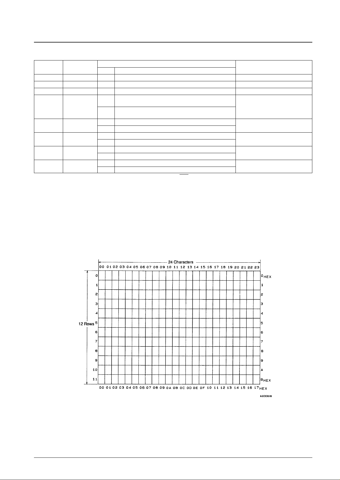
Display Screen Structure
The display consists of 24 characters × 12 rows.
The maximum number of displayed character is 288.
The maximum number of characters is reduced to less than 288 when the character size is enlarged.
Display memory addresses are specified as row (0 to 11 decimal) and column (0 to 23 decimal) addresses.
Display Screen Structure (display memory addresses)
No. 4989-14/16
LC74782, 74782M
Register content
DA0 to DA7 Register name
State Function
Note
7 — 0 Second byte identification bit
6 — 0
5 — 0
0
V falling edge detection Switches V acquisition polarity when
4 VNPSEL internal V separation is used in external
1 V rising edge detection
mode.
3 VSPSEL
0 VSEP: about 8.9 µs (for NTSC)
Switches the internal V separation time.
1 VSEP: about 17.8 µs (for NTSC)
2 MSKERS
0 Mask valid
HSYNC and VSYNC mask release
1 Mask invalid
1 MSKSEL
0 3H (for NTSC)
Switches the VSYNC mask.
1 20H (for NTSC)
0 EGL
0 Border level 0 only (VBK0)
Switches the border level
1 Border level has two stages (VBK0, VBK1)
(Only valid for BLK0 = 0 and BLK1 = 1)
Page 15

No. 4989-15/16
LC74782, 74782M
Composite Video Signal Output Level (internally generated level)
CV
OUT
output level waveform (VDD2 = 5.00 V)
VDD2 = 5.00 V
Output level Output voltage ➀[V] Output voltage ➁[V]
V
CHA
: Character 2.70 2.90
V
BK
1: Border 2.11 2.31
V
RSH
: Background color high 2.11 2.31
V
CBH
: Color burst high 1.75 1.96
V
RSL
: Background color low 1.59 1.80
V
BK
0: Border 1.54 1.75
V
PD
: Pedestal 1.43 1.65
V
CBL
: Color burst low 1.12 1.33
V
SN
: Sync 0.82 1.03
Page 16

PS No. 4989-16/16
LC74782, 74782M
This catalog provides information as of September, 1995. Specifications and information herein are subject to
change without notice.
■ No products described or contained herein are intended for use in surgical implants, life-support systems, aerospace
equipment, nuclear power control systems, vehicles, disaster/crime-prevention equipment and the like, the failure of
which may directly or indirectly cause injury, death or property loss.
■ Anyone purchasing any products described or contained herein for an above-mentioned use shall:
➀ Accept full responsibility and indemnify and defend SANYO ELECTRIC CO., LTD., its affiliates, subsidiaries and
distributors and all their officers and employees, jointly and severally, against any and all claims and litigation and all
damages, cost and expenses associated with such use:
➁ Not impose any responsibility for any fault or negligence which may be cited in any such claim or litigation on
SANYO ELECTRIC CO., LTD., its affiliates, subsidiaries and distributors or any of their officers and employees
jointly or severally.
■ Information (including circuit diagrams and circuit parameters) herein is for example only; it is not guaranteed for
volume production. SANYO believes information herein is accurate and reliable, but no guarantees are made or implied
regarding its use or any infringements of intellectual property rights or other rights of third parties.
 Loading...