

Page 1
Any and all SANYO products described or contained herein do not have specifications that can handle
applications that require extremely high levels of reliability, such as life-support systems, aircraft’s
control systems, or other applications whose failure can be reasonably expected to result in serious
physical and/or material damage. Consult with your SANYO representative nearest you before using
any SANYO products described or contained herein in such applications.
SANYO assumes no responsibility for equipment failures that result from using products at values that
exceed, even momentarily, rated values (such as maximum ratings, operating condition ranges,or other
parameters) listed in products specifications of any and all SANYO products described or contained
herein.
CMOS IC
On-Screen Video Display Controllers for VCRs
Ordering number:ENN4490A
LC74780, LC74780M
SANYO Electric Co.,Ltd. Semiconductor Company
TOKYO OFFICE Tokyo Bldg., 1-10, 1 Chome, Ueno, T aito-ku, TOKYO, 110-8534 JAPAN
Overview
The LC74780 and LC74780M are CMOS, video display
controllers for superimposing text and low-level graphics
onto an NTSC, PAL or PAL-M compatible television receiver. Up to 288, 12 × 18-pixel characters can be displayed
under microprocessor control on a 24-character by 12-line
display.
The LC74780 and LC74780M feature selectable pixel width
and height, and 64 vertical and 64 horizontal display start
positions. It also features a flashing enable bit for each character position.
The LC74780 and LC74780M operate from a 5V supply.
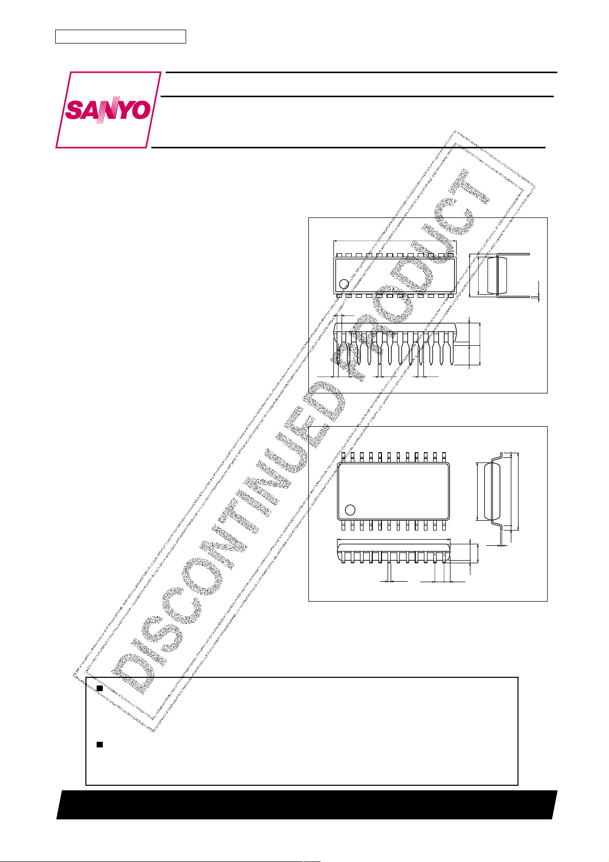
The LC74780 is available in 24-pin DIPs, and the
LC74780M, in 24-pin MFPs.
Features
• Complete text and graphics vide overlay circuitry.
• 128-character internal character generator ROM.
• 12 × 18-pixel characters.
• Three pixel widths and three pixel heights.
• Selectable background color.
• 8 colors at 4f
• 4 colors at 2fSC (NTSC)
• Built-in synchronization check and separation circuitry.
• Approximately 0.5 or 1 s period character flashing option.
• Screen blanking.
• NTSC, PAL and PAL-M format compatibility.
• 8-bit serial input format.
• 5V supply.
• 24-pin plastic DIP and 24-pin plastic MFP.
(NTSC/PAL/PAL-M)
SC
Package Dimensions
unit:mm
3067A-DIP24S
[LC74780]
21.0
24
1
0.9
(0.71)
1.78
unit:mm
3045B-MFP24
24
1
0.48
15.3
0.35
0.95
[LC74780M]
1.27
13
6.4
7.62
0.25
12
(3.25)
3.9max
3.3
0.51min
SANYO : DIP24S
13
7.9
12
2.15
0.1
0.67
SANYO : MFP24
0.15
2.5max
9.0
0.75
10.5
O1001TN (KT)/D1694TH(ID)/N1293JN No.4490–1/14
Page 2
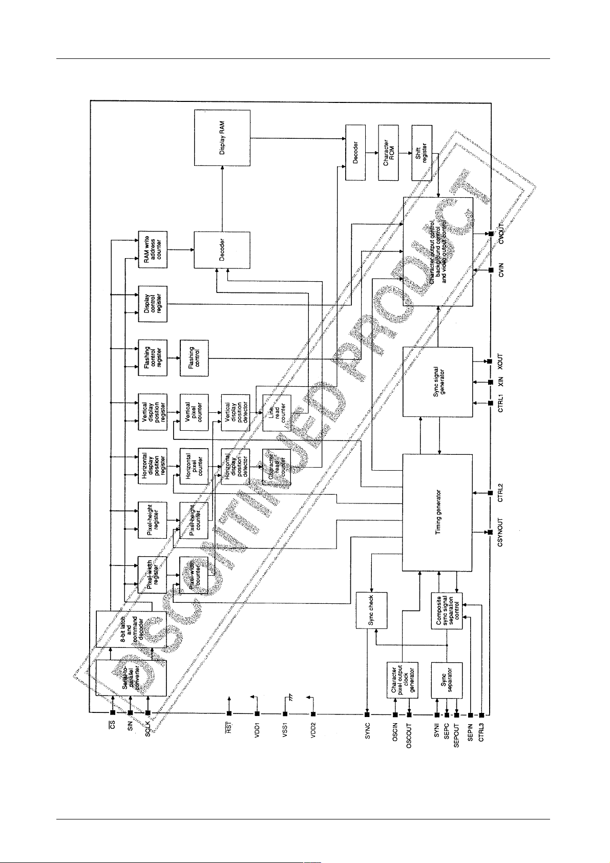
Block Diagram
LC74780, 74780M
No.4490–2/14
Page 3
Pin Functions
rebmuNemaNnoitpircseD
1V
2NIX
3TUOX
41LRTC
5TUONYSC
6NICSO .tuptuoretcarahcnoitarenegkcolclexiproftiucricCL.tupnirotallicsoCL
7TUOCSO .tuptuoretcarahcnoitarenegkcolclexiproftiucricCL.tuptuorotallicsoCL
8CNYS
9SC .)tupnisiseretsyh(ecnatsiserpu-lluphtiw,WOLnehwelbanetupniatadlaireS
01KLCS .)tupnisiseretsyh(ecnatsiserpu-lluphtiw,tupniatadlairesroftupnikcolC
11NIS .)tupnisiseretsyh(ecnatsiserpu-lluphtiw,tupniatadlaireS
21V
31TUOVC.tuptuolangisegamioedivetisopmoC
41CN.noitcennocoN
51NIVC.tupnilangisegamioedivetisopmoC
61V
71NICNYS
81CPES .desutonfinepoevaeL.noitcennocroticapacrotaludomtiucricnoitarapesnoitazinorhcnyS
91TUOPES
02NIPESVoteiT.tupnilangisnoitazinorhcnyslacitreV
122LRTC
223LRTC .HGIHnehwtupnitondna,WOLnehwlangistupniCNYSV.lortnoctupniNIPES
32TSR .)tupnisiseretsyh(ecnatsiserpu-lluphtiw,tupnitesermetsyS
42V
LC74780, 74780M
1SS
2DD
1DD
1DD
dnuorG
f2(tupnikcolclanretxerosnoitcennocroticapacrotallicsolatsyrclangiscnyslanretnI
f4ro
CS
.edom
.dnammocteserlanretniroftuptuooN.tuptuo
.dnammocteserlanretniroftuptuooN.tuptuosikcolclexip,)WOL
.)metsysgolanarof(noitaludomlevellangisegamioedivetisopmocrofylppusrewoP
.metsyslatigidrofylppusrewopV5
.langisnoitazinorhcnysetisopmocrolatnozirohlanretxenatupniotNICNYS
.desutonsinoitarapes
1DD
.metsyslatigidrofylppusrewopV5
.desutonfi
.WOLnehwdnammocybdetcelesM-LAP/LAP/CSTN
.HGIHnehwM-LAP.tupnitcelesdohtemnoitareneglangiscnysM-LAP/LAP/CSTN
.)
CS
rotallicsolatsyrcrofWOLdna,edomtupnikcolclanretxerofHGIH.tcelesedomtupnikcolC
sikcolcrotallicsolatsyrc,)WOLTSR(tesergniruD.tuptuolangisnoitazinorhcnysetisopmoC
TSR(tesergniruD.detcetedsicnysnehwHGIH.tuptuokcehclangisnoitazinorhcnyslanretxE
esu,desutonsitiucricnoitarapescnyslanretnifI.tupnitiucricnoitarapesnoitazinorhcnyS
cnyslanretnifilangisNICNYSstuptuO.tuptuotiucricnoitarapesnoitazinorhcnysetisopmoC
Specifications
Absolute Maximum Ratings at Ta = 25˚C
retemaraPlobmySsnoitidnoCsgnitaRtinU
V
Allowable Operating Ranges at Ta = –30 to +70˚C
Pin Assignment
Vdna
1DD
2DD
erutarepmetegarotSgtsT – 521+ot04
egatlovylppuscigoLV
egatlovylppusgolanAV
egatlovylppusV
stupnillarofegnaregatlovtupnIV
noitapissidrewopelbawollAxamdP52=aT °C053Wm
erutarepmetgnitarepOrpoT – 07+ot03
retemaraPlobmySsnoitidnoCsgnitaRtinU
egnaregatlovylppuscigoLV
egnaregatlovylppusgolanAV
DDxam
NIxam
egatlovtuptuoTUOPESdnaCNYS,TUONYSCV
TUOxam
1DD
2DD
1DD
2DD
VSS– Vot3.0
VSS– Vot3.0
VSS– Vot3.0
0.7+
SS
DD
DD
V72.1ot5.4
V
3.0+
V
3.0+
V
˚C
˚C
0.5V
0.5V
5.5ot5.4V
V
1DD
No.4490–3/14
Page 4
LC74780, 74780M
Electrical Characteristics at T a = –30 to +70˚C, V
retemaraPlobmySsnoitidnoC
V
1DD
V
2DD
tnerructupni
egatlov
egatlovtupni
egatlov
egatlovtupni
egatlovtupniNIXV
egatlovtuptuo
egatlovtuptuo
tnerrucylppuscigolI
tnerrucylppusgolanaI
tnerrucegakaeltupniNIVCI
tnerrucegakaeltuptuoTUOVCI
level-WOLNICSOdna3LRTC,2LRTC,1LRTC
2LRTC,NIPES,1LRTC,KLCS,NIS,SC,TSR
tnerructupnilevel-HGIH3LRTCdna
tupnilevel-WOLKLCSdnaNIS,SC,TSR
level-WOLNIPESdna3LRTC,2LRTC,1LRTC
tupnilevel-HGIHKLCSdnaNIS,SC,TSR
level-HGIHNIPESdna3LRTC,2LRTC,1LRTC
egatlovtupnioedivetisopmocNIVCV
egatlovtupnioedivetisopmocNICNYSV
level-WOLTUOPESdnaCNYS,TUONYSC
level-HGIHTUOPESdnaCNYS,TUONYSC
egatlovcnysTUOVCV
egatlovlatsedepTUOVCV
egatlovtsrubroloclevel-WOLTUOVCV
egatlovtsrubroloclevel-HGIHTUOVCV
egatlovrolocdnuorgkcablevel-WOLTUOVCV
egatlovrolocdnuorgkcablevel-HGIHTUOVCV
egatlovredrobTUOVCV
egatlovretcarahcTUOVCV
ecnatsiserpu-llupKLCSdnaNIS,SC,TSRR
ycneuqerfrotallicsoTUOXdnaNIXf
ycneuqerfrotallicsoTUOCSOdnaNICSOf
1DD
V
2DD
1kael
2kael
I
V
LI
I
V
HI
V
1LI
V
2LI
V
1HI
V
2HI
1NI
2NI
3NI
V
V
V
1LO
V
1HO
NS
DP
LBC
HBC
LSR
HSR
KB
AHC
UP
1CSO
2CSO
Notes
1. CV
2. CV
OUT
OUT
at V
at V
DD1=VDD2
DD1=VDD2
=5.0V, 0.8V sync level
=5.0V, 1.0V sync level
= 5V, unless otherwise noted
DD1
sgnitaR
nimpytxam
rotallicsoCLzHM8
V5=02Am
2DD
V
=NI
1SS
V
=NI
1DD
f,tupnikcolclanretxE
f2=
NI
5.4=,VI
1DD
5.4=,VIHO=– Am0.15.3V
1DD
.1etoneeS07.028.0
.2etoneeS59.070.1
.1etoneeS03.124.145.1V
.2etoneeS45.166.187.1V
.1etoneeS00.121.142.1V
.2etoneeS52.173.194.1V
.1etoneeS26.147.168.1V
.2etoneeS58.179.190.2V
.1etoneeS54.175.196.1V
.2etoneeS96.118.139.1V
.1etoneeS89.101.222.2V
.2etoneeS12.233.254.2V
.1etoneeS25.146.167.1V
.2etoneeS66.187.109.1V
.1etoneeS36.257.278.2V
.2etoneeS97.219.230.3V
f2(CSTN
)951.7zHM
CS
f4(CSTN
)813.41zHM
CS
f4(LAP
)437.71zHM
CS
f4(M-LAP
)203.41zHM
CS
rotallicsoCL5
Am0.1=
LO
f4ro
CS
,rotallicsolatsyrczHM951.7,nepostuptuollA
1– Aµ
VSS–
3.0
VSS–
3.0
V8.0
1DD
V7.0
1DD
CS
sniptasgnitteslanoitponosdnepeD5205
02.0
V2.0
V3.0
V
1DD
V
1DD
0.2V
0.2
51Am
1
1
1Aµ
1DD
1DD
3.0+
3.0+
5.2
V
0.5
V
0.1
49.0
91.1
09
01
tinU
Aµ
Aµ
V
V
V
V
P-P
P-P
P-P
V
V
V
KΩ
zHM
Timing Characteristics at Ta = –30 to +70˚C, V
retemaraPlobmySsnoitidnoC
htdiwesluptupniKLCSt
htdiwesluptupnilevel-HGIHSCt
emitputestupniSCt
emitputestupniatadNISt
emitdlohtupniSCt
emitdlohtupniatadNISt
emitetirwdrowatadtib-8t
emitetirwatadMARt
)KLCS(W
)SC(W
)SC(US
)NIS(US
)SC(H
)NIS(H
DROW
TW
= 5 ±0.5V
DD1
sgnitaR
nimpytxam
002sn
1sµ
002sn
002sn
2sµ
002sn
2.4sµ
1sµ
No.4490–4/14
tinU
Page 5
LC74780, 74780M
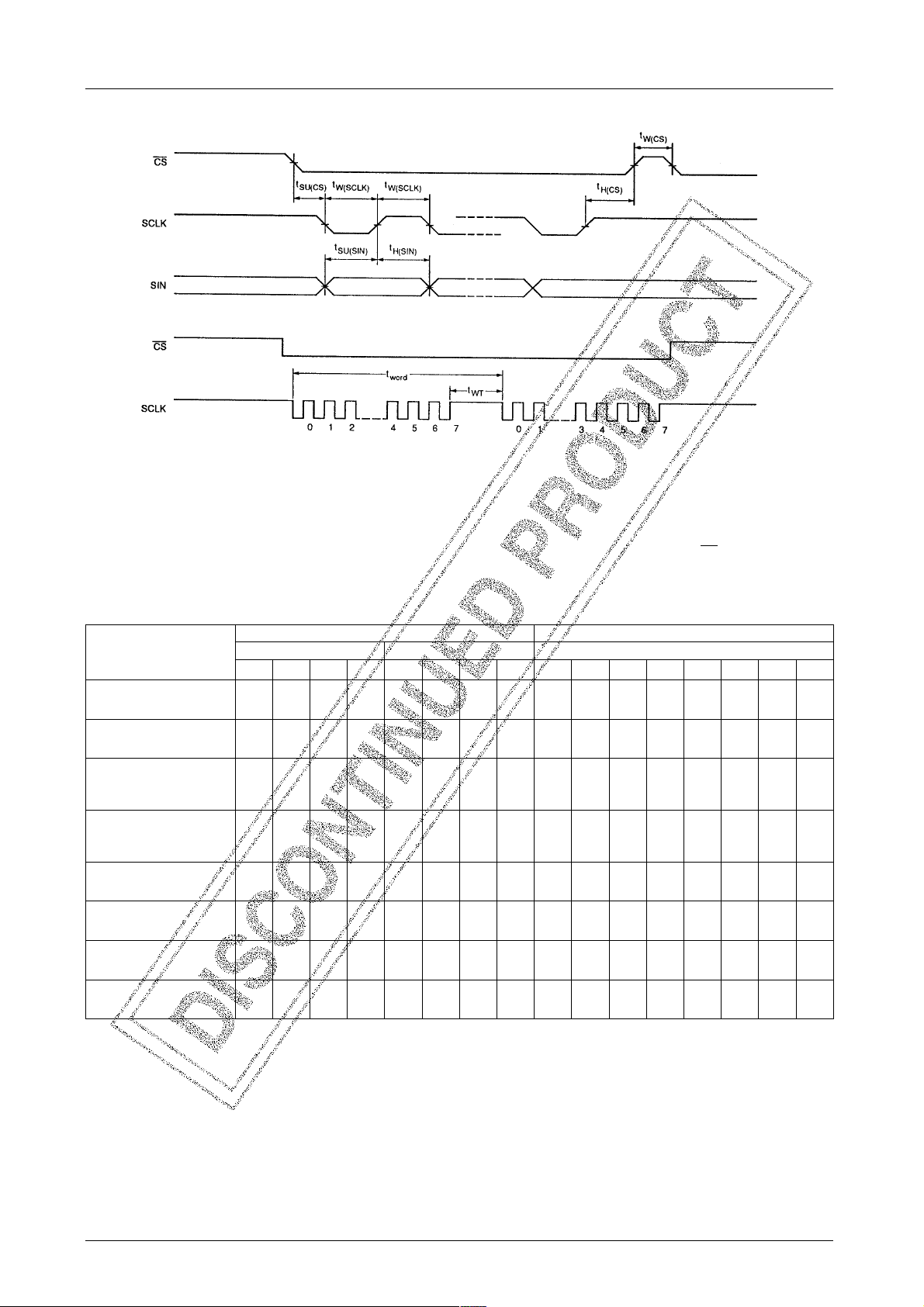
Serial Data Input Timing
Display Control Features and Characteristics
Display Control Command Structure
The display control commands, COMMAND0 to COMMAND7, are shifted in 8-bit serial units. The first byte of a
command consists of an identification code and data. The
second byte consists of data only . Once the command identification code in byte 1 has been written, it is saved until
Display Control Command Data
etybtsriFetybdnoceS
dnammoC
7654321076543210
0DNAMMOC
1DNAMMOC
dnammoc
2DNAMMOC
dnammoc
3DNAMMOC
dnammoc
4DNAMMOC
dnammoc
5DNAMMOC
dnammoc
6DNAMMOC
dnammocgnittes
7DNAMMOC
dnammoc
etirw)MARV(yromemyalpsiD
dnammocgnittessserdda
gnittesezisretcarahc
gnittesezisretcarahc
gnitteslortnocyalpsiD
gnitteslortnocyalpsiD
gnitteslortnocyalpsiD
1000 3V2V1V0V000 4H3H2H1H0H
etirwatadretcarahcyalpsiD
10010000 ta6C5C4C3C2C1C0C
dnanoitisopyalpsidlacitreV
10 10 12SV02SV11SV01SV0SF5PV4PV3PV2PV1PV0PV
dnanoitisopyalpsidlatnoziroH
10 11 12SH02SH11SH01SH0CL5PH4PH3PH2PH1PH0PH
1100
1101 1PN0PNNONTNI 000 LCBBC2HP1HP0HP
lortnoclangisnoitazinorhcnyS
1110
1111 1XE1DP0XE0DP
edocdnammoCatadgnirotsretsigerroataDatadgnirotsretsigerroataD
TST
DOM
1DOM0DOM
the next time the first byte is written. If COMMAND1 is
written, the display character write mode begins and the
first byte does not change. When CS is HIGH, COMMAND0 is set.
MAR
CSO
SRE
PTS
SID
NIL
SYS
02KLB1KLB0KLB1KB0KBVR
TSR
TUM0 2NR1NR0NR3NS2NS1NS0NS
PSD
NO
No.4490–5/14
Page 6

LC74780, 74780M
COMMAND0: Display Memory Write Address Setting Command
COMMAND0: first byte
ot0AD
7AD
00V
11V
22V
33V
40
50
60
71
emanretsigeR
sutatSnoitcnuF
0
1
0
1
0
1
0
1
COMMAND0: second byte
ot0AD
7AD
00H
11H
22H
33H
44H
50
60
70 tibnoitacifitnedietybdnoceS
emanretsigeR
sutatSnoitcnuF
0
1
0
1
0
1
0
1
0
1
Note
On system reset with RST, the status of all registers is set to 0.
stnetnoCretsigeR
HBot0sserddaenilyromemyalpsiD
edocnoitacifitnedi0DNAMMOC
stnetnoCretsigeR
H71ot0sserddayromemyalpsiD
skrameR
skrameR
COMMAND1: Display Character Data Write Command
COMMAND1: first byte
ot0AD
7AD
00
10
20
30
41
50
60
71
emanretsigeR
sutatSnoitcnuF
edocnoitacifitnedi1DNAMMOC
stnetnoCretsigeR
skrameR
yalpsid,tupnisidnammocretfA
tessiedometirwatadretcarahc
HGIHtessiSClitnu
No.4490–6/14
Page 7

LC74780, 74780M
COMMAND1: second byte
ot0AD
7AD
00C
11C
22C
33C
44C
55C
66C
7ta
emanretsigeR
sutatSnoitcnuF
0
1
0
1
0
1
0
1
0
1
0
1
0
1
0FFOetubirttaretcarahC
1NOetubirttaretcarahC
HF7ot0edocretcarahC
Note
On system reset with RST, the status of all registers is set to 0.
COMMAND2: Vertical Display Position and Character Size Setting Command
COMMAND2: first byte
ot0AD
7AD
001SV
111SV
202SV
312SV
40
51
60
71
emanretsigeR
sutatSnoitcnuF
0
1
0
1
0
1
0
1
11SV01SVthgieH
00 lexip/H1
01 lexip/H2
10 lexip/H3
11 lexip/H1
12SV02SVthgieH
00 lexip/H1
01 lexip/H2
10 lexip/H3
11 lexip/H1
stnetnoCretsigeR
stnetnoCretsigeR
edocnoitacifitnedi2DNAMMOC
skrameR
skrameR
ezisretcarahclacitreveniltsriF
ezisretcarahclacitrevenildnoceS
No.4490–7/14
Page 8

COMMAND2: second byte
ot0AD
7AD
0)BSL(0PV
emanretsigeR
LC74780, 74780M
sutatSnoitcnuF
0
1
stnetnoCretsigeR
ybdenimretednoitisopetanidrooclacitrevlaitinI
skrameR
11PV
22PV
33PV
44PV
5)BSM(5PV
6SF
70 tibnoitacifitnedietybdnoceS
0
1
0
1
0
1
0
1
0
1
0f2
1f4
doirepeslupnoitazinorhcnyslatnozirohehtsiHerehw
CS
CS
ycneuqerfrotallicsolatsyrc
ycneuqerfrotallicsolatsyrc
Note
On system reset with RST, the status of all registers is set to 0.
COMMAND3: Horizontal Display Position and Character Size Setting Command
COMMAND3: first byte
ot0AD
7AD
001SH
111SH
202SH
312SH
41
51
60
71
emanretsigeR
sutatSnoitcnuF
0
1
0
1
0
1
0
1
11SH01SHhtdiW
00 T1
01 T2
10 T3
11 T1
12SH02SHhtdiW
00 T1
01 T2
10 T3
11 T1
stnetnoCretsigeR
lexip/
C
lexip/
C
lexip/
C
lexip/
C
lexip/
C
lexip/
C
lexip/
C
lexip/
C
edocnoitacifitnedi3DNAMMOC
etanidrooclacitrevlaitiniehT
ot0PV,stib6nitessinoitisop
,0PV,BSLehterehw,5PV
H2otsdnopserroc
skrameR
ezisretcarahclatnoziroheniltsriF
ezis
retcarahclatnozirohenildnoceS
No.4490–8/14
Page 9

LC74780, 74780M
COMMAND3: second byte
ot0AD
7AD
0)BSL(0PH
11PH
22PH
33PH
44PH
5)BSM(5PH
6CL
70 tibnoitacifitnedietybdnoceS
Note
On system reset with RST, the status of all registers is set to 0.
COMMAND4: Display Control Setting Command
COMMAND4: first byte
ot0AD
7AD
0TSRSYS
1PTSCSO
2SREMAR
3DOMTST
40
50
61
71
emanretsigeR
emanretsigeR
sutatSnoitcnuF
0
1
0
1
0
1
0
1
0
1
0
1
0kcolctodrotallicsoCL
1kcolctodrotallicsolatsyrC
sutatSnoitcnuF
0
1FFOyalpsidehtsnrutdnasretsigerllasteseR
0elbasidpotsrotallicsoCLdnalatsyrC
1elbanepotsyrtiucricrotallicsoCLdnalatsyrC
0
1)HF7ottes(MARyalpsidsesarE
0edomgnitarepolamroN
1edomtseT
Terehw
C
doirep
edocnoitacifitnedi4DNAMMOC
stnetnoCretsigeR
ybnevigsinoitisopetanidrooclatnozirohlaitiniehT
noitalicsoedomnoitarepoTUOCSOdnaNICSOehtsi
noitcerid
stnetnoCretsigeR
yalpsid
skrameR
etanidrooclatnozirohlaitiniehT
ot0PH,stib6nitessinoitisop
,0PH,BSLehterehw,5PH
T2otsdnopserroc
C
ehtrofdesukcolctodehtstceleS
esrevsnartyalpsidretcarahc
skrameR
WOLseogSC
nehwsruccooslatesermetsysA
retcarahcedomcnyslanretxE
deriuqererasµ005yletamixorppA
)FFOyalpsidhtiw(MAResareot
detcelesebtondluohsedomtseT
noitarepolamrongnirud
COMMAND4: second byte
ot0AD
7AD
0NOPSD
1VR
20KB
31KB
40KLB
51KLB
62KLB
70 tibnoitacifitnedietybdnoceS
emanretsigeR
sutatSnoitcnuF
0FFOyalpsidretcarahC
1NOyalpsidretcarahC
0FFOsretcarahcesreveR
1NOsretcarahcesreveR
0FFOgniknilB
1NOgniknilB
0s5.0yletamixorppadoirepgniknilB
1s0.1yletamixorppadoirepgniknilB
0
1
0
1
0yalpsidretcarahC
1yalpsidoediV
1KLB0KLBtcelesgniknalB
00 FFOgniknalB
01 ezisretcarahC
10 ezisredroB
11 ezislluF
Note
On system reset with RST, the status of all registers is set to 0.
stnetnoCretsigeR
skrameR
,sretcarahcesrevnigniknilbnehW
neewtebetanretlasretcarahc
esrevnidnalamron
doirepgniknilbstceleS
ezisaeragniknalbehtstceleS
noitcelesezislluF
No.4490–9/14
Page 10

LC74780, 74780M
COMMAND5: Display Control Setting Command
COMMAND5: first byte
ot0AD
7AD
0TNI
1NON
20PN
31PN
41
50
61
71
COMMAND5: second byte
ot0AD
7AD
emanretsigeR
emanretsigeR
sutatSnoitcnuF
0noitazinorhcnyslanretxE
1noitazinorhcnyslanretnI
0decafretnI
1decafretni-noN
0
1
0
1
sutatSnoitcnuF
1PN0PNtcelesedoM
00 CSTN
01 M-LAP
10 LAP
11 CSTN
stnetnoCretsigeR
edocnoitacifitnedi5DNAMMOC
stnetnoCretsigeR
skrameR
dnalanretxeneewtebsehctiwS
noitazinorhcnyslanretni
dnadecalretnineewtebsehctiwS
decalretni-non
LAP,CSTNneewtebsehctiwS
sedomM-LAPdna
skrameR
0
00HP
1
0
11HP
1
0
22HP
1
3BC
4LCB
50
60
70 tibnoitacifitnedietybdnoceS
0tuptuosilangistsrubroloC
1detlahsituptuolangistsrubroloC
0tneserprolocdnuorgkcaB
1)tessiylnoleveldnuorgkcab(tneserptonrolocdnuorgkcaB
2HP1HP0HP
000
001 *esahpnIesahpnI
0103π *2/ π 2/
011
1003π 4/3±π4/
101
1107π 4/ π 4/
1115π 4/3π 4/
f2taCSTN*
CS
π *2/
π*
π 4/
Note
On system reset with RST, the status of all registers is set to 0.
COMMAND6: Synchronization Signal Control Setting Command
COMMAND6: first byte
ot0AD
7AD
0TUM
1NILSID
20DOM
31DOM
40
51
61
71
emanretsigeR
sutatSnoitcnuF
0tuptuolamroN
1levellatsedepehttadexifsiTUOVCdnatucsiNIVC
0senil21
1senil01
0langiscnysetisopmoC
1tuptuolangis-ROredrobdnaretcarahC
0langisnoitarapesnoitazinorhcnysetisopmoC
1cnyslanretniroftuptuolevel-HGIH
stnetnoCretsigeR
edocnoitacifitnedi6DNAMMOC
CSTNLAP
±π 2/
±π 4/
±π
esahprolocdnuorgkcaB
margaidesahp
1=LCBnehwseilppA
lanretnirofseilppA
ylnonoitazinorhcnys
skrameR
TUOVCsehctiwS
senil
TUONYSCsehctiwS
TUOPESsehctiwS
rolocdnuorgkcab,tsrubrolocLAP
yalpsidforebmunehtstceleS
No.4490–10/14
Page 11

LC74780, 74780M
COMMAND6: second byte
ot0AD
7AD
00NS
11NS
22NS
33NS
40NR
51NR
62NR
70 tibnoitacifitnedietybdnoceS
Note
On system reset with RST, the status of all registers is set to 0.
emanretsigeR
sutatSnoitcnuF
0
1
0
1
0
1
0
1
0
1
0
1
0
1
3NS2NS1NS0NSycneuqerfnoitceteD
0000 noitcetedoN
0001 semit23
0010 semit46
0100 semit821
1000 semit652
2NR1NR0NRycneuqerfnoitceteD
000 semit0
001 semit4
010 semit8
100 semit61
stnetnoCretsigeR
skrameR
noitcetedlangiscnyslanretxE
ehtnehwsenimretedlortnoc
.FFOotNOmorfseoglangis
ni,doirepgnilpmasehtstceleS
langiscnyslatnozirohehtfostinu
cnysehthcihwrof,)H1(elcyc
.detcetedebtonnacdnaseunitnoc
noitcetedlangiscnyslanretxE
ehtnehwsenimretedlortnoc
.NOotFFOmorfseoglangis
ni,doirepgnilpmasehtstceleS
langiscnyslatnozirohehtfostinu
cnysehthcihwrof,)H1(elcyc
.detcetedebnacdnaseunitnoc
COMMAND7: Display Control Setting Command
COMMAND7: first byte
ot0AD
7AD
00DP
10XE
21DP
31XE
41
51
61
71
emanretsigeR
sutatSnoitcnuF
0tuptuolevel-WOL
1tuptuolevel-HGIH
0tuptuosgnittes0EDOM
1tuptuosgnittes0ATADTROP
0tuptuolevel-WOL
1tuptuolevel-HGIH
0tuptuosgnittes1EDOM
1tuptuosgnittes1ATADTROP
edocnoitacifitnedi7DNAMMOC
Note
On system reset with RST, the status of all registers is set to 0.
stnetnoCretsigeR
skrameR
TUONYSCsehctiwS
TUOPESsehctiwS
No.4490–11/14
Page 12

LC74780, 74780M
Display Configuration
The display is 24 characters by 12 rows large. Up to 288
characters can be displayed, unless the character size is
expanded. The display memory address is set as a row ad-
dress in the range 0 to 11 and a column address in the range
0 to 23.
No.4490–12/14
Page 13

Composite Video Output
CVOUT Output Waveform (V
DD2
LC74780, 74780M
=5.00V)
levelegatlovtuptuOlobmyS)V(cnysV8.0taegatlovtuptuO)V(cnysV0.1taegatlovtuptuO
retcarahCV
rolocdnuorgkcablevel-HGIHV
tsrubroloclevel-HGIHV
rolocdnuorgkcablevel-WOLV
redroBV
latsedePV
tsrubroloclevel-WOLV
cnySV
AHC
HSR
HBC
LSR
KB
DP
LBC
NS
57.219.2
01.233.2
47.179.1
75.118.1
46.187.1
24.166.1
21.173.1
28.070.1
Note
=5.00V
V
DD2
No.4490–13/14
Page 14

LC74780, 74780M
Specifications of any and all SANYO products described or contained herein stipulate the performance,
characteristics, and functions of the described products in the independent state, and are not guarantees
of the performance, characteristics, and functions of the described products as mounted in the customer's
products or equipment. To verify symptoms and states that cannot be evaluated in an independent device,
the customer should always evaluate and test devices mounted in the customer's products or equipment.
SANYO Electric Co., Ltd. strives to supply high-quality high-reliability products. However, any and all
semiconductor products fail with some probability. It is possible that these probabilistic failures could
give rise to accidents or events that could endanger human lives, that could give rise to smoke or fire,
or that could cause damage to other property. When designing equipment, adopt safety measures so
that these kinds of accidents or events cannot occur. Such measures include but are not limited to protective
circuits and error prevention circuits for safe design, redundant design, and structural design.
In the event that any or all SANYO products(including technical data,services) described or
contained herein are controlled under any of applicable local export control laws and regulations,
such products must not be exported without obtaining the export license from the authorities
concerned in accordance with the above law.
No part of this publication may be reproduced or transmitted in any form or by any means, electronic or
mechanical, including photocopying and recording, or any information storage or retrieval system,
or otherwise, without the prior written permission of SANYO Electric Co. , Ltd.
Any and all information described or contained herein are subject to change without notice due to
product/technology improvement, etc. When designing equipment, refer to the "Delivery Specification"
for the SANYO product that you intend to use.
Information (including circuit diagrams and circuit parameters) herein is for example only ; it is not
guaranteed for volume production. SANYO believes information herein is accurate and reliable, but
no guarantees are made or implied regarding its use or any infringements of intellectual property rights
or other rights of third parties.
This catalog provides information as of October, 2001. Specifications and information herein are subject
to change without notice.
PS No.4490–14/14
 Loading...