

Page 1
Overview
The LC74763 and LC74763M are on-screen display
CMOS LSIs that superimpose text and low-level
graphics onto a TV screen (video signal) under the
control of a microcontroller. The display characters
have a 12 by 18 dots structure, and 128 characters are
provided.
Features
• Display structure: 12 lines by 24 characters (up to 288
characters)
• Maximum character display: Up to 288 characters
• Character configuration: 12 (W) by 18 (H) dots
structure
• Number of characters: 128 characters (128 plus space
2 fonts)
• Character sizes: Three sizes (normal, double, and
triple sizes)
• Display starting positions: 64 horizontal and 64
vertical locations
• Reverse video function: Characters can be inverted on
a per character basis.
• Flashing types: Two types with periods of 0.5 and 1.0
second on a per character basis (duty fixed at 50%)
• Background color: One of eight colors (when internal
synchronization used)
• External control input: Serial data input in 8-bit units
• Built-in horizontal/vertical sync separation circuit,
AFC circuit, and synchronization detector
• Video output: Composite video signal output in
NTSC, PAL, PAL-M, PAL-N, PAL60, NTSC4.43, or
SECAM format
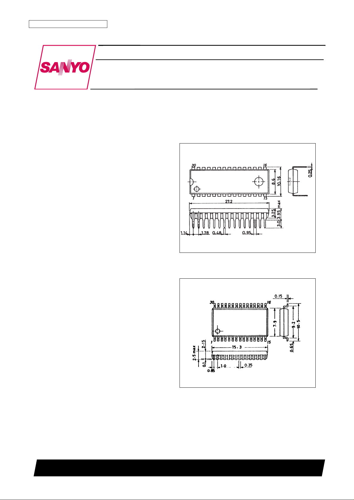
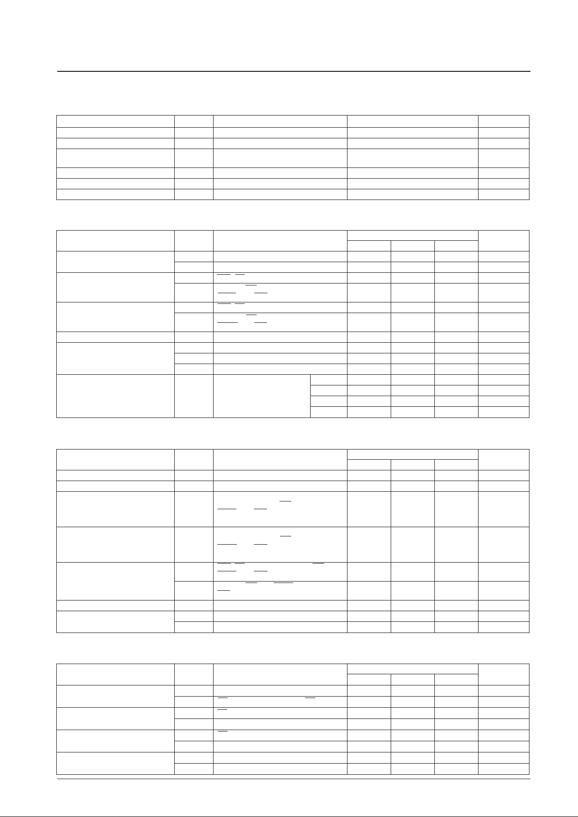
Package Dimensions
unit: mm
3196-DIP30SD
unit: mm
3216A-MFP30S
Preliminary
[LC74763M]
SANYO: MFP30S
[LC74763]
SANYO: DIP30SD
CMOS IC
Ordering number : *EN5039
32095TH (OT) No. 5039-1/19
LC74763, 74763M
SANYO Electric Co.,Ltd. Semiconductor Bussiness Headquarters
TOKYO OFFICE Tokyo Bldg., 1-10, 1 Chome, Ueno, Taito-ku, TOKYO, 110-8534 JAPAN
On-Screen Display LSI
Page 2
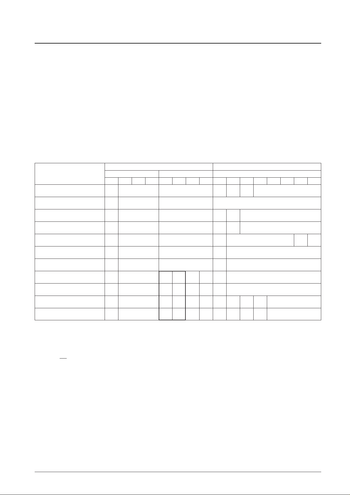
Specifications
Absolute Maximum Ratings at Ta = 25°C
Parameter Symbol Conditions Ratings Unit
Maximum supply voltage V
DD
max V
DD1
, V
DD2
pins VSS– 0.3 to VSS+ 7.0 V
Maximum input voltage V
IN
max All input pins VSS– 0.3 to VDD+ 0.3 V
Maximum output voltage V
OUT
max
HSYNC
OUT
, VSYNC
OUT
,
V
SS
– 0.3 to VDD+ 0.3 V
SYNC
DET
pins
Allowable power dissipation Pd max 300 mW
Operating temperature Topr –30 to +70 °C
Storage temperature Tstg –40 to +125 °C
Allowable Operating Ranges at Ta = –30 to +70°C
Ratings
Parameter Symbol Conditions
min typ max
Unit
Supply voltage
V
DD1
V
DD1
pin 4.5 5.0 5.5 V
V
DD2
V
DD2
pin 4.5 5.0 1.27 V
DD1
V
Input high level voltage
V
IH1
RST, CS, SIN, SCLK pins 0.8 V
DD1
V
DD1
+ 0.3 V
V
IH2
SECAM, 525/625,
0.7 V
DD1
V
DD1
+ 0.3 V
NTSC/PAL, 3.58/4.43 pins
Input low level voltage
V
IL1
RST, CS, SIN, SCLK VSS– 0.3 0.2 V
DD1
V
V
IL2
SECAM, 525/625,
VSS– 0.3 0.3 V
DD1
V
NTSC/PAL, 3.58/4.43 pins
Input voltage V
IN
FC, AMPINpins VSS– 0.3 V
DD1
+ 0.3 V
V
IN1
CVIN pins 2 V
PP
V
Composite video signal input voltage V
IN2
CVCRpins 2 V
PP
V
V
IN3
SYNCINpins 2 V
PP
2.5 V
PP
V
Oscillator frequency
NTSC 14.318 MHz
F
OSC1
Xtal
IN1
, Xtal
OUT1
, Xtal
IN2
,
PAL 17.734 MHz
Xtal
OUT2
pins; 4fsc
PAL-M 14.302 MHz
PAL-N 14.328 MHz
Electrical Characteristics at Ta = –30 to +70°C, with V
DD1
= V
DD2
= 5 V unless otherwise specified
Ratings
Parameter Symbol Conditions
min typ max
Unit
Output off leakage current I
leak1
CV
OUT
pin 10 µA
Input off leakage current I
leak2
CVIN, CVCRpins 10 µA
Output high level voltage V
OH
HSYNC
OUT
, VSYNC
OUT
,
3.5 V
SYNC
DET
, SECAM, 525/625,
NTSC/PAL, 3.58/4.43, AMP
OUT
,
PD
OUT
pins; V
DD1
= 4.5 V, IOH= –1.0 mA
Output low level voltage V
OL
HSYNC
OUT
, VSYNC
OUT
,
1.0 V
SYNC
DET
, SECAM, 525/625,
NTSC/PAL, 3.58/4.43, AMP
OUT
,
PD
OUT
pins; V
DD1
= 4.5 V, IOL= 1.0 mA
Input current
I
IH
RST, CS, SIN, SCLK, SECAM, 525/625,
1 µA
NTSC/PAL, 3.58/4.43 pins; V
IN
= V
DD1
I
IL
SECAM, 525/625, NTSC/PAL,
–1 µA
3.58/4.43 pin; V
IN
= V
SS1
Oscillator frequency F
OSC3
VCOIN, VCO
OUT
pins; FC = 1/2 V
DD1
14.12 MHz
Operating current dissipation
I
DD1
V
DD1
pin; All outputs open, Xtal: 4fsc 15 mA
I
DD2
V
DD2
pin; V
DD2
= 5.0 V 20 mA
Timing Characteristics at Ta = –30 to +70°C, VDD= 5 ±0.5 V
Ratings
Parameter Symbol Conditions
min typ max
Unit
Minimum input pulse width
t
W(SCLK)
SCLK pin 200 ns
t
W(CS)
CS pin (during periods when CS is high) 1 µs
Data setup time
t
SU(CS)
CS pin 200 ns
t
SU(SIN)
SIN pin 200 ns
Data hold time
t
h(CS)
CS pin 2 µs
t
h(SIN)
SIN pin 200 ns
One word write time
t
word
Write time for 8 bits of data 4.2 µs
t
wt
RAM data write time 1 µs
LC74763, 74763M
No. 5039-2/19
Page 3
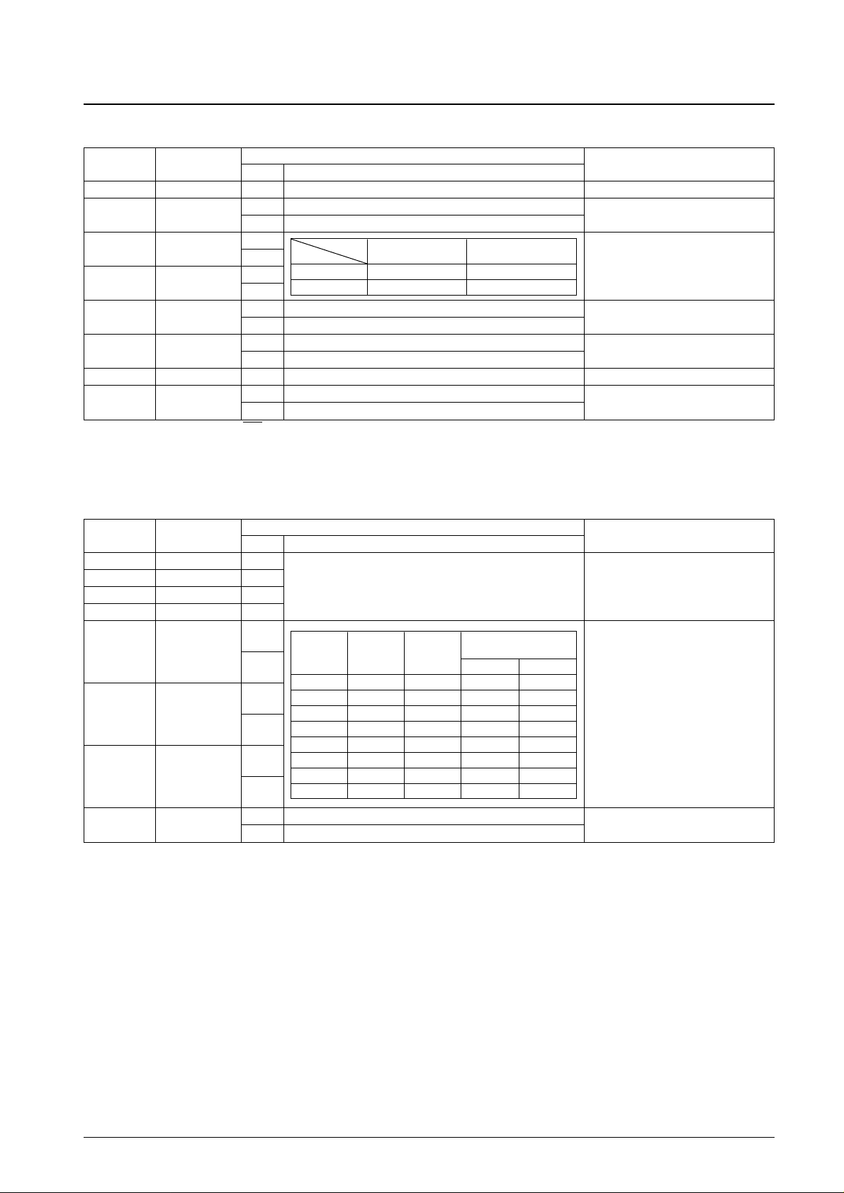
Pin Functions
Pin No. Symbol Function Description
1 V
SS
Ground Ground connection
2 Xtal
IN1
Crystal oscillator connection
Connection for the crystal and capacitor used to form the crystal oscillator that generates
3 Xtal
OUT1
the internal synchronization signal. The oscillator can be selected with a command switch.
4 HSYNC
OUT
Horizontal synchronization Outputs the horizontal synchronization signal (AFC). The output polarity can be selected
output (metal option). Also functions as general output port (command switch).
5 Xtal
IN2
Crystal oscillator connection
Connection for the crystal and capacitor used to form the crystal oscillator that generates
6 Xtal
OUT2
the internal synchronization signal.
7 VSYNC
OUT
Vertical synchronization output
Outputs the vertical synchronization signal. The output polarity can be selected (metal
option). Also functions as general output port (command switch).
8 CS Enable input
Enables/disables serial data input. Serial data is enabled when this pin is low (hysteresis
input). Pull-up resistor built in (metal option).
9 SIN Data input Serial data input (hysteresis input). Pull-up resistor built in (metal option).
10 SCLK Clock input Clock input for serial data input (hysteresis input). Pull-up resistor built in (metal option).
SECAM mode switch input/
During input, switches between SECAM and other modes.
11 SECAM
output (command switch)
During output, functions as general output port or internal V output (command switch).
Low = other modes, high = SECAM mode
525/625 switch input/output
During input, switches between 525 scan lines and 625 scan lines.
12 525/625
(command switch)
During output, functions as general output port or character data output (command switch).
Low = 525 lines, high = 625 lines
NTSC/PAL switch input/output
Switches the color mode between NTSC and PAL.
13 NTSC/PAL
(command switch)
During output, functions as general output port or frame data output (command switch).
Low = NTSC, high = PAL
Switch FSC between 3.58 MHz and 4.43 MHz.
14 3.58/4.43 3.58/4.43 switch input/output During output, functions as general output port or halftone output (command switch).
(command switch) Low = 3.58, high = 4.43
15 RST Reset input
System reset input pin, low is active (hysteresis input).
Pull-up resistor built in (metal option).
16 CV
OUT
Video signal output Composite video output
17 V
DD2
Power supply connection Power supply connection for composite video signal level generation
18 CV
IN
Video signal input Composite video input
19 CV
CR
Video signal input SECAM chroma signal input
20 SYNC
IN
Sync separator circuit input Built-in sync separator circuit video signal input
21 SEP
C
Sync separator circuit Built-in sync separator circuit
22 V
SS
Ground Ground connection
23 PD
OUT
Control voltage output AFC control voltage output
24 AMP
IN
AFC filter connection Filter connection
25 AMP
OUT
26 FC Control voltage input AFC control voltage input
27 VCO
IN
LC oscillator connection VCO LC oscillator circuit coil and capacitor connection
28 VCO
OUT
External synchronization signal
Outputs the exclusive NOR of the horizontal synchronization signal (AFC) and CSYNC (sync
29 SYNC
DET
detection output
separator). The output polarity can be selected (metal option). Also functions as general
output port (command switch).
30 V
DD1
Power supply connection Power supply connection (+5 V: digital system power supply)
LC74763, 74763M
No. 5039-3/19
Page 4

LC74763, 74763M
Pin Assignment
Serial Data Input Timing
No. 5039-4/19
Top view
Page 5
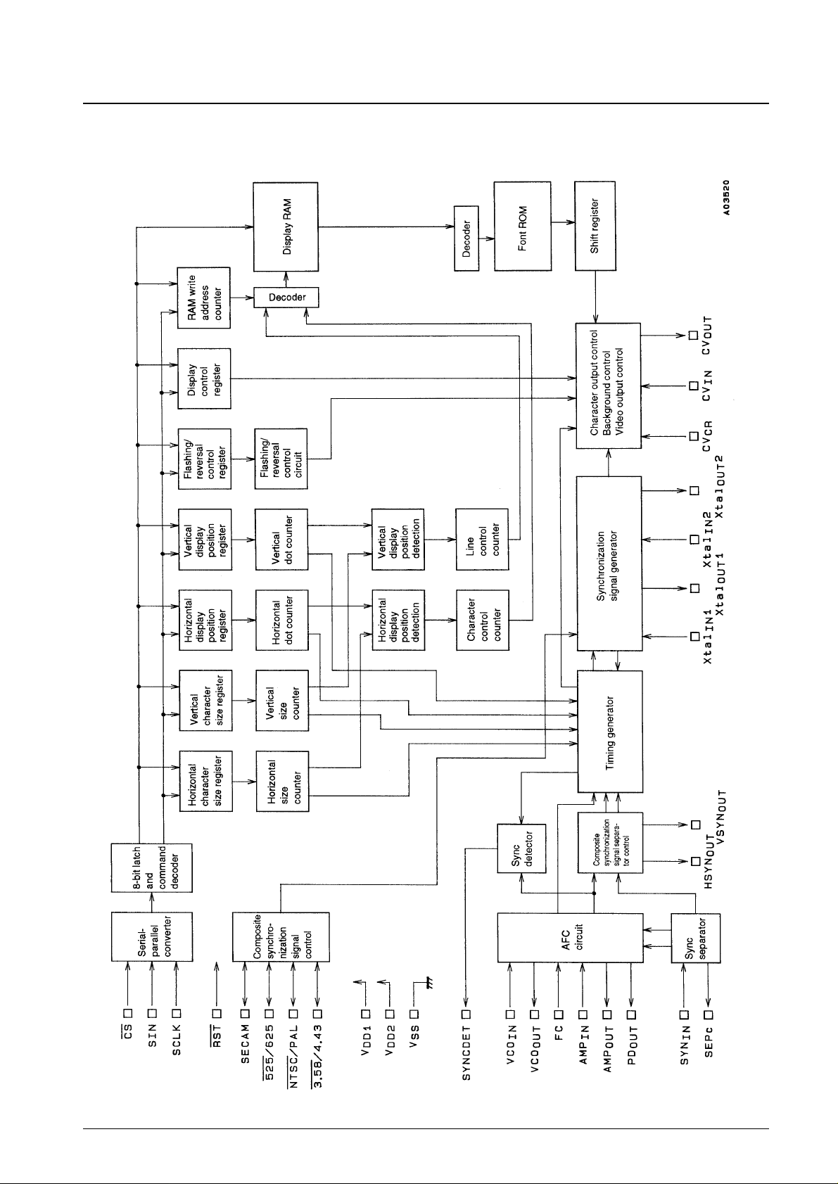
System Block Diagram
LC74763, 74763M
No. 5039-5/19
Page 6
LC74763, 74763M
Display Control Commands
Display control commands are input in an 8-bit serial format. Commands consist of a command identification code in the
first byte and data in the second and following bytes. The following commands are supported.
① COMMAND0: Display memory (VRAM) write address setting command
➁ COMMAND1: Display character data write command
③ COMMAND2: Vertical display start position and character size (lines 1 and 2) setting command
➃ COMMAND3: Horizontal display start position and character size (lines 9 and 11) setting command
➄ COMMAND4: Display control setting command 1
➅ COMMAND5: Display control setting command 2
⑦ COMMAND6: Display control setting command 3
⑧ COMMAND7: Display control setting command 4
Display Control Command Tab le
First byte Second byte
Command
Command identification code
Data Data
7 6 5 4 3 2 1 0 7 6 5 4 3 2 1 0
COMMAND0 1 0 0 0 V3 V2 V1 V0 0 0 0 H4 H3 H2 H1 H0
Write address
COMMAND1 1 0 0 1 0 0 at2 at1 c7 c6 c5 c4 c3 c2 c1 c0
Character write
COMMAND2 1 0 1 0 SZ SZ SZ SZ 0 0 VP VP VP VP VP VP
Vertical display start position 21 20 11 10 5 4 3 2 1 0
COMMAND3 1 0 1 1 SZ SZ SZ SZ 0 0 HP HP HP HP HP HP
Horizontal display start position B1 B0 91 90 5 4 3 2 1 0
COMMAND4 1 1 0 0 RST RAM OSC RND 0 I/N BLK BLK BK ATS 0 DSP
Display control 1 1 0 1
COMMAND5 1 1 0 1 PH PH PH I/E 0 TST CHAL BKL RSL RSL CVM XTS
Display control 2 2 1 0 1 0
COMMAND6 1 1 1 0 MOD MOD MOD MOD 0 HFI M30S SMS IOS BCL BCL CB
Display control 3 3 2 1 0 1 0
COMMAND70 1 1 1 1 0 0 0 LINS 0 VCOS LIN LIN LIN LIN LIN LIN
Display control 4 1 5 4 3 2 1 0
COMMAND71 1 1 1 1 0 1 0 LINS 0 EG PS PS VMN SVIS VNS VSS
Display control 5 2 2 1
COMMAND72 1 1 1 1 1 0 0 LINS 0 0 0 0 MOD MOD MOD MOD
Display control 6 3 2 1 0
COMMAND73 1 1 1 1 1 1 0 LINS 0 0 0 0 VCOS SOUT VOUT
HOUT
Display control 7 2
Once the command identification code in the first bite is written, it is stored internally until the first byte of the following
command is written. However, when the display character data write command (COMMAND1) is written, the system
becomes locked in display character data write mode, and the first byte cannot be overwritten.
When the CS pin is set high the command state is set to COMMAND0, i.e., display memory write address setting mode.
No. 5039-6/19
Page 7

① COMMAND0: Display Memory Write Address Setting Command
First data byte
Register content
DA0 to DA7 Register name
State Function
Note
7 — 1
6 — 0
The command 0 identification code:
5 — 0 sets the display memory write address.
4 — 0
3 V3
0
1
2 V2
0
1
Display memory line address (from 0 to B (hexadecimal))
1 V1
0
1
0 V0
0
1
Second byte
Register content
DA0 to DA7 Register name
State Function
Note
7 — 0 Second byte identification code
6 — 0
5 — 0
4 H4
0
1
3 H3
0
1
2 H2
0
Display memory character address (from 0 to 17 (hexadecimal))
1
1 H1
0
1
0 H0
0
1
Note: When the chip is reset by the RST pin, the register states (bits) are all cleared to 0.
➁ COMMAND1: Display Character Data Write Setting Command
First byte
Register content
DA0 to DA7 Register name
State Function
Note
7 — 1
When this command is entered, the
6 — 0
The command 1 identification code:
chip locks in display character write
5 — 0 sets the display memory write address.
mode until the CS pin is set high.
4 — 1
3 — 0
2 — 0
1 at2
0 Turns character attribute 2 off.
Specifies highlight or flashing.
1 Turns character attribute 2 on.
0 at1
0 Turns character attribute 1 off.
Specifies reverse video.
1 Turns character attribute 1 on.
LC74763, 74763M
No. 5039-7/19
Page 8

Second byte
Register content
DA0 to DA7 Register name
State Function
Note
7 c7
0
1
6 c6
0
1
5 c5
0
1
4 c4
0
1
Character code (from 00 to 7F, FE, FF)
3 c3
0
1
2 c2
0
1
1 c1
0
1
0 c0
0
1
Note: When the chip is reset by the RST pin, the register states (bits) are all cleared to 0.
③ COMMAND2: Vertical Display Position Setting Command
First byte
Register content
DA0 to DA7 Register name
State Function
Note
7 — 1
6 — 0
The command 2 identification code:
5 — 1 sets the vertical display position.
4 — 0
3 SZ21
0
1
Character size for the second line
2 SZ20
0
1
1 SZ11
0
1
Character size for the first line
0 SZ10
0
1
Second byte
Register content
DA0 to DA7 Register name
State Function
Note
7 — 0 Second byte identification code
6 — 0
5
VP5 0 The vertical display start position is given by
(MSB)
1
4 VP4
0
1 where H is the horizontal synchronization pulse period.
3 VP3
0
The six bits VP0 to VP5 specify the
1
vertical display start position.
2 VP2
0 The weight of the lsb is 1
× H.
1
1 VP1
0
1
0
VP0 0
(LSB)
1
Note: When the chip is reset by the RST pin, the register states (bits) are all cleared to 0.
LC74763, 74763M
No. 5039-8/19
SZ20
SZ21
0 1
0 Normal size Double size
1 Triple size Normal size
SZ10
SZ11
0 1
0 Normal size Double size
1 Triple size Normal size
5
VS = H × ( Σ 2nVPn)
n = 0
Page 9

➃ COMMAND3: Horizontal Display Position Setting Command
First byte
Register content
DA0 to DA7 Register name
State Function
Note
7 — 1
6 — 0
The command 3 identification code:
5 — 1 sets the horizontal display position.
4 — 1
3 SZB1
0
1
The character size for the eleventh line.
2 SZB0
0
1
1 SZ91
0
1
The character size for the ninth line.
0 SZ90
0
1
Second byte
Register content
DA0 to DA7 Register name
State Function
Note
7 — 0 Second byte identification code
6 — 0
5
HP5 0
(MSB)
1
4 HP4
0
1
The horizontal display start position is given by
3 HP3
0 The six bits HP0 to HP5 specify the
1
vertical display start position.
2 HP2
0
The weight of the lsb is 1 x Tc.
1
where Tc is the period of the OSCIN and OSCOUT oscillator in
1 HP1
0
operating mode.
1
0
HP0 0
(LSB)
1
Note: When the chip is reset by the RST pin, the register states (bits) are all cleared to 0.
➄ COMMAND4: Display Control Setting Command 1
First byte
Register content
DA0 to DA7 Register name
State Function
Note
7 — 1
6 — 1
The command 4 identification code:
5 — 0 sets display control parameters.
4 — 0
3 RST
SYS
0 This reset occurs when the CS pin goes
1 Resets all registers. (Clears all registers to 0.)
low, and the reset state cleared when
the CS pin goes high.
2 RAM
ERS
0 The RAM erase function requires at
1 Erases display RAM. (Sets display RAM to FF (hexadecimal).)
least 500 µs.
It is executed on DSPOFF.
1 OSC
STP
0 Continues crystal oscillator operation. Only valid with character display off if
1 Stops the crystal oscillator.
external synchronization is used.
0 RND
SEL
0 Turns off rounding. Only valid for double and triple size
1 Turns on rounding.
characters.
LC74763, 74763M
No. 5039-9/19
SZB0
SZB1
0 1
0 Normal size Double size
1 Triple size Normal size
SZ90
SZ91
0 1
0 Normal size Double size
1 Triple size Normal size
5
HS = Tc × ( Σ 2nHPn)
n = 0
Page 10
LC74763, 74763M
Second byte
Register content
DA0 to DA7 Register name
State Function
Note
7 — 0 Second byte identification code
6 INT/NON
0 Interlaced Switches between interlaced and
1 Non-interlaced
non-interlaced display.
5 BLK1
0
1
Changes the blanking size.
4 BLK0
0
1
3 BK1
0 Flashing period about 0.5 s
Sets the flashing period.
1 Flashing period about 1 s
2 ATS
0 Highlight function
Selects at2.
1 Flashing function
1 — 0
0 DSPON
0 Character display off
Turns character output on and off.
1 Character display on
Note: When the chip is reset by the RST pin, the register states (bits) are all cleared to 0.
➅ COMMAND5: Display Control Setting Command 2
First byte
Register content
DA0 to DA7 Register name
State Function
Note
7 — 1
6 — 1
The command 5 identification code:
5 — 0 sets display control parameters.
4 — 1
3 PH2
0
1
2 PH1
0 Sets the phase of the background color
1
for color burst.sz
1 PH0
0
1
0 INT/EXT
0 External synchronization mode Switches between internal and external
1 Internal synchronization mode
synchronization.
No. 5039-10/19
BLK0
BLK1
0 1
0 Blanking off Character size blanking
1 Frame size blanking Total area blanking
Background color
(phase)
PHASE 2 PHASE 1 PHASE 0
NTSC PAL
0 0 0 π/2 ±π/2
0 0 1 In phase In phase
0 1 0 3 π/2 π/2
0 1 1 π ±π
1 0 0 3 π/4 ±3 π/4
1 0 1 π/4 ±π/4
1 1 0 7 π/4 π/4
1 1 1 5 π/4 3 π/4
±
±
±
Page 11

Second byte
Register content
DA0 to DA7 Register name
State Function
Note
7 — 0 Second byte identification code
6 TST
0 Normal operation Test mode should not be used. This bit
1 Test mode
should always be zero.
5 CHAL
0 Sets the character intensity level to about 85 IRE (bright white).
Switches the character intensity level.
1
Sets the character intensity level to about 72 IRE (white with a
touch of grey).
4 BKL
0
Sets the blanking intensity level to about 3 IRE (a deep black
Switches the blanking intensity level.
as a frame level).
1
Sets the blanking intensity level to about 13 IRE (a dark grey
as a frame level).
3 RSL1
0
1
Switches the background intensity level.
2 RSL0
0
1
1 CV
outmt
0 Normal CV
out
output
1 CV
out
pedestal level output
0 XTAL
sel
0 Selects XTAL1
Switches the oscillator circuit
1 Selects XTAL2
Note: When the chip is reset by the RST pin, the register states (bits) are all cleared to 0.
⑦ COMMAND6: Display Control Setting Command 3
First byte
Register content
DA0 to DA7 Register name
State Function
Note
7 — 1
6 — 1
The command 6 identification code:
5 — 1 sets display control parameters.
4 — 0
3 MOD3
0 Sets Fsc to 3.58 MHz. The logical or of this bit and the Fsc
1 Sets Fsc to 4.43 MHz.
switching input pin (pin 14) is used.
2 MOD2
0 Sets the color mode to NTSC. The logical or of this bit and the color
1 Sets the color mode to PAL.
mode switching input pin (pin 13) is
used.
1 MOD1
0 Sets the number of scan lines to 525 lines. The logical or of this bit and the scan
1 Sets the number of scan lines to 625 lines.
line count switching input pin (pin 12) is
used.
0 MOD0
0 Sets the mode to a mode other than SECAM. The logical or of this bit and the mode
1 Sets the mode to SECAM mode.
switching input pin (pin 11) is used.
LC74763, 74763M
No. 5039-11/19
RSL1 RSL0 Intensity level Amplitude
0 0 About 15 IRE About 60 IRE
0 1 About 30 IRE About 60 IRE
1 0 About 45 IRE About 60 IRE
1 1 About 55 IRE About 65 IRE
Page 12

Second byte
Register content
DA0 to DA7 Register name
State Function
Note
7 — 0 Second byte identification code
6
HALF
0 Normal mode
INT
1 Half internal synchronous mode
5
P14OUT
0 Halftone output
Selects P14 (3.58/4.43) output.
SEL
1 High output in internal synchronous mode
4
SECAM
0 In SECAM mode, only the character frame area is on.
Selects the CVCR “on” period.
SEL
1 In SECAM mode, the entire character display area is on.
3 IOS
0 Sets the mode setting pin to be an input pin. Switches the input/output direction of
1 Sets the mode setting pin to be an output pin.
the mode setting pins.
2 BCOL1
0
Determines whether a background color
1
is displayed. (Only valid in internal
1 BCOL0
0 synchronization mode.)
1
0 CBOFF
0 Outputs a color burst signal. Only valid when either BCOL0 is 1 or
1 Stops the output of color burst signals.
BCOL1 is 1.
Note: When the chip is reset by the RST pin, the register states (bits) are all cleared to 0.
⑧ COMMAND70: Display Control Setting Command 4
First byte
Register content
DA0 to DA7 Register name
State Function
Note
7 — 1
6 — 1
The command 7 identification code:
5 — 1 sets display control parameters.
4 — 1
3 — 0
Expansion command 0 identification code
2 — 0
1 — 0
0 LINS
0 Selects the lower 6 bits (bits 0 to 5) Selects the upper or lower six bits when
1 Selects the upper 6 bits (bits 6 to B)
halftone output line mode is specified.
Second byte
Register content
DA0 to DA7 Register name
State Function
Note
7 — 0 Second byte identification code
6
VCO
0 VCO frequency is 14.12 MHz
Selects VCO oscillation frequency.
SELECT1
1 VCO frequency is 7.07 MHz
5 LIN5
0 Turns off (low) sixth line halftone output. Used for the line 12 setting when LINS
1 Turns on (high) sixth line halftone output.
is high.
4 LIN4
0 Turns off (low) fifth line halftone output. Used for the line 11 setting when LINS
1 Turns on (high) fifth line halftone output.
is high.
3 LIN3
0 Turns off (low) fourth line halftone output. Used for the line 10 setting when LINS
1 Turns on (high) fourth line halftone output.
is high.
2 LIN2
0 Turns off (low) third line halftone output. Used for the line 9 setting when LINS is
1 Turns on (high) third line halftone output.
high.
1 LIN1
0 Turns off (low) second line halftone output. Used for the line 8 setting when LINS is
1 Turns on (high) second line halftone output.
high.
0 LIN0
0 Turns off (low) first line halftone output. Used for the line 7 setting when LINS is
1 Turns on (high) first line halftone output.
high.
Note: When the chip is reset by the RST pin, the register states (bits) are all cleared to 0.
LC74763, 74763M
No. 5039-12/19
BCOL1 BCOL0 Background color
0 0 Background color displayed
0 1 No background color (about 13 IRE)
1 0 No background color (about 23 IRE)
1 1 CV
outmt2
(CSYNC)
Page 13

➈ COMMAND71: Display Control Setting Command 5
First byte
Register content
DA0 to DA7 Register name
State Function
Note
7 — 1
6 — 1
The command 7 identification code: sets display
5 — 1
control parameters
4 — 1
3 — 0
Expansion command 1 identification code
2 — 1
1 — 0
0 LINS
0 Selects lower 6 bits (0 to 5).
Selects lower or upper 6 bits for half-
1 Selects upper 6 bits (6 to B).
tone output line setting.
Second byte
Register content
DA0 to DA7 Register name
State Function
Note
7 — 0 Second byte identification bit
6
EGMODE
0 Normal display
2SELECT
1 Applies frame to inverted characters also.
5
PORTSET
0 Sets port output data
SELECT2
1 Sets port (output switching)
4
PORTSET
0 Sets port output data
SELECT1
1 Sets port (output switching)
3
VMN
0 Normal V signal
SEL
1 VMASK signal
2 VINPsel
0 Normal I/O
1 V is input from P11.
1 VNPsel
0 V rise detection
Selects V detection polarity.
1 V fall detection
0 VSEPsel
0 VSEP is about 9.3 µs.
Selects V separation time.
1 VSEP is about 18.6 µs.
Note: When the chip is reset by the RST pin, the register states (bits) are all cleared to 0.
➉ COMMAND72: Display Control Setting Command 6
First byte
Register content
DA0 to DA7 Register name
State Function
Note
7 — 1
6 — 1
The command 7 identification code: sets display
5 — 1
control parameters
4 — 1
3 — 1
Expansion command 2 identification code
2 — 0
1 — 0
0 LINS
0 Selects lower 6 bits (0 to 5).
Selects lower or upper 6 bits for half-
1 Selects upper 6 bits (6 to B).
tone output line setting.
LC74763, 74763M
No. 5039-13/19
Page 14

LC74763, 74763M
Second byte
Register content
DA0 to DA7 Register name
State Function
Note
7 — 0 Second byte identification bit
6 — 0
5 — 0
4 — 0
3
MOD3
0 Normal MOD3 (P14) output (PS1 = 1)
Specifies port output data
SEL
1 Specifies MOD3 general port output
when PS1 = 0.
2
MOD2
0 Normal MOD2 (P13) output (PS1 = 1)
Specifies port output data
SEL
1 Specifies MOD2 general port output
when PS1 = 0.
1
MOD1
0 Normal MOD1 (P12) output (PS1 =1)
Specifies port output data
SEL
1 Specifies MOD1 general port output
when PS1 = 0.
0
MOD0
0 Normal MOD0 (P11) output (PS1 = 1)
Specifies port output data
SEL
1 Specifies MOD0 general port output
when PS1 = 0.
Note: When the chip is reset by the RST pin, the register states (bits) are all cleared to 0.
11
COMMAND73: Display Control Setting Command 7
First byte
Register content
DA0 to DA7 Register name
State Function
Note
7 — 1
6 — 1
The command 7 identification code: sets display
5 — 1
control parameters
4 — 1
3 — 1
Expansion command 3 identification code
2 — 1
1 — 0
0 LINS
0 Selects lower 6 bits (0 to 5).
Selects lower or upper 6 bits for half
1 Selects upper 6 bits (6 to B).
tone output line setting.
Second byte
Register content
DA0 to DA7 Register name
State Function
Note
7 — 0 Second byte identification bit
6 — 0
5 — 0
4 — 0
3
VCP
0 No feedback resistance
Specifies VCO oscillator feedback
SELECT2
1 Feedback resistance
resistance connection
2
SDETOUT
0 Normal SOUT (P29) output (PS2 = 1)
Specifies port output data
SEL
1 Specifies SOUT general port output
when PS2 = 0.
1
VOUT
0 Normal VOUT (P7) output (PS2 =1)
Specifies port output data
SEL
1 Specifies VOUT general port output
when PS2 = 0.
0
HOUT
0 Normal HOUT (P4) output (PS2 = 1)
Specifies port output data
SEL
1 Specifies HOUT general port output
when PS2 = 0.
Note: When the chip is reset by the RST pin, the register states (bits) are all cleared to 0.
No. 5039-14/19
Page 15

Display Configuration
The display consists of 12 rows of 24 characters each. Up to 288 characters can be displayed unless enlarged characters
are displayed. Display memory addresses are expressed as a row address in the range 0 to B (hexadecimal) and a column
address in the range 0 to 17 (hexadecimal).
Display Configuration and Display Memory Addresses
24 characters by 12 rows
LC74763, 74763M
No. 5039-15/19
Page 16

Composite Video Signal Output Levels (internally generated levels) Metal Option
Output level Output voltage (VDC)
Character level 1 2.638
Character level 2 2.449
Background high level 2 2.262
Background high level 1 2.047
Burst high level 1.747
Frame level 2 1.610
Output level Output voltage (VDC)
Frame level 1 1.465
Pedestal level 1.429
Background low level 1 1.212
Burst low level 1.080
Sync level 0.800
LC74763, 74763M
No. 5039-16/19
Page 17

Composite Video Signal Output Levels (internally generated levels) Metal Option
LC74763, 74763M
No. 5039-17/19
Output level Output voltage (VDC)
Character level 1 2.841
Character level 2 2.652
Background high level 2 2.456
Background high level 1 2.242
Burst high level 1.943
Frame level 2 1.811
Output level Output voltage (VDC)
Frame level 1 1.665
Pedestal level 1.624
Background low level 1 1.407
Burst low level 1.275
Sync level 1.000
Page 18

LC74763, 74763M
Composite Video Signal Output Levels (internally generated levels) Metal Option
No. 5039-18/19
Output level Output voltage (VDC)
Character level 1 3.342
Character level 2 3.153
Background high level 2 2.950
Background high level 1 2.735
Burst high level 2.436
Frame level 2 2.312
Output level Output voltage (VDC)
Frame level 1 2.166
Pedestal level 2.118
Background low level 1 1.902
Burst low level 1.770
Sync level 1.500
Page 19

Application Circuit Diagram
Note: Fix SW1 to SW4 to 0 when setting a mode by command.
LC74763, 74763M
PS No. 5039-19/19
Signal format 4 Fsc (MHz)
NTSC 3.579545 × 4
PAL 4.433618 ×4
SECAM 4.433618 ×4
PAL-M 3.575611 × 4
PAL-N 3.582056 × 4
NTSC4.43 4.433618 × 4
PAL60 4.433618 × 4
Signal format SW1 SW2 SW3 SW4
NTSC 0 0 0 0
PAL 0 1 1 1
SECAM 1 (1) (1) (1)
PAL-M 0 0 1 0
PAL-N 0 1 1 0
NTSC4.43 0 0 0 1
PAL60 0 0 1 1
This catalog provides information as of December, 1996. Specifications and information herein are subject to
change without notice.
■ No products described or contained herein are intended for use in surgical implants, life-support systems, aerospace
equipment, nuclear power control systems, vehicles, disaster/crime-prevention equipment and the like, the failure of
which may directly or indirectly cause injury, death or property loss.
■ Anyone purchasing any products described or contained herein for an above-mentioned use shall:
➀ Accept full responsibility and indemnify and defend SANYO ELECTRIC CO., LTD., its affiliates, subsidiaries and
distributors and all their officers and employees, jointly and severally, against any and all claims and litigation and all
damages, cost and expenses associated with such use:
➁ Not impose any responsibility for any fault or negligence which may be cited in any such claim or litigation on
SANYO ELECTRIC CO., LTD., its affiliates, subsidiaries and distributors or any of their officers and employees
jointly or severally.
■ Information (including circuit diagrams and circuit parameters) herein is for example only; it is not guaranteed for
volume production. SANYO believes information herein is accurate and reliable, but no guarantees are made or implied
regarding its use or any infringements of intellectual property rights or other rights of third parties.
Page 20

LC74763, 74763M
No. 5039-20/19
 Loading...