

Page 1
Any and all SANYO products described or contained herein do not have specifications that can handle
applications that require extremely high levels of reliability, such as life-support systems, aircraft’s
control systems, or other applications whose failure can be reasonably expected to result in serious
physical and/or material damage. Consult with your SANYO representative nearest you before using
any SANYO products described or contained herein in such applications.
SANYO assumes no responsibility for equipment failures that result from using products at values that
exceed, even momentarily, rated values (such as maximum ratings, operating condition ranges,or other
parameters) listed in products specifications of any and all SANYO products described or contained
herein.
CMOS IC
On-Screen Display Controller
for PAL-Format Video
Ordering number:ENN3885A
LC7475
SANYO Electric Co.,Ltd. Semiconductor Company
TOKYO OFFICE Tokyo Bldg., 1-10, 1 Chome, Ueno, Taito-ku, TOKYO, 110-8534 JAPAN
Overview
The LC7475 is a video display controller for superimposing text and low-level graphics onto a PAL-format television receiver. The LC7475 has 128 characters in internal
ROM. Up to 288 characters can be displayed on a 12-line
by 24-character display under microprocessor control.
The LC7475 features four vertical and four horizontal character dimensions and 64 vertical and 64 horizontal screen
start positions. It also features a flashing enable bit for each
character position.
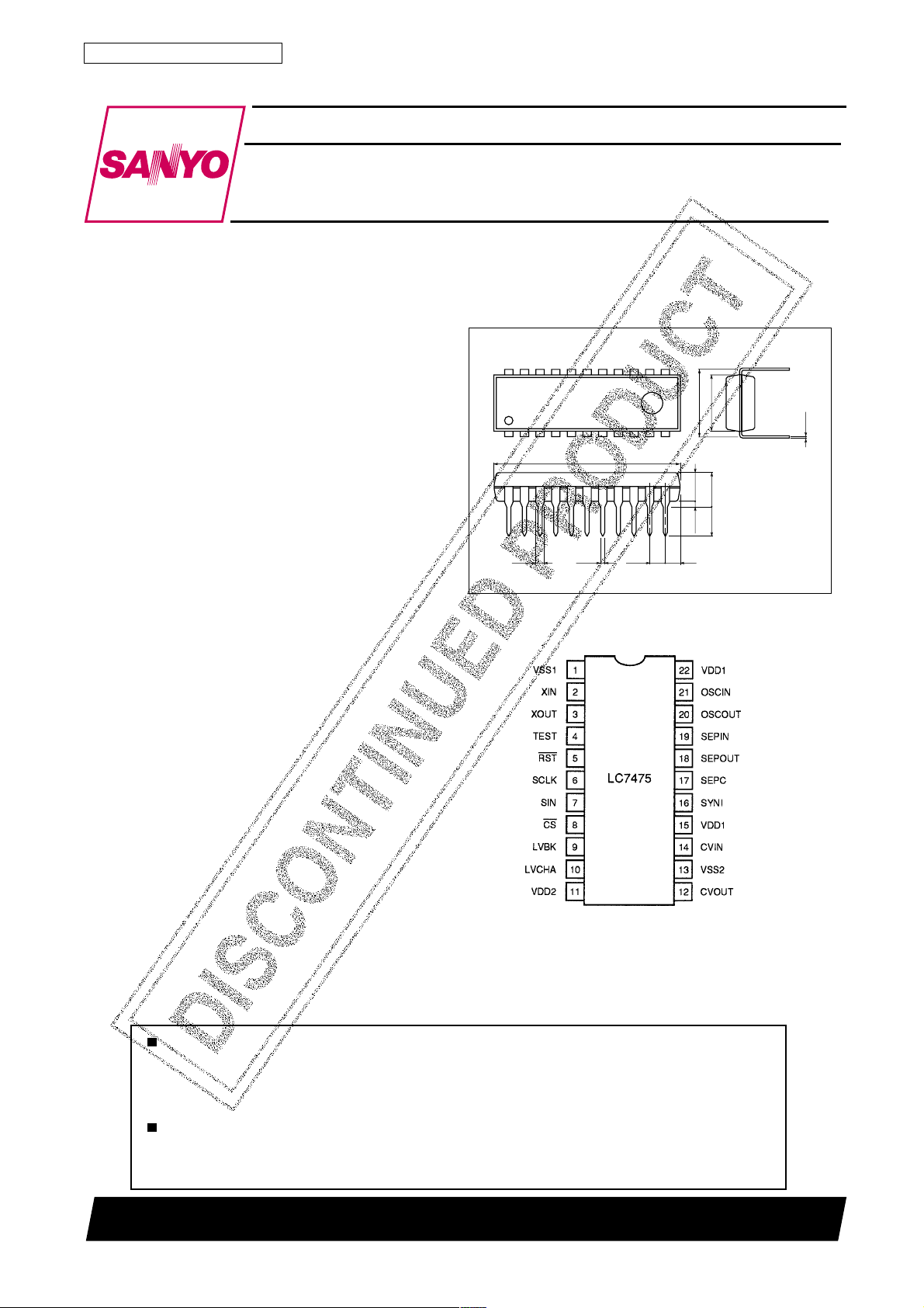
The LC7475 operates from a 5 V supply and is a v ailable in
22-pin shrink DIPs.
Features
• Complete text and graphics video overlay circuitry.
• 128 characters in internal ROM.
• 288 character display capability.
• 12 × 18 dot-matrix character resolution.
• Approximately 0.5 or 1 s period character flashing option.
• Selectable flashing duty cycles of 25, 50 or 75%.
• Internal or external synchronization.
• Serial data control.
• 5 V supply.
• 22-pin shrink DIP.
Package Dimensions
unit:mm
3059-DIP22S
[LC7475]
22 12
6.4
7.62
111
0.95 0.48
21.2
1.78
3.25
0.51min
1.7
3.9max
3.3
SANYO : DIP22S
Pin Assignment
0.25
Top view
71901TN (KT)/9021JN No.3885–1/12
Page 2
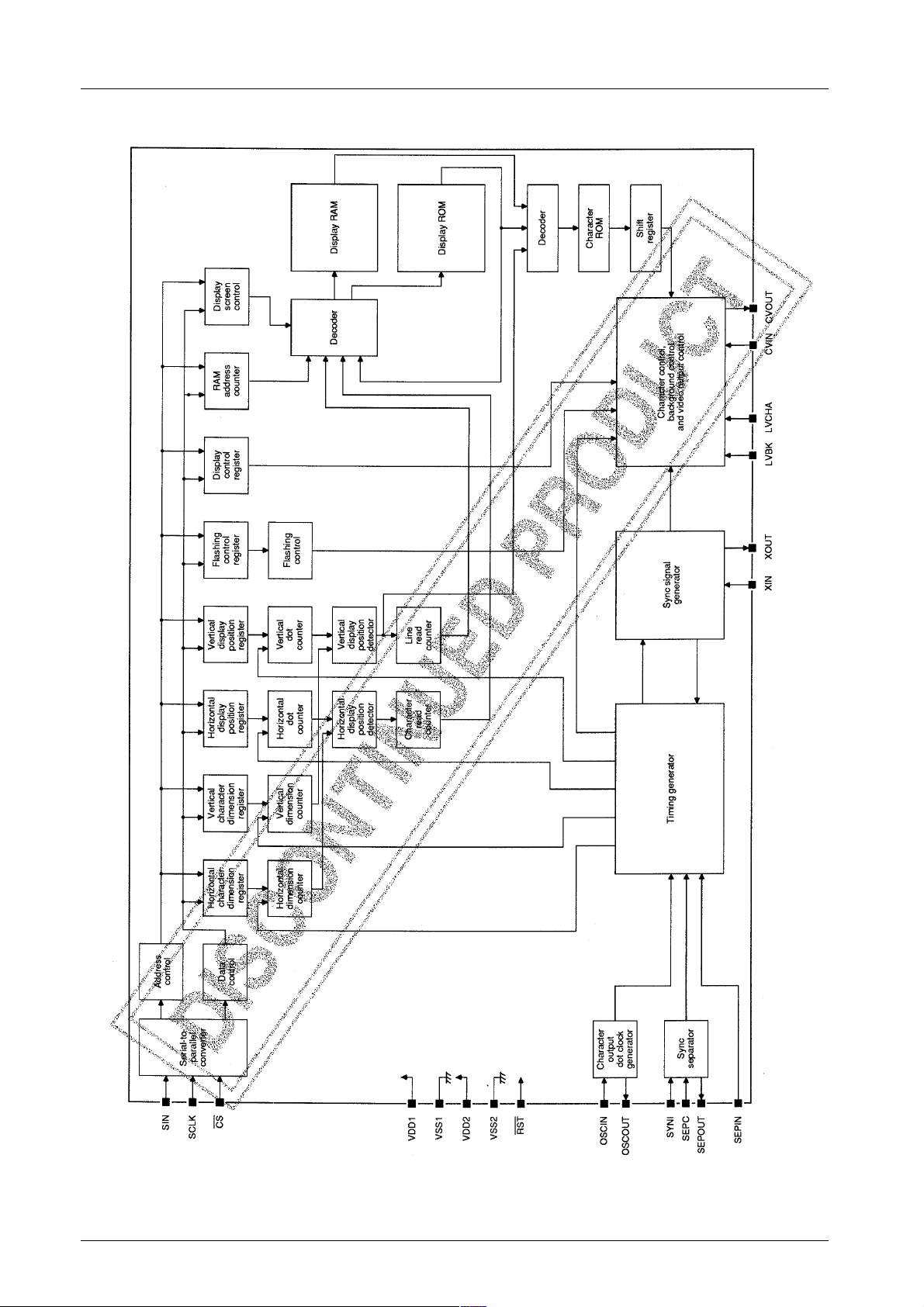
Block Diagram
LC7475
No.3885–2/12
Page 3
Pin Description
rebmuNemaNnoitpircseD
1V
2NIXtupnirotallicsolatsyrC
3TUOXtuptuorotallicsolatsyrC
4TSETtuptuotseT
5TSRtupniteseR
6KLCStupnikcolcatadlaireS
7NIStupniatadlaireS
8SCtupnitcelespihC
9KBVLtupnitnemtsujdalevel-gniknalB
01AHCVLtupnitnemtsujdalevel-retcaragC
11V
21TUOVCtuptuooedivetisopmoC
31V
41NIVCtupnioedivetisopmoC
51V
61INYStupnirotarapescnyS
71CPEStupnitnemtsujdarotarapescnyS
81TUOPEStuptuorotarapescnyS
91NIPEStupnicnyslacitreV
02TUOCSOtuptuorotallicsokcolctoD
12NICSOtupnirotallicsokcolctoD
22V
LC7475
1SS
2DD
2SS
1DD
1DD
dnuorgtiucriclatigiD
ylppustiucricgolanA
dnuorgtiucricgolanA
ylppuscigoL
ylppuscigoL
Specifications
Absolute Maximum Ratings
retemaraPlobmySsnoitidnoCsgnitaRtinU
egnaregatlovylppuSV
egnaregatlovtupnIV
egnaregatlovtuptuOV
noitapissidrewopelbawollAdPxam 52=aT(003 ˚ )CWm
erutarepmetgnitarepOrpoT 07+ot03–
erutarepmetegarotSgtsT 521+ot04–
Recommended Operating Conditions at Ta = 25˚C
retemaraPlobmySsnoitidnoCsgnitaRtinU
egatlovylppuscigoLV
egatlovylppusgolanAV
egnaregatlovylppuscigoLV
egnaregatlovylppusgolanAV
DD
I
O
1DD
2DD
1DD
2DD
V
V
V
Vot3.0–
0.7+
SS
SS
SS
SS
Vot3.0–
DD
Vot3.0–
DD
V72.1ot5.4
V
3.0+
V
3.0+
V
˚C
˚C
5V
5V
5.5ot5.4V
V
1DD
No.3885–3/12
Page 4
LC7475
Electrical Characteristics at T a = –30 to +70˚C, V
retemaraPlobmySsnoitidnoC
tnerrucylppuSI
egatlovtuptnilevel-wolTUOPESV
egatlovtupnilevel-wolKLCSdnaTSR,NIS,SCV
egatlovtupnilevel-hgihTUOPESV
tupnilevel-hgihKLCSdnaTSR,NIS,SC
egatlov
egatlovtupnioedivetisopmocINYSV
egatlovtupnioedivetisopmocNIVCV
level-hgihNIPESdnaKLCS,TSR,NIS,SC
tnerructupni
tnerructupnilevel-hgihNICSOI
ycneuqerftupnirotarenegcnySf
ycneuqerftupnikcolctoDf
tnerrucegakaelTUOVCI
Timing Characteristics at Ta = –30 to +75˚C, V
retemaraPlobmySsnoitidnoC
htdiwesluptupniKLCSt
htdiwesluptupnilevel-hgihSCt
emitputestupnielbaneatadSCt
emitputestupniatadNISt
emitdlohtupnielbaneatadSCt
emitdlohtupniatadNISt
emitetirwdrowtib-61t
emitetirwatadMARt
DD
V
1LI
2LI
V
1HI
V
2HI
1NI
2NI
I
1HI
2HI
1CSO
2CSO
L
DD1
)KLCS(W
)SC(W
)SC(US
)NIS(US
)SC(H
)NIS(H
drow
TW
= 5V, V
DD1
1DD
1DD
= 5±0.5V
= 5V, unless otherwise noted
DD2
sgnitaR
nimpytxam
I,V5.4=
Am1=0.1V
LO
I,V5.4=
Am1=5.3V
HO
VSS– 3.0V2.0
V8.0
1DD
0.25.2V
2V
–1Aµ
37.71zHM
5701zHM
sgnitaR
nimpytxam
002sn
1sµ
002sn
002sn
2sµ
002sn
01sµ
1sµ
V
1DD
02Am
1DD
3.0+
1Aµ
01Aµ
tinU
V
V
P-P
P-P
tinU
No.3885–4/12
Page 5

LC7475
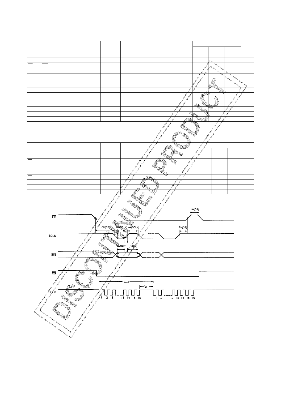
Input Timing
Data and address words are input in serial format on SIN. A 16-bit address word is input after the falling edge of CS
followed by 16-bit data words. The address is incremented automatically after each data word. The data input timing is
shown in figure 1.
Only the lower eight bits of the address word are significant. Only the lower eight bits of data words at addresses 000H
to 0AFH, the lower 11 bits of data words at addresses 0B0H to 0BBH, and the lower 12 bits of data words at addresses
0BCH to 0BFH are significant. All non-significant bits should be set to 0.
Figure 1. Input timing
RAM Memory Configuration
RAM memory is organized as 16-bit words as shown in table 1. Locations 000H to 0AFH are display RAM, locations
0B0H through to 0BBH are display line address registers, locations 0BCH to 0BDH are display control registers, location
0BEH is the video signal control register and location 0BFH is the general control register.
Table 1. Memory configuration
sserddA
FEDCBA9876543210
otH000
00000000 LFC6C5C4C3C2C1C
HFA0
×
H0B0 0000
H1B0 0000
H2B0 0000
H3B0 0000
H4B0 0000
H5B0 0000
H6B0 0000
H7B0 0000
H8B0 0000
H9B0 0000
HAB0 0000
HBB0 0000
HCB0 0000
HDB0 0000
HEB0 0000
HFB0 0000
ARDA9RDA8RDA7RDA6RDA5RDA4RDA3RDA2RDA1RDA0RDA
×
ARDA9RDA8RDA7RDA6RDA5RDA4RDA3RDA2RDA1RDA0RDA
×
ARDA9RDA8RDA7RDA6RDA5RDA4RDA3RDA2RDA1RDA0RDA
×
ARDA9RDA8RDA7RDA6RDA5RDA4RDA3RDA2RDA1RDA0RDA
×
ARDA9RDA8RDA7RDA6RDA5RDA4RDA3RDA2RDA1RDA0RDA
×
ARDA9RDA8RDA7RDA6RDA5RDA4RDA3RDA2RDA1RDA0RDA
×
ARDA9RDA8RDA7RDA6RDA5RDA4RDA3RDA2RDA1RDA0RDA
×
ARDA9RDA8RDA7RDA6RDA5RDA4RDA3RDA2RDA1RDA0RDA
×
ARDA9RDA8RDA7RDA6RDA5RDA4RDA3RDA2RDA1RDA0RDA
×
ARDA9RDA8RDA7RDA6RDA5RDA4RDA3RDA2RDA1RDA0RDA
×
ARDA9RDA8RDA7RDA6RDA5RDA4RDA3RDA2RDA1RDA0RDA
×
ARDA9RDA8RDA7RDA6RDA5RDA4RDA3RDA2RDA1RDA0RDA
13ZSH03ZSH12ZSH02ZSH11ZSH01ZSH
13ZSV03ZSV12ZSV02ZSV11ZSV01ZSV
/TNI
NON
TST
DOM
f2CS/
×
f4
CS
××
CSO
PTS
1KLB0KLB
stnetnocyromeM
0
MORenilni
MORenilni
MORenilni
MORenilni
MORenilni
MORenilni
MORenilni
MORenilni
MORenilni
MORenilni
MORenilni
MORenilni
5PH4PH3PH2PH1PH0PH
5PV4PV3PV2PV1PV0PV
PSD
NO
SYS
×
TSR
×
2LF1LF0LFTXE
××
2HP1HP0HP
BC
FFO
LOCB
noisnemied
noisnemied
noitpircseD
retcarahctib-7htiwMARyalpsiD
tibelbanegnihsalfdnaedoc
1enilforetcarahctsriffosserddA
2enilforetcarahctsriffosserddA
3enilforetcarahctsriffosserddA
4enilforetcarahctsriffosserddA
5enilforetcarahctsriffosserddA
6enilforetcarahctsriffosserddA
7enilforetcarahctsriffosserddA
8enilforetcarahctsriffosserddA
9enilforetcarahctsriffosserddA
dnanoitisopretcarahclatnoziroH
dnanoitisopretcarahclacvitreV
yalpsid,esahplangisoediV
dnalortnocrotallicso,gniknalb
noitcelestesermetsys
noitcelesedomtset
dna,gnihsalf,gniknalbretcarahC
01enilforetcarahctsriffosserddA
11enilforetcarahctsriffosserddA
21enilforetcarahctsriffosserddA
Note
× = don’t care
No.3885–5/12
Page 6

LC7475
Horizontal Display Control Register
The function of each bit in the horizontal display control register is shown in table 2. Note that all bits can be reset to 0
by a reset pulse on RST.
Table 2. Horizontal display control register (0BCH)
tibataDemaN noitcnuF
00PH
11PH
22PH
33PH
44PH
55PH
601ZSH
711ZSH
802ZSH
912ZSH
A03ZSH
B13ZSH
C – noitcnufoN
Terehw
C
Table 3. Horizontal dimension of characters in line 1
11ZSH01ZSHnoisnemidlatnoziroH
00 T1Ctod/
01 T2Ctod/
10 T3Ctod/
11 T4Ctod/
T4foselpitlumnistnemercniSHtahtetoN.rotallicsokcolctodehtfodoirepehtsi
C
3elbatninwohssa1enilnisretcarahcfonoisnemidlatnozirohehtstceleS
4elbatninwohssa2enilnisretcarahcfonoisnemidlatnozirohehtstceleS
5elbatninwohssa21ot3senilnisretcarahcfonoisnemidlatnozirohehtstceleS
noitauqegniwollofehtybnevigsa,SH,neercsehtnoyalpsidethfonoitisoptratslatnozirohehtstceleS
Table 4. Horizontal dimension of characters in line 2
12ZSH02ZSHnoisnemidlatnoziroH
00 T1Ctod/
01 T2Ctod/
10 T3Ctod/
11 T4Ctod/
Table 5. Horizontal dimension of characters in lines 3 to 12
13ZSH03ZSHnoisnemidlatnoziroH
00 T1Ctod/
01 T2Ctod/
10 T3Ctod/
11 T4Ctod/
Vertical Display Control Register
The function of each bit in the vertical display control register is shown in table 6. Note that all bits can be reset to 0
by a reset pulse on RST.
Table 6. Vertical display control register (0BDH)
tibataDemaN noitcnuF
00PV
11PV
22PV
33PV
44PV
55PV
601ZSV
711ZSV
802ZSV
912ZSV
A03ZSV
B13ZSV
C – noitcnufoN
7elbatninwohssa1enilnisretcarahcfonoisnemidlacitrevehtstceleS
8elbatninwohssa2enilnisretcarahcfonoisnemidlacitrevehtstceleS
9elbatninwohssa21ot3senilnisretcarahcfonoisnemidlacitrevehtstceleS
noitauqegniwollofehtybnevigsa,SV,neercsehtnoyalpsidethfonoitisoptratslacitrevehtstceleS
46enilot0enilmorfsenil4foselpitlumnistnemercniSVtahtetoN.htdiweslupcnyslatnozirohehtsiHerehw
No.3885–6/12
Page 7

LC7475
Table 7. Vertical dimension of characters in line 1
11ZSH01ZSHnoisnemidlacitreV
00 T1Ctod/
01 T2Ctod/
10 T3Ctod/
11 T4Ctod/
Table 8. Vertical dimension of characters in line 2
12ZSH02ZSHnoisnemidlacitreV
00 T1Ctod/
01 T2Ctod/
10 T3Ctod/
11 T4Ctod/
Table 9. Vertical dimension of characters in lines 3 to 12
13ZSV03ZSVnoisnemidlacitreV
00 T1Ctod/
01 T2Ctod/
10 T3Ctod/
11 T4Ctod/
The relationships between the vertical sync and horizontal sync pulses and between the horizontal and vertical display
start positions are shown in figure 2.
Figure 2. Vertical and horizontal sync pulses
Video Signal Control Register
The function of each bit in the video signal control register is shown in table 10. Note that all bits can be reset to 0 by
a reset pluse on RST.
Table 10. Video signal control register (0BEH)
tibataDemaN noitcnuF
00HP
3erugifdna11elbatninwohssatsrubrolocehtni,rolocdnuorgkcabehtecnehdna,esahpehtstceleS11HP
22HP
3 – noitcnufoN
4 – noitcnufoN
5TSRSYS WOLseogSCnehwsruccooslatesermetsysatahtetoN.1nehwFFOyalpsidehtsnrutdnasretsigerllasteseR
6 – noitcnufoN
7NOPSD1nehw,NOdna,0nehwFFOyalpsidretcarahcstceleS
8PTSCSO
9f2CSf4/
A – noitcnufoN
BNON/TNI 1nehw,yalpsiddecalretni-non,dleif/senil313dna,0nehwyalpsiddecalretni,dleif/senil5.213stceleS
C – noitcnufoN
CS
FFOsiyalpsidretcarahcehtnehwylnoevitceffesinoitazinorhcnyslanretxe
f2foycneuqerfkcolcastceleS
CS
f4dna,0nehw
1nehw,
CS
tahtetoN.0nehw,sihtstneverpdna,1nehwFFOdenrutebotrotallicsoCLdnarotallicsolatsyrcehtswollA
No.3885–7/12
Page 8

Table 11. Phase selection
2HP1HP0HPesahProloC
000 ±π 2/nayC
001 0 wolleY
010 ±π 2/deR
011 ±π eulB
100 3± π 4/nayc-eulB
101 ±π 4/neerG
110 ±π 4/wolley-deR
111 3± π 4/atnegaM
LC7475
Figure 3. Background color-phase vector diagram
General Control Register
The function of each bit in the general control register is shown in table 12. Note that all bits can be reset to 0 by a
reset pulse on RST.
Table 12. General control register
tibataDemaN noitcnuF
0LOCB 1nehw,FF0dna,)ylnonoitazinorhcnyslanretnirofdilav(0nehwNOrolocdnuorgkcabstceleS
1FFOBC1siLOCBdna1nehwro,0nehwtsrubrolocehtstceleS
2TXE 1nehw,lanretnidna,0nehwnoitazinorhcnyslacitrevdnalatnozirohlanretxestceleS
30LF
41LF
52LF 1nehw,s5.0yletamixorppafodna,0nehws1yletamixorppafodoirepgnihsalfastceleS
6 – noitcnufoN
70KLB
81KLB
9 – noitcnufoN
A – noitcnufoN
BDOMTST
C – noitcnufoN
noitarepo
31elbatninwohssaelcycytudgnihsalfyalpsidehtstceleS
41elbatninwohssayalpsidehtfoaeragniknalbehtstceleS
Table 13. Flashing duty cycle selection
1LF0LFelcycytuD
00 FFOgnihsalF
01 %52
10 %05
11 %57
lamrongniruddetcelesebtondluohsedomtsettahtetoN.1nehw,edomtsetdna,0nehwnoitarepolamronstceleS
Table 14. Blanking area selection
1KLB0KLBaeragniknalB
00 FFOgniknalB
01 ezisretcarahC
10 ezisemarF
11 aeralatoT
No.3885–8/12
Page 9

LC7475
Line ROM Configuration
The line ROM is configured as 1,536 words from address 000H to 5FFH as shown in table 15. Each word comprises a
16-bit address code and a single control bit. When the control bit is 0, the 7-bit character code is significant and is
used to address the character ROM, and when 1, the 7-bit character code in ROM is ignored and the character code is
read from display RAM. The display RAM address is incremented automatically by one each time a character code is
read from RAM. Note that your local SANYO representative can offer advice on how to specify character ROM.
Table 15. Line ROM configuration
sserddA
FEDCBA9876543210
H000 00000000
H710 00000000
H810 00000000
HFF5 00000000
The function of each significant bit in a line ROM word is shown in table 16.
Table 16. Line ROM word data
tibataDemaN noitpircseD
00RDA
11RDA
22RDA
33RDA
44RDA
55RDA
66RDA
7MAR/MOR
stiblortnoclangisoediV
/MOR
6RDA5RDA4RDA3RDA2RDA1RDA0RDA
MAR
ot
/MOR
6RDA5RDA4RDA3RDA2RDA1RDA0RDA
MAR
/MOR
6RDA5RDA4RDA3RDA2RDA1RDA0RDA
MAR
ot
/MOR
6RDA5RDA4RDA3RDA2RDA1RDA0RDA
MAR
gnisserddaMORtceridstceleS
MARmorfgnisserddaMORtceridnistceleS
1enilfo
46enilfo
1si7tibnehw0ottesebdluohs6RDAot0RDA.sserddaMORretcarahcehtseificepS
noitpircseD
1enilforetcarahctsriffosserddA
retcarahchtruof-ytnewtfosserddA
2enilforetcarahctsriffosserddA
retcarahchtruof-ytnewtfosserddA
The line addresses in line ROM are shown in table 17.
Table 17. Line ROM addresses
eniL)xeh(sserddAeniL)xeh(sserddAeniL)xeh(sserddAeniL)xeh(sserddA
100710813300394084
281818914381305894
303910B153033150B4
484028C163843258C4
506120E173063350E4
687228F183873458F4
709320129309355015
88A42822048A365825
90C52042140C375045
018D62852248D385855
110F72072340F395075
21801828824480406885
31021920A254024160A5
41831038B264834268B5
51051130D274054360D5
61861238E284864468E5
No.3885–9/12
Page 10

LC7475
Screen Configuration
The character screen display is configured as 12 lines × 24 characters, making a maximum number of 288 characters
when the smallest character size is used. The number of characters that can be displayed reduces as character size is
increased. The character screen configuration is shown in table 18.
Table 18. Screen configuration
eniL
1001020304050607080900111213141516171819102122232
2425262728292031323334353637383930414243444546474
3849405152535455565758595061626364656667686960717
4273747576777879708182838485868788898091929394959
569798999001101201301401501601701801901011111211311411511611711811911
6021121221321421521621721821921031131231331431531631731831931041141241341
7441541641741841941051151251351451551651751851951061161261361461561661761
8861961071171271371471571671771871971081181281381481581681781881981091191
9291391491591691791891991002102202302402502602702802902012112212312412512
01612712812912022122222322422522622722822922032132232332432532632732832932
11042142242342442542642742842942052152252352452552652752852952062162262362
21462562662762862962072172272372472572672772872972082182282382482582682782
The start address for each of the twelve display lines is specified in the display line address registers in RAM. An
example arrangement of ROM and RAM addresses is shown in table 19. Note how both the RAM and ROM addresses
increment.
Table 19. Example ROM and RAM configuration
eniL
123456789 011121314151617181910212223242
MOR
MOR
MOR
MOR
MOR
MOR
MOR
MOR
MOR
MOR
MOR
1
00
10
20
30
40
50
60
70
80
MOR
MAR
MAR
MAR
MAR
MOR
MOR
2
81
60
70
80
90
MOR
MAR
MAR
3
03
01
MOR
4
5
6
7
8
9
01
11
21
MOR
84
94
MOR
MAR
06
92
MOR
MAR
87
73
MAR
MAR
94
A4
MAR
MAR
55
65
MOR
MOR
0C
1C
MOR
MOR
8D
9D
MOR
MOR
0F
1F
MAR
MAR
18
28
MAR
11
21
MOR
MOR
A4
B4
MAR
MAR
A2
B2
MAR
MAR
83
93
MAR
MAR
B4
C4
MAR
MAR
75
85
MOR
MOR
2C
3C
MOR
MOR
AD
BD
MOR
MOR
2F
3F
MAR
MAR
38
48
D1
MAR
MAR
31
41
MOR
MAR
C4
F1
MAR
MAR
C2
D2
MAR
MAR
A3
B3
MAR
MAR
D4
E4
MAR
MAR
95
A5
MOR
MOR
4C
5C
MOR
MAR
CD
D6
MOR
MOR
4F
5F
MAR
MAR
58
68
MOR
E1
F1
MOR
MOR
63
73
MAR
MAR
02
12
MAR
MAR
E2
F2
MAR
MAR
C3
D3
MAR
MAR
F4
05
MAR
MAR
B5
C5
MOR
MOR
6C
7C
MAR
MAR
E6
F6
MOR
MOR
6F
7F
MAR
MAR
78
88
90
MOR
MOR
02
12
MOR
MOR
83
93
MAR
MOR
22
15
MAR
MOR
03
96
MOR
MAR
08
E3
MAR
MAR
15
25
MAR
MAR
D5
E5
MOR
MOR
8C
9C
MAR
MAR
07
17
MOR
MOR
8F
9F
MAR
MAR
98
A8
MOR
A0
B0
MAR
MAR
A0
B0
MAR
MAR
51
61
MAR
MAR
32
42
MAR
MAR
13
23
MAR
MAR
F3
04
MAR
MAR
35
45
MAR
MAR
F5
06
MOR
MOR
AC
BC
MAR
MAR
27
37
MOR
MOR
AF
BF
MAR
MAR
B8
C8
rebmunretcarahC
)xeh(noitarugifnocMORdnaMARretcarahC
MOR
MOR
MOR
MOR
MAR
MAR
MAR
MAR
MAR
MAR
C0
D0
E0
F0
00
10
20
30
MAR
MAR
MAR
MAR
MOR
MOR
C0
D0
E0
F0
MAR
MAR
71
MOR
45
MOR
C6
MAR
14
MOR
C9
MOR
4B
MAR
16
MAR
47
MOR
CF
MAR
D8
MAR
81
91
MAR
MAR
52
62
MAR
MAR
33
43
MOR
MAR
58
24
MOR
MOR
D9
E9
MOR
MOR
5B
6B
MAR
MAR
26
36
MAR
MAR
57
67
MOR
MOR
DF
EF
MAR
MAR
E8
F8
82
MAR
MAR
A1
B1
MOR
MAR
75
72
MOR
MAR
F6
53
MAR
MAR
34
44
MOR
MOR
F9
0A
MOR
MOR
7B
8B
MAR
MAR
46
56
MAR
MAR
77
87
MAR
MAR
B7
C7
MAR
MAR
09
19
MOR
92
A2
MAR
MAR
C1
D1
MAR
MOR
82
A5
MAR
MOR
63
27
MAR
MAR
54
64
MOR
MOR
1A
2A
MOR
MOR
9B
AB
MAR
MAR
66
76
MAR
MAR
97
A7
MOR
MAR
101
D7
MAR
MAR
29
39
40
MOR
MOR
B2
C2
MAR
MOR
E1
44
MOR
MOR
B5
C5
MOR
MOR
37
47
MOR
MAR
B8
74
MOR
MOR
3A
4A
MOR
MOR
BB
CB
MAR
MAR
86
96
MOR
MOR
BE
CE
MAR
MOR
E7
401
MAR
MAR
49
59
MOR
50
61
MOR
MOR
D2
E2
MOR
MOR
54
64
MOR
MOR
D5
E5
MOR
MOR
57
67
MAR
MOR
84
E8
MOR
MOR
5A
6A
MOR
MOR
DB
EB
MAR
MAR
A6
B6
MOR
MOR
DE
EE
MAR
MAR
F7
08
MAR
MAR
69
79
MOR
71
MOR
F2
MOR
74
MOR
F5
MOR
77
MOR
F8
MOR
7A
MOR
FB
MAR
C6
MOR
FE
MOR
701
MOR
F11
No.3885–10/12
Page 11

LC7475
Composite Video Output
The character and background images are superimposed onto the composite video signal, which is shown in figure 4.
Figure 4. Composite video output waveform
The relative carrier amplitude and the corresponding DC voltage output amplitude are shown in table 20.
Table 20. Relative amplitude and DC output amplitude
)ERI(edutilpmareirracevitaleR )V(edutilpmaegatlovtuptuO
0.001 08.2
1.58 95.2
8.06 52.2
5.12 07.1
7.5 84.1
0 04.1
5.12– 01.1
0.34– 08.0
No.3885–11/12
Page 12

LC7475
Specifications of any and all SANYO products described or contained herein stipulate the performance,
characteristics, and functions of the described products in the independent state, and are not guarantees
of the performance, characteristics, and functions of the described products as mounted in the customer's
products or equipment. To verify symptoms and states that cannot be evaluated in an independent device,
the customer should always evaluate and test devices mounted in the customer's products or equipment.
SANYO Electric Co., Ltd. strives to supply high-quality high-reliability products. However, any and all
semiconductor products fail with some probability. It is possible that these probabilistic failures could
give rise to accidents or events that could endanger human lives, that could give rise to smoke or fire,
or that could cause damage to other property. When designing equipment, adopt safety measures so
that these kinds of accidents or events cannot occur. Such measures include but are not limited to protective
circuits and error prevention circuits for safe design, redundant design, and structural design.
In the event that any or all SANYO products(including technical data,services) described or
contained herein are controlled under any of applicable local export control laws and regulations,
such products must not be exported without obtaining the export license from the authorities
concerned in accordance with the above law.
No part of this publication may be reproduced or transmitted in any form or by any means, electronic or
mechanical, including photocopying and recording, or any information storage or retrieval system,
or otherwise, without the prior written permission of SANYO Electric Co. , Ltd.
Any and all information described or contained herein are subject to change without notice due to
product/technology improvement, etc. When designing equipment, refer to the "Delivery Specification"
for the SANYO product that you intend to use.
Information (including circuit diagrams and circuit parameters) herein is for example only ; it is not
guaranteed for volume production. SANYO believes information herein is accurate and reliable, but
no guarantees are made or implied regarding its use or any infringements of intellectual property rights
or other rights of third parties.
This catalog provides information as of July, 2001. Specifications and information herein are subject to
change without notice.
PS No.3885–12/12
 Loading...