

Page 1
Ordering number : ENN*7191
42602RM (OT) No. 7191-1/50
Overview
The LC74735W is an on-screen display CMOS IC that
displays characters and patterns on a TV screen.
For QVGA display, the LC74735W supports the use of
both a 12×18 dot character font and a 12×18 dot graphics
font with 16 colors with a total of 512 characters and
glyphs.
For WVGA display, the LC74735W supports the use of
both a 24×32 dot character font and a 12×16 dot graphics
font with 16 colors with a total of 512 characters and
glyphs.
The LC74735W can also implement extremely varied
displays by the use of an external ROM.
The LC74735W supports both QVGA (480×234) and
WVGA (800×480).
Features
• Screen structure
— Main:
QVGA mode: 40 characters × 13 lines (up to 520
characters) on a QVGA panel
WVGA mode: 33 characters × 15 lines (up to 495
characters) on a WVGA panel
— Wallpaper display screen: Permanent repetition of a
2×2 (horizontal × vertical) character pattern
• Character structure
— QVGA mode:
12 dots (horizontal) × 18 dots (vertical): Character
display
12 dots (horizontal) × 18 dots (vertical): Graphic
glyph display
— WVGA mode:
24 dots (horizontal) × 32 dots (vertical): Character
display
12 dots (horizontal) × 16 dots (vertical): Graphic
glyph display (1 pixel: 2x2 dots)
— Character display clock: About 9 MHz — QVGA
with an LC oscillator
33.2 MHz (maximum: 40 MHz) WVGA with an
external clock signal input
*: The ROM image is known when QVGA or WVGA
mode is specified.
• Number of characters: 512 (internal)
Up to 2048 characters when an external 16-bit 4M ROM
is used.
• Character sizes: Four horizontal sizes (1×, 2×, 3×, and
4×)
Four vertical sizes (1×, 2×, 3×, and 4×)
The character size is specified in line units.
• Display start positions: 512 positions in the horizontal
direction and 256 positions in the vertical direction.
QVGA mode - WVGA mode
Setting units: Horizontal: 1 dot - 2 dots (In screen units)
Vertical: 1 dot - 2 dots (In screen units)
• Display functions
— Blinking specification (In character units)
Period: 1/64, 1/32, and 1/16 of the vertical sync
signal (In screen units)
Duty: Fixed at 50%
— Box (raised or recessed) display
Raised/depressed specification (In character units)
Left: Off/on specification (In character units)
Right: Off/on specification (In character units)
Top: Off/on specification (In character units)
Bottom: Off/on specification (In character units)
— Border specification (In line units): Only valid with
glyphs from the character font.
Preliminary
LC74735W
SANYO Electric Co.,Ltd. Semiconductor Company
TOKYO OFFICE Tokyo Bldg., 1-10, 1 Chome, Ueno, Taito-ku, TOKYO, 110-8534 JAPAN
On-Screen Display Controller
CMOS IC
Any and all SANYO products described or contained herein do not have specifications that can handle
applications that require extremely high levels of reliability, such as life-support systems, aircraft’s
control systems, or other applications whose failure can be reasonably expected to result in serious
physical and/or material damage. Consult with your SANYO representative nearest you before using
any SANYO products described or contained herein in such applications.
SANYO assumes no responsibility for equipment failures that result from using products at values that
exceed, even momentarily, rated values (such as maximum ratings, operating condition ranges, or other
parameters) listed in products specifications of any and all SANYO products described or contained
herein.
Page 2
• Color specification
Character
— Character color (In character units): 1 of 16 colors
can be specified.
— Character background color (In character units): 1 of
16 colors can be specified.
— Border color (In line units): 1 of 16 colors can be
specified.
• Graphic
— 16 types can be specified by ROM data
• Box color (line units) : 1/16 cdors
• Background color (screen units) : 1/16 colors
• Color table (palette)
— Sixteen colors can be selected from a set of 512
colors (One of which is specified to be transparent.)
— Number of color tables: 2. This allows up to 32
colors to be displayed at the same time.
• Wallpaper screen (Graphics glyphs only)
Wallpaper display: Repeated display under the main
screen (2 characters horizontally by 2 characters
vertically).
Sprite character display: Displayed above the main
screen (2 characters horizontally by 2 characters
vertically)
• Output
— QVGA
Analog RGB output
BLK (OSD display period signal)
— WVGA
Digital RGB output (3 bits per color)
BLK (OSD display period signal)
• Package: SQFP80
• Voltage: 3.3 V
Package Dimensions
unit: mm
3220-SQFP80
No. 7191-2/50
LC74735W
14.0
12.0
1.25 1.25
0.5
14.0
12.0
1.25
1.25
0.5
1 20
21
40
41
60
61
80
0.1
0.5
1.6max
1.4
0.5
0.2
0.135
SANYO: SQFP80
[LC74735W]
Page 3

Pin Assignment
No. 7191-3/50
LC74735W
1
2
3
4
5
6
7
8
9
10
11
12
13
14
15
16
17
18
19
20
60
59
58
57
56
55
54
53
52
51
50
49
48
47
46
45
44
43
42
41
A16
A17
CE
OE
VDD3
VSS3
D0
D1
D2
D3
D4
D5
D6
D7
VDD1
VSS1
D8
D9
D10
D11
VSS1
OSCin
OSCout
CTRL1
SCLK
SIN
CS
VDD1
VSYNC
VBLK
HSYNC
HBLK
TEST1
TEST2
RST
VSS1
VDD1
CLKOUT
VSS1
VDD1
VSS2
RREF
CVREF
COMP
BOUT
GOUT
ROUT
OUTR
VDD2
VSS1
BLK
BD0
BD1
BD2
GD0
GD1
GD2
RD0
RD1
RD2
80
79
78
77 76 75 74 73 72 71 70 69 68 67 66
65
64 63 62 61
21
22
23
24 25 26 27 28 29 30 31 32 33 34 35
36
37 38 39 40
VDD3
VSS3A0A1
A2
A3
A4
A5
A6
A7
VDD3
VSS3A8A9
A10
A11
A12
A13
A14
A15
Page 4
No. 7191-4/50
LC74735W
Pin Functions
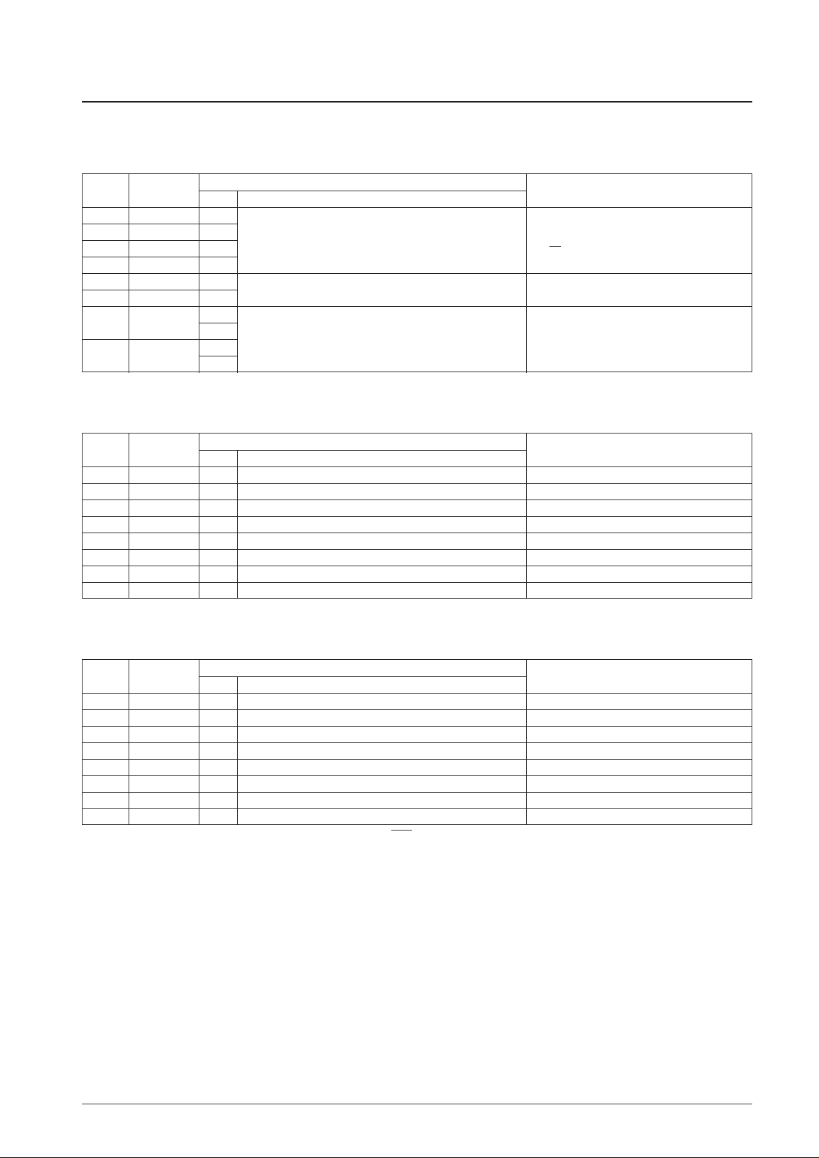
Pin No. Symbol Type Functional description
1 V
SS
1 Ground Digital system ground
2 OSCin
LC oscillator
Connections for the character output dot clock generator oscillator coil and capacitor.
3 OSCout
May also be used for external clock input.
4 CTRL1 OSCin oscillator input control
Switches between external clock input mode and LC oscillator mode.
Low: LC oscillator, high: external clock input MORE+
5 SCLK Clock input
Clock input for the serial data input system
MORE+ (This input has hysteresis characteristics.)
6 SIN Data input
Serial data input
MORE+ (This input has hysteresis characteristics.)
7 CS Enable input
Enable input for the serial data input system. Serial data input is enabled when this pin is low.
MORE+ (This input has hysteresis characteristics.)
8 VDD1 Power supply (+3.3 V) Digital system power supply: +3.3 V
9 VSYNC Vertical sync signal input
Vertical sync signal input
MORE+ (This input has hysteresis characteristics.)
10 VBLK Vertical blanking signal input
Vertical blanking signal input
MORE+ (This input has hysteresis characteristics.)
11 HSYNC Horizontal sync signal input
Horizontal sync signal input
MORE+ (This input has hysteresis characteristics.)
12 HBLK
Horizontal blanking signal input
Horizontal blanking signal input
MORE+ (This input has hysteresis characteristics.)
13 TEST1 Test mode control 1
Test mode control 1
Low: normal operation, high: test mode MORE+
14 TEST2 Test mode control 2
Test mode control 2
Low: normal operation, high: test mode (scan mode) MORE+
15 RST Reset input
System reset input
MORE+ (This input has hysteresis characteristics.)
16 VSS1 Ground Digital system ground
17 VDD1 Power supply (+3.3 V) Digital system power supply: +3.3 V
18 CLKOUT Clock output Clock output
19 VSS1 Ground Digital system ground
20 VDD1 Power supply (+3.3 V) Digital system power supply: +3.3 V
21 RD2 Rout output: bit 2
Rout output
22 RD1 Rout output: bit 1
This is a 3-bit digital output with values from 000 to 111.
23 RD0 Rout output: bit 0
24 GD2 Gout output: bit 2
Gout output
25 GD1 Gout output: bit 1
This is a 3-bit digital output with values from 000 to 111.
26 GD0 Gout output: bit 0
27 BD2 Bout output: bit 2
Bout output
28 BD1 Bout output: bit 1
This is a 3-bit digital output with values from 000 to 111.
29 BD0 Bout output: bit 0
30 BLK Blanking signal output This signal indicates the OSD display period.
31 VSS1 Ground Digital system ground
32 VDD2 Power supply (+3.3 V) Analog system power supply: +3.3 V
33 Outr outr output: analog Output. Connect a resistor Ro (67 Ω) to this pin.
34 Rout Rout output: analog D/A converter (3 bits) output. Connect a resistor Ro (200 Ω) to this pin.
35 Gout Gout output: analog D/A converter (3 bits) output. Connect a resistor Ro (200 Ω) to this pin.
36 Bout Bout output: analog D/A converter (3 bits) output. Connect a resistor Ro (200 Ω) to this pin.
37 CCOMP
Phase correction capacitor connection
Capacitor connection: 1.5 µF
38 CVREF Reference voltage output Capacitor connection: 0.1 µF
39 RREF
Reference resistor connection
Resistor connection: ro, 1540 Ω
40 VSS2 Ground D/A converter ground
Continued on next page.
Page 5
No. 7191-5/50
LC74735W
Continued from preceding page.
Pin No. Symbol Type Functional description
41 D11 Data input 11 ROM data input 11. MORE+
42 D10 Data input 10 ROM data input 10. MORE+
43 D9 Data input 9 ROM data input 9. MORE+
44 D8 Data input 8 ROM data input 8. MORE+
45 VSS1 Ground Digital system ground
46 VDD1 Power supply (+3.3 V) Digital system power supply: +3.3 V
47 D7 Data input 7 ROM data input 7. MORE+
48 D6 Data input 6 ROM data input 6. MORE+
49 D5 Data input 5 ROM data input 5. MORE+
50 D4 Data input 4 ROM data input 4. MORE+
51 D3 Data input 3 ROM data input 3. MORE+
52 D2 Data input 2 ROM data input 2. MORE+
53 D1 Data input 1 ROM data input 1. MORE+
54 D0 Data input 0 ROM data input 0. MORE+
55 VSS3 Ground External ROM output system ground
56 VDD3
Power supply (+3.3 or +5.5 V)
External ROM output system power supply
57 OE Output enable ROM output enable output. This is an active low output.
58 CE Chip enable ROM chip enable output. This is an active low output.
59 A17 Address output 17 ROM address output 17
60 A16 Address output 16 ROM address output 16
61 A15 Address output 15 ROM address output 15
62 A14 Address output 14 ROM address output 14
63 A13 Address output 13 ROM address output 13
64 A12 Address output 12 ROM address output 12
65 A11 Address output 11 ROM address output 11
66 A10 Address output 10 ROM address output 10
67 A9 Address output 9 ROM address output 9
68 A8 Address output 8 ROM address output 8
69 VSS3 Ground External ROM output system ground
70 VDD3
Power supply (+3.3 or +5.5 V)
External ROM output system power supply
71 A7 Address output 7 ROM address output 7
72 A6 Address output 6 ROM address output 6
73 A5 Address output 5 ROM address output 5
74 A4 Address output 4 ROM address output 4
75 A3 Address output 3 ROM address output 3
76 A2 Address output 2 ROM address output 2
77 A1 Address output 1 ROM address output 1
78 A0 Address output 0 ROM address output 0
79 VSS3 Ground External ROM output system ground
80 VDD3
Power supply (+3.3 or +5.5 V)
External ROM output system power supply
Page 6
No. 7191-6/50
LC74735W
Specifications
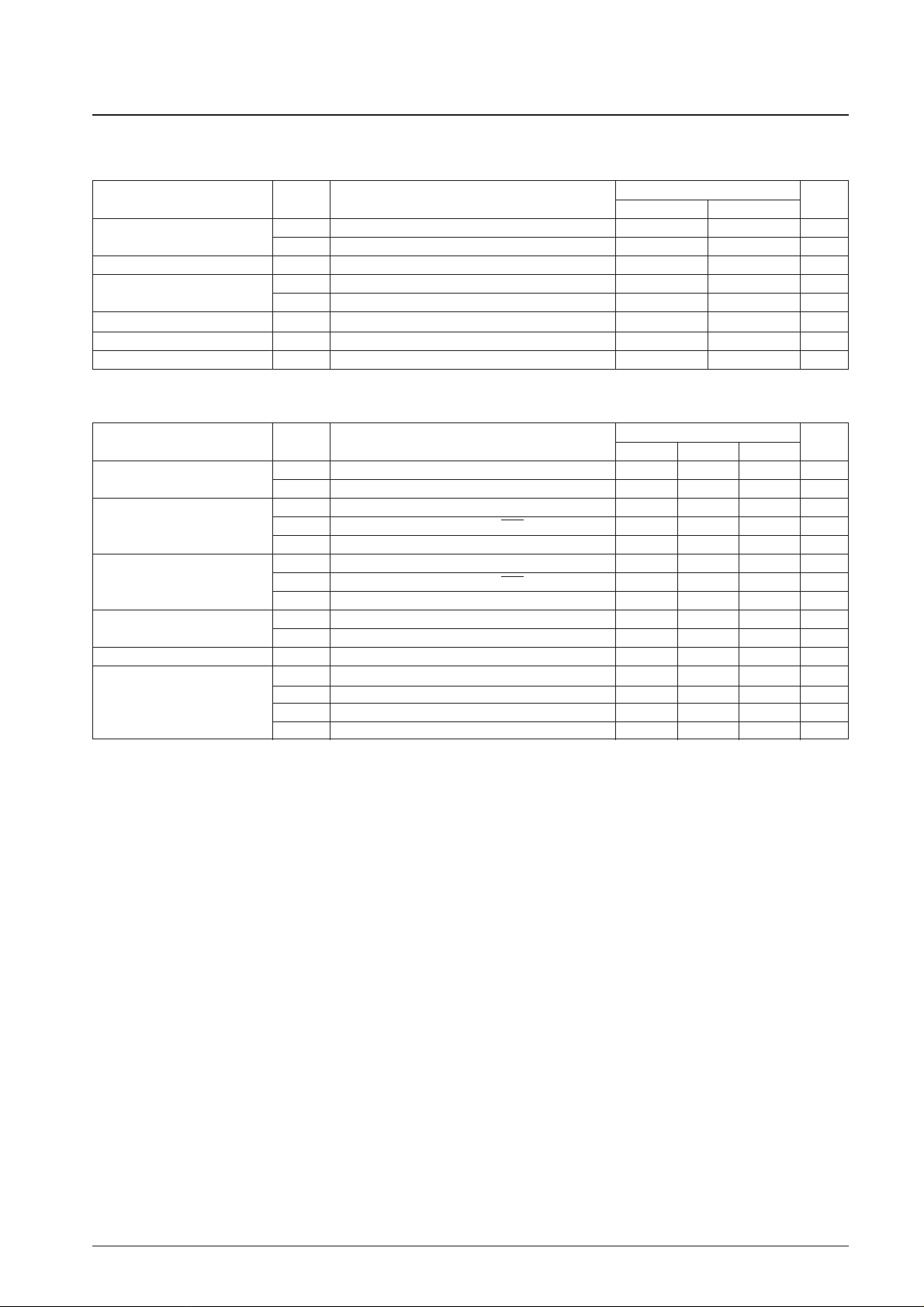
Maximum Ratings
Parameter Symbol Conditions
Ratings
Unit
min max
Supply voltage
V
DD
1 VDD1, VDD2 VSS– 0.3 VSS+ 4.6 V
V
DD
3 VDD3 (A0 to A17, CE, OE) VSS– 0.3 VSS+ 6.0 V
Input voltage V
IN
All input pins VSS– 0.3 VDD1 + 0.3 V
Output voltage
V
OUT
1 RD2:0, GD2:0, BD2:0, and BLK outputs VSS– 0.3 VDD1 + 0.3 V
V
OUT
2 A0 to A17, OE, CE outputs VSS– 0.3 VDD1 + 0.3 V
Maximum power dissipation Pdmax — 230 mW
Operating temperature Topg –30 +85 °C
Storage temperature Tstg –40 +125 °C
Parameter Symbol Conditions
Ratings
Unit
min typ max
Supply voltage
V
DD
1 VDD1, VDD2 3.0 3.3 3.6 V
V
DD
3 VDD3 3.0 3.3 5.5 V
V
IH
1 CTRL1, TEST1, TEST2
0.7 VDD1
— 5.5 V
High-level input voltage V
IH
2 SCLK, SIN, CS, VSYNC, HSYNC, RST
0.8 VDD1
— 5.5 V
V
IH
3 D0 to D11
0.7 VDD1
— 5.5 V
V
IL
1 CTRL1, TEST1, TEST2 VSS– 0.3 —
0.3 VDD1
V
Low-level input voltage V
IL
2 SCLK, SIN, CS, VSYNC, HSYNC, RST VSS– 0.3 —
0.2 VDD1
V
V
IL
3 D0 to D11 VSS– 0.3 —
0.3 VDD1
V
Oscillator frequency F
OSC1
OSCin and OSCout oscillator pins (LC oscillator) — 10 — MHz
F
OSC2
OSCin, VDD1 = 3.3 V — 33 40 MHz
External clock input V
IN
1 VDD1 = 3.3 V, CTRL1 = high 0.5 — 3.3 Vp-p
Vrefda Reference voltage — 1.1 — V
D/A (3 bit 3 ch)
Rfda
Output load resistance ROUT, GOUT, and BOUT
— 200 — Ω
Rfbda
Output load resistance OUTR
— 67 — Ω
Rref Reference load resistor, RREF — 1540 — Ω
Recommended Operating Conditions
Page 7
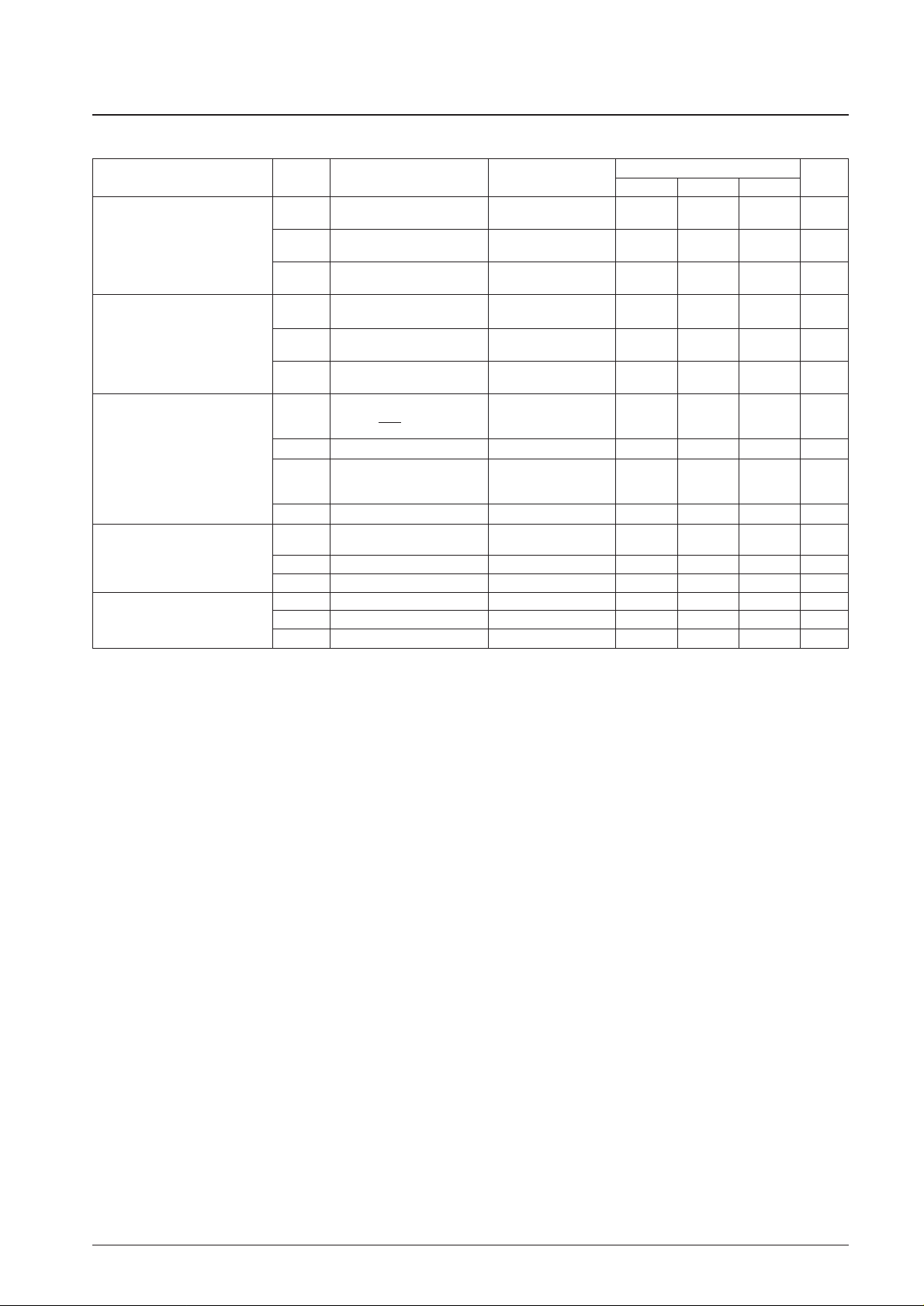
No. 7191-7/50
LC74735W
Parameter Symbol Pin Conditions
Ratings
Unit
min typ max
V
OH
1
RD2:0, GD2:0, BD2:0, V
DD
1 = 3.0 V
VDD1 – 0.8
— — V
and BLK outputs I
OH
1 = –8 mA
High-level output voltage V
OH
2 A0:17, OE, and CE
V
DD
3 = 3.0 V
VDD3 – 0.8
— — V
I
OH
2 = –8 mA
V
OH
3 A0:17, OE, and CE
V
DD
3 = 4.5 V
VDD3 – 0.8
— — V
I
OH
3 = –8 mA
V
OL
1
RD2:0, GD2:0, BD2:0, V
DD
1 = 3.0 V
— — 0.4 V
and BLK outputs I
OL
1 = 8 mA
Low-level output voltage V
OL
2 A0:17, OE, and CE
V
DD
3 = 3.0 V
— — 0.4 V
I
OL
2 = 8 mA
V
OL
3 A0:17, OE, and CE
V
DD
3 = 4.5 V
— — 0.4 V
I
OL
3 = 8 mA
CTRL1, TEST1, TEST2,
IIH1 SCLK, SIN, CS, VSYNC, VIN= VDD1 — — 10 µA
HSYNC, RST
Input current
I
IH
2 D0:11 VIN= VDD3 — — 10 µA
CTRL1, TEST1, TEST2,
IIL1 SCLK, SIN, CS, VSYNC, VIN= V
SS
–10 — — µA
HSYNC
IIL2 D0:11 VIN= V
SS
–10 — — µA
I
DD
1 VDD1
All outputs open
— — 37 mA
Operating current drain
OSCin: 40 MHz
I
DD
2 VDD2 D/A on — — 22 mA
I
DD
3 VDD3 — — 20 mA
CLK Clock frequency — — 20 MHz
D/A Vmax Maximum output voltage V
DD
2 = 3.3 V — 1 — V
Vmin Minimum output voltage V
DD
2 = 3.3 V — 0 — V
Electrical Characteristics at Ta = –30 to +85°C, VDD= 3.3 V unless otherwise specified.
Page 8

Supplementary Materials
No. 7191-8/50
LC74735W
tw(cs)
CS
tsu(cs) tw(sclk) tw(sclk) th(cs)
SCK
tsu(sin) th(sin)
SI
tword
twt
SCK
0 1 5 6 7 0 1 54 6 7
CSB
Parameter Symbol Conditions
Ratings
Unit
min typ max
Minimum input pulse width
tw (sclk) SCK 200 — — ns
tw (cs) CSB (The period CS is high) 1 — — µs
Data setup time
tsu (cs) CSB 200 — — ns
tsu (sin) SI 200 — — ns
Data hold time
th (cs) CSB 2 — — µs
th (sin) SI 200 — — ns
One word write time
tword The time to write 8 bits of data 4.2 — — µs
twt RAM data write time 1 — — µs
OSD Write (See figure 1.) at Ta = –30 to +85°C, VDD1 = 3.3 ± 0.3 V
Timing Characteristics
Figure 1 OSD Serial Data Input Timing
Page 9
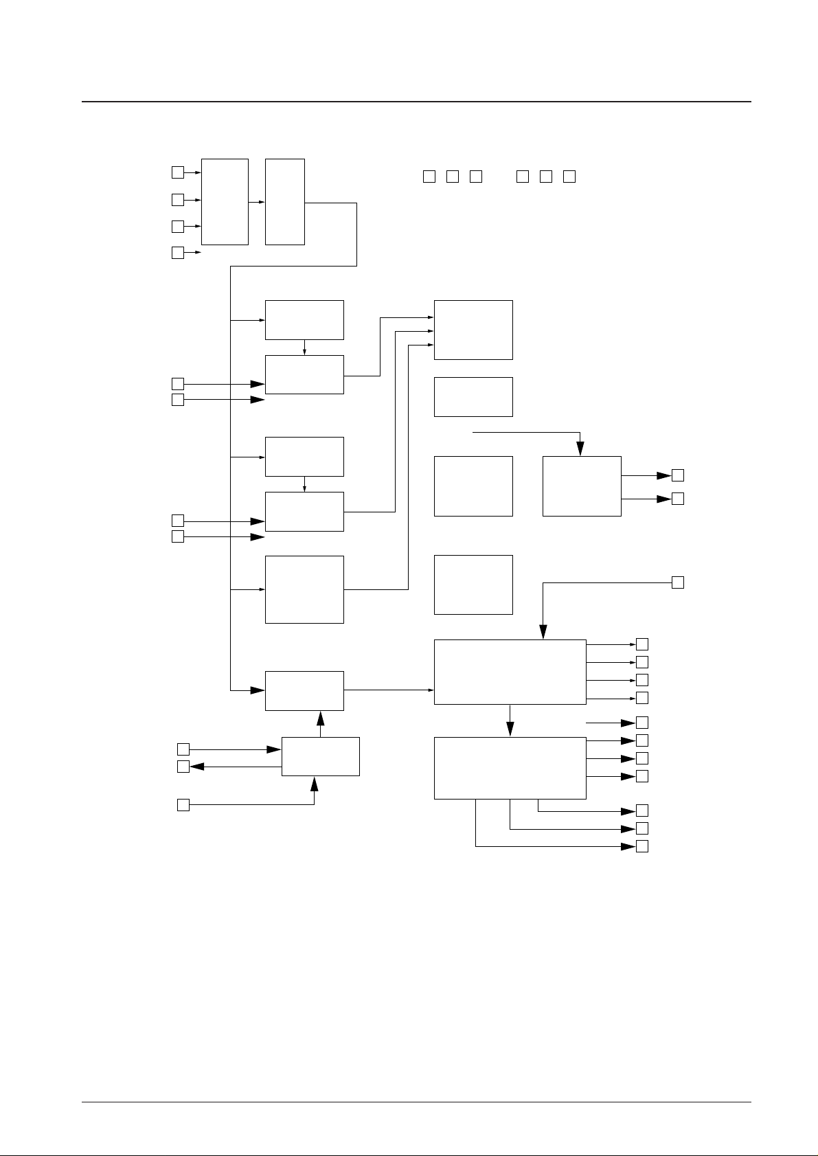
LC74735W System Block Diagram
No. 7191-9/50
LC74735W
CS
SIN
SCLK
VDD1, VDD2,VDD3 VSS1,VSS2,VSS3
RST
HSYNC
HBLK
HSYNC
HBLK
OSCin
OSCout
CTRL1
OE, CE
A0-17
D0-11
D/A
FROM
VRAM
Serial-to-
parallel
converter
16-bit
latch
+
command
decoder
Horizontal
direction
control register
Address
control circuit
Address
control circuit
External ROM
control circuit
Output control circuit
Vertical
direction
control register
Horizontal
direction
counter
Vertical
direction
counter
RAM and ROM
read and write
control
Character
size control
Timing
generator
RD2-0
GD2-0
BD2-0
BLK
CCOMP
CVREF
RREF
OUTR
ROUT
GOUT
BOUT
Page 10
No. 7191-10/50
LC74735W
Display Control Command Table
Display Control Commands
The display control commands have serial input format that consists of 8-bit units transmitted LSB first.A commands
consists of a command identification code in the first byte and data in the second and following bytes. Both a first byte
and a second byte (16 bits) must be transmitted for each command. Commands 10, 11, and 71 set the IC to continuous
write mode. (Continuous write mode is cleared by setting the CS pin high.)
First byte Second byte
Command
Command identification code
Data Data
7 6 5 4 3 2 1 0 7 6 5 4 3 2 1 0
COMMAND00 (Write address)
1 0 0 0 0 0 V3 V2 V1 V0 H5 H4 H3 H2 H1 H0
Main
COMMAND01 (Write address)
1 0 0 0 0 1 0 0 0 SV0 0 0 0 0 0 SH0
Sub (Wallpaper)
1 0 0 1 0 0 RM2
RM1(1)
0 0 at BXS BXL BXR BXU BXD
Command 10 (Character write)
(2)
CB3 CB2 CB1 CB0 CC3 CC2 CC1 CC0
Main
(3)
0 0 CT0 I/E M/G C10 C9 C8
(4)
C7 C6 C5 C4 C3 C2 C1 C0
1 0 0 1 0 1 RM2
RM1(1)
0 0 0 0 0 0 0 0
Command 11 (Character write)
(2)
0 0 0 0 0 0 0 0
Sub (Wallpaper)
(3)
0 0 CT0 I/E M/G C10 C9 C8
(4)
C7 C6 C5 C4 C3 C2 C1 C0
COMMAND20 (System control) 1 0 1 0 0 0 0 0
TSTMD2 TSTMD1
Q/W2 Q/W1
SYSRST
CTERS
SRMERS
MRMERS
COMMAND21 (Display control) 1 0 1 0 0 0 0 1
LCSOFF
BK1 BK0 SBG1 SBG0
DSPBG DSPGS DSPGM
COMMAND22 (I/O polarity control) 1 0 1 0 0 0 1 0 BLD1 BLO0 BLOP BLO1 BLO0 CKP VIP HIP
COMMAND23
(Screen background color)
1 0 1 0 0 0 1 1 0 0
BGCT1 BGCT0
BGC3 BGC2 BGC1
BGC0
COMMAND24 (I/O polarity control 2) 1 0 1 0 0 1 0 0
DSPMD1 DSPMD0
DASEL
VBLKON HBLKON
CKOP VPB
HPB
COMMAND25 (Output control 3) 1 0 1 0 0 1 0 1 0 0 0 OTM2 OTM1 OTM0
QRM1 QRM0
COMMAND30
1 0 1 1 0 0 0 0 VPM7 VPM6 VPM5 VPM4 VPM3 VPM2 VPM1
VPM0
(Vertical display start position: main)
COMMAND31
1 0 1 1 0 0 1
HPM8 HPM7 HPM6 HPM5 HPM4 HPM3 HPM2 HPM1 HPM0
(Horizontal display start position: main)
COMMAND32
1 0 1 1 0 1 0 0 VPS7 VPS6 VPS5 VPS4 VPS3 VPS2 VPS1
VPS0
(Vertical display start position: sub)
COMMAND33
1 0 1 1 0 1 1
HPS8 HPS7 HPS6 HPS5 HPS4 HPS3 HPS2 HPS1 HPS0
(Horizontal display start position: sub)
COMMAND34
1 0 1 1 1 0 0 0 VPG7 VPG6 VPG5 VPG4 VPG3 VPG2 VPG1
VPG0
(Vertical display start position: screen)
COMMAND35
1 0 1 1 1 0 1
HPG8 HPG7 HPG6 HPG5 HPG4 HPG3 HPG2 HPG1 HPG0
(Horizontal display start position: screen)
COMMAND40
1 1 0 0 0 0 0 0 0 0 0 0
SZV1 SZV0 SZH1 SZH0
(Character size control)
COMMAND41
1 1 0 0 0 1 0 0
LSZ7 LSZ6 LSZ5 LSZ4 LSZ3 LSZ2 LSZ1 LSZ0
(Character size control: line setting U)
COMMAND42
1 1 0 0 1 0 0 0
LSZ15 LSZ14 LSZ13 LSZ12 LSZ11 LSZ10 LSZ9 LSZ8
(Character size control: line setting D)
COMMAND50
1 1 0 1 0 0 0 0
BXUW BXLW
0
BXUCT0 BXUC3 BXUC2 BXUC1 BXUC0
(Box control U)
COMMAND51
1 1 0 1 0 1 0 0
BXDW BXRW
0
BXDCT0 BXDC3 BXDC2 BXDC1 BXDC0
(Box control D)
COMMAND52
1 1 0 1 1 0 0 0
LBX7 LBX6 LBX5 LBX4 LBX3 LBX2 LBX1 LBX0
(Box control: line setting U)
COMMAND53
1 1 0 1 1 1 0 0
LBX15 LBX14 LBX13 LBX12 LBX11 LBX10 LBX9 LBX8
(Box control: line setting D)
COMMAND60
1 1 1 0 0 0
BLK1 BLK0 0 0 0 EGCT0 EGC3 EGC2 EGC1 EGC0
(Border control)
COMMAND61
1 1 1 0 0 1 0 0
LFC7 LFC6 LFC5 LFC4 LFC3 LFC2 LFC1 LFC0
(Border control: line setting U)
COMMAND62
1 1 1 0 1 0 0 0
LFC15 LFC14 LFC13 LFC12 LFC11 LFC10 LFC9 LFC8
(Border control: line setting D)
COMMAND70 (Write address)
1 1 1 1 0 0 0 0
0 0 0 CIN1 CTA3 CTA2 CTA1 CTA0
Color Table
COMMAND71 (Data write)
1 1 1 1 0 1
0
RM3(1)
0 0 0 0 TCK TB2 TB1 TB0
Color Table
(2)
0 0 TG2 TG1 TG0 TR2 TR1 TR0
Page 11
Command 00 (Main screen write address set command)
No. 7191-11/50
LC74735W
• First byte
DA0 to 7 Register
Content
Notes
State Function
7 — 1
6 — 0 Command 0 identification code
5 — 0 Main screen write address setting
4 — 0
3 — 0
Sub-identification code: 0
2 — 0
1
V3
0
<MSB>
1
0 V2
0
1
• Second byte
DA0 to 7 Register
Content
Notes
State Function
7 V1
0 Main screen memory line address
1 (0 to E, hexadecimal)
6
V0
0 QVGA mode: 13 lines
<LSB>
1 WVGA mode: 15 lines
5
H5
0
<MSB>
1
4 H4
0
1
3 H3
0 Main screen memory character position address
1 (00 to 27, hexadecimal)
2 H2
0 QVGA mode: 40 characters
1 WVGA mode: 33 characters
1 H1
0
1
0
H0
0
<LSB>
1
Page 12
No. 7191-12/50
LC74735W
Command 01 (Subscreen write address set command)
• First byte
DA0 to 7 Register
Content
Notes
State Function
7 — 1
6 — 0 Command 0 identification code
5 — 0 Subscreen memory write address setting
4 — 0
3 — 0
Sub-identification code: 1
2 — 1
1 — 0
0 — 0
• Second byte
DA0 to 7 Register
Content
Notes
State Function
7 — 0
6 V0
0 Subscreen memory line address
1 (0 to 1, hexadecimal) 2 lines
5 — 0
4 — 0
3 — 0
2 — 0
1 — 0
0
H0
0 Subscreen memory character address
<LSB>
1 (0 to 1, hexadecimal) 2 characters
Page 13
No. 7191-13/50
LC74735W
Command 10 (Main screen display character data write setting command)
• First byte
DA0 to 7 Register
Content
Notes
State Function
7 — 1
6 — 0 Command 1 identification code
5 — 0 Display character data write setting
4 — 1
3 — 0
Sub-identification code 0
2 — 0
1 RM2
0
1
0 RM1
0
1
• Second byte (1)
DA0 to 7 Register
Content
Notes
State Function
7 — 0
6 — 0
5 at
0 Blinking off
Blinking specification
1 Blinking on
4 BXS
0 Protruding
Box specification: raised/recessed
1 Recessed
3 BXL
0 None
Box specification: left side
1 Box displayed
2 BXR
0 None
Box specification: right side
1 Box displayed
1 BXU
0 None
Box specification: top
1 Box displayed
0 BXD
0 None
Box specification: Bottom
1 Box displayed
When this command has been issued, the IC
remains in display character data write mode until
the CS pin is set high.
RM2 RM1 Mode
0 0 (1)(2)(3)(4) End
0 1 (1)(2)(3)(4) Continuous
1 0 (3)(4) Continuous
1 1 (2)(3)(4 Continuous
Continuous write mode selection
• Second byte (2)
DA0 to 7 Register
Content
Notes
State Function
7
CB3
0
[MSB]
1
6 CB2
0
1
5 CB1
0
1
4
CB0
0
[LSB]
1
3
CC3
0
[MSB]
1
2 CC2
0
1
1 CC1
0
1
0
CC0
0
<LSB>
1
Character background color specification
0000 to 1111, or 0 to F (hexadecimal)
Character color specification
0000 to 1111, or 0 to F (hexadecimal)
Character background color specification
When a character glyph is specified, 1 of 16 colors
may be selected.
Character color specification
When a character glyph is specified, 1 of 16 colors
may be selected.
*: This register is set to the all bits zero state when the IC is reset by the RST pin.
Page 14
No. 7191-14/50
LC74735W
• Second byte (3)
DA0 to 7 Register
Content
Notes
State Function
7 — 0
6 — 0
5 CT0
0 Color table number 1
Color table selection
1 Color table number 2
4 I/E
0 Internal ROM
ROM selection
1 External ROM
3 M/G
0 Character
Character/graphic specification
1 Graphic
2
C10
0
[MSB]
1
1 C9
0
Character code specification
1
0 C8
0
1
• Second byte (4)
DA0 to 7 Register
Content
Notes
State Function
7 C7
0
1
6 C6
0
1
5 C5
0
1
4 C4
0
1
3 C3
0
1
2 C2
0
1
1 C1
0
1
0
C0
0
[LSB]
1
Character code
Internal ROM: 512 characters
000 to 1FF (hexadecimal)
0 to 511
External ROM: 2048 characters
000 to 7FF (hexadecimal)
0 to 2047
* Transparent character specification
I/E = 0 (Internal ROM)
M/G = 0 (Character)
Code = 1FF (hexadecimal)
Character code specification
*: This register is set to the all bits zero state when the IC is reset by the RST pin.
Page 15
No. 7191-15/50
LC74735W
Command 11 (Subscreen display character data write setting command)
• First byte
DA0 to 7 Register
Content
Notes
State Function
7 — 1
6 — 0 Command 1 identification code
5 — 0 Display character data write setting
4 — 1
3 — 0
Sub-identification code 1
2 — 0
1 RM2
0
1
0 RM1
0
1
When this command has been issued, the IC
remains in display character data write mode until
the CS pin is set high.
RM2 RM1 Mode
0 0 [1][2][3][4] End
0 1 [1][2][3][4] Continuous
1 0 [3][4] Continuous
1 1 [2][3][4] Continuous
Continuous write mode selection
DA0 to 7 Register
Content
Notes
State Function
7 — 0
6 — 0
5 0
4 0
3 0
2 0
1 0
0 0
• Second byte (1)
DA0 to 7 Register
Content
Notes
State Function
7 0
6 0
5 0
4 0
3 0
2 0
1 0
0 0
• Second byte (2)
*: This register is set to the all bits zero state when the IC is reset by the RST pin.
Page 16

No. 7191-16/50
LC74735W
• Second byte (3)
DA0 to 7 Register
Content
Notes
State Function
7 — 0
6 — 0
5 CT0
0 Color table number 1
Color table selection
1 Color table number 2
4 I/E
0 Internal ROM
ROM selection
1 External ROM
3 M/G
0 Only when transparent is selected
Graphic only
1 Graphic only
2
C10
0
[MSB]
1
1 C9
0
Character code specification
1
0 C8
0
1
• Second byte (4)
DA0 to 7 Register
Content
Notes
State Function
7 C7
0
1
6 C6
0
1
5 C5
0
1
4 C4
0
1
3 C3
0
1
2 C2
0
1
1 C1
0
1
0
C0
0
[LSB]
1
Character code
Internal ROM: 512 characters
000 to 1FF (hexadecimal)
0 to 511
External ROM: 2048 characters
000 to 7FF (hexadecimal)
0 to 2047
* Transparent character specification
I/E = 0 (Internal ROM)
M/G = 0 (Character)
Code = 1FF (hexadecimal)
Character code specification
*: This register is set to the all bits zero state when the IC is reset by the RST pin.
Page 17

No. 7191-17/50
LC74735W
Command 20 (System control settings command)
• First byte
• Second byte
DA0 to 7 Register
Content
Notes
State Function
7 — 1
6 — 0 Command 2 identification code
5 1 System control settings
4 0
3 0
2 0
Sub-identification code 0
1 0
0 0
DA0 to 7 Register
Content
Notes
State Function
7 TSTMD2
0 Normal operation
1 Test mode 2
6 TSTMD1
0 Normal operation
1 Test mode 1
5 Q/W2
0 Normal mode
1 Independent mode
4 Q/W1
0 QVGA mode
1 WVGA mode
3 SYSRST
0
1 Reset all registers (All bits set to 0.)
2 CTERS
0
1 Erase the color table. (Sets all values to 00.)
0
1 SRMERS
1
Erase main RAM. (Sets all values to 00.)
Wallpaper
0
0 MRMERS
1
Erase sub-RAM. (Sets all values to 00.)
Main screen
Do not use test mode. This bit must be set to 0.
Do not use test mode. This bit must be set to 0.
Normal / Independent
QVGA / WVGA
The registers are reset when the CSB pin is low.
The reset state is cleared when the CSB pin goes high.
Applications must provide a wait time of about 1ms.
Use DSPOFF to execute this operation.
Applications must provide a wait time of about 1ms.
Use DSPOFF to execute this operation.
Applications must provide a wait time of about 1ms.
Use DSPOFF to execute this operation.
Page 18

No. 7191-18/50
LC74735W
Command 21 (Display control settings command)
• First byte
• Second byte
DA0 to 7 Register
Content
Notes
State Function
7 — 1
6 — 0 Command 2 identification code
5 — 1 Display control
4 — 0
3 — 0
2 — 0
Sub-identification code 1
1 0
0 1
DA0 to 7 Register
Content
Notes
State Function
7 LCSOFF
0 Enables stopping the LC oscillator
LC oscillator stop control
1 Disables stopping the LC oscillator
6 BK1
0
1
5 BK0
0
1
4 SBG1
0 Display before the main screen
Subscreen display specification
1 Display after the main screen
3 SBG0
0 Iterated display (wallpaper)
Subscreen display specification
1 Horizontal 2-character x vertical 2-character display (sprite)
2 DSPBG
0 Display off
Screen background color
1 Display on
1 DSPGS
0 Display off
Subscreen (wallpaper)
1 Display on
0 DSPGM
0 Display off
Main screen
1 Display on
Blinking period
Specified for screen units.
*: This register is set to the all bits zero state when the IC is reset by the RST pin.
BK1 BK0
0 0 1/16
0 1 1/32
1 0 1/64
Page 19

No. 7191-19/50
LC74735W
Command 22 (I/O polarity control settings command)
• First byte
• Second byte
DA0 to 7 Register
Content
Notes
State Function
7 — 1
6 — 0 Command 2 identification code
5 — 1 Display character data write settings
4 — 0
3 — 0
2 — 0
Extended command identification code 2
1 1
0 0
DA0 to 7 Register
Content
Notes
State Function
7 BLD1
0
1
6 BLD0
0
1
5 BLOP
0 BLK output: positive polarity
BLK output polarity selection
1 BLK output: negative polarity
4 BLO1
0
1
3 BLO0
0
1
2 CKP
0 Clock input: positive polarity
Clock input polarity selection
1 Clock input: negative polarity
1 VIP
0 VSYNC input: negative polarity
VSYNC input polarity selection
1 VSYNC input: positive polarity
0 HIP
0 HSYNC input: negative polarity
HSYNC input polarity selection
1 HSYNC input: positive polarity
BLK output delay setting
In dot clock units
*: This register is set to the all bits zero state when the IC is reset by the RST pin.
BLD1 BLD0
0 0 ±0
0 1 +1
1 0 +2
1 1 +3
BLO1 BLO0
0 0
Text + character background + wallpaper + screen background
0 1 Text + character background + wallpaper
1 0 Text + character background
1 1 Text
BLK output control
Page 20

No. 7191-20/50
LC74735W
Command 23 (Screen background color settings command)
• First byte
• Second byte
DA0 to 7 Register
Content
Notes
State Function
7 — 1
6 — 0 Command 2 identification code
5 — 1 Display character data write settings
4 — 0
3 — 0
2 — 0
Extended command identification code 3
1 1
0 1
DA0 to 7 Register
Content
Notes
State Function
7 — 0
6 — 0
5 BGCT1
0
1
4 BGCT0
0
1
3 BGC3
0
1
2 BGC2
0
1
1 BGC1
0
1
0 BGC0
0
1
Screen background color
Color table setting
T1 T0
0 0 Color table No. 2
0 1 Invalid setting
1 X Color table No. 1
Screen background color
Selects 1 of 16 values.
Screen background color
0000 to 1111
0 to F (hexadecimal)
*: This register is set to the all bits zero state when the IC is reset by the RST pin.
Page 21

No. 7191-21/50
LC74735W
Command 24 (I/O polarity control settings command)
• First byte
• Second byte
DA0 to 7 Register
Content
Notes
State Function
7 — 1
6 — 0 Command 2 identification code
5 — 1 Display character data write settings
4 — 0
3 — 0
2 — 1
Extended command identification code 4
1 0
0 0
DA0 to 7 Register
Content
Notes
State Function
7 DSPMD1
0
1
6 DSPMD0
0
1
5 D/ASEL
0 On
1 Off
4 VBLKON
0 Disabled
VBLK input selection
1 Enabled
3 HBLKON
0 Disabled
HBLK input selection
1 Enabled
2 CKOP
0 Clock output positive polarity
Clock output polarity selection
1 Clock output negative polarity
1 VBP
0 VBLK input negative polarity
VBLK input polarity selection
1 VBLK input positive polarity
0 HBP
0 HBLK input negative polarity
HBLK input polarity selection
1 HBLK input positive polarity
Main screen display area selection
Clock output polarity selection
Only valid in independent mode.
COM20 to COM2
*: This register is set to the all bits zero state when the IC is reset by the RST pin.
MD1 MD0
0 0 40 characters × 13 lines
0 1 33 characters × 15 lines
1 0 40 characters × 16 lines
D/A converter used/unused selection
Only valid in independent mode. COM20 to COM2
Page 22

No. 7191-22/50
LC74735W
Command 25 (Output control 3 settings command)
• First byte
• Second byte
DA0 to 7 Register
Content
Notes
State Function
7 — 1
6 — 0 Command 2 identification code
5 — 1 Display character data write settings
4 — 0
3 — 0
2 — 1
Extended command identification code 5
1 0
0 1
DA0 to 7 Register
Content
Notes
State Function
7 — 0
6 — 0
5 — 0
4 OTMD2
0
1
3 OTMD1
0
1
2 OTMD0
0
1
1 QRM1
0
1
0
0 QRM0
1
A0:17 output selection
OTMD2 OTMD1 OTMD0 Output
0 0 0 Normal
0 0 1 RGB No. 1
0 1 0 RGB No. 2
0 1 1 High-impedance state
ROM selection when character output is specified
in QVGA mode
QRM1 QRM0 ROM selection
0 0 ROM1
0 1 ROM2
1 0 ROM3
1 1 ROM4
*: This register is set to the all bits zero state when the IC is reset by the RST pin.
• When RGB No. 1 or RGB No. 2 is selected:
The A17:9 output is set to the
RDB2 to BD0 three-value output. (Supported by connecting external resistors.)
* It will not be possible to use external ROM in this case. (Only internal ROM can be used.)
No. 1: RGB = 000 = Black only. Here the output will go to the high-impedance state giving the middle level due to the external resistor.
For areas other than the display area, the output will be at the low level.
No. 2: When any individual color is zero, the output will go to the high-impedance state giving the middle level due to the external resistor.
For areas other than the display area, the output will be at the low level.
Page 23

No. 7191-23/50
LC74735W
Command 30 (Main screen: vertical display start position setting command)
• First byte
• Second byte
DA0 to 7 Register
Content
Notes
State Function
7
VPM7
0
(MSB)
1 The vertical display start position, VSM, is given by:
6 VPM6
0
1
5 VPM5
0
1
4 VPM4
0
1
3 VPM3
0
1
2 VPM2
0
1
1 VPM1
0
1
0
VPM0
0
(LSB)
1
7
VSM = 1H × ( ∑2nVPMn)
n=0
HSYNC
HSM
VSM
Main screen display area
VSYNC
DA0 to 7 Register
Content
Notes
State Function
7 — 1
6 — 0 Command 3 identification code
5 — 1 Main screen: vertical display start position setting
4 — 1
3 — 0
2 — 0
Extended command identification code 0
1 — 0
0 — 0
Main screen
The vertical display start position is specified by the
8 bits VPM7:0.
The weight of the LSB is 1H in QVGA mode, and
the weight of the LSB is 2H in WVGA mode
This setting applies in screen units.
Page 24

No. 7191-24/50
LC74735W
Command 31 (Main screen: horizontal display start position setting command)
• First byte
DA0 to 7 Register
Content
Notes
State Function
7 — 1
6 — 0 Command 3 identification code
5 — 1 Main screen: horizontal display start position setting
4 — 0
3 — 0
2 — 0 Extended command identification code 1
1 — 1
0
HPM8
0
(MSB)
1
• Second byte
DA0 to 7 Register
Content
Notes
State Function
7 HPM7
0
1
6 HPM6
0 The horizontal display start position, HSM, is given by:
1
5 HPM5
0
1
4 HPM4
0
1
3 HPM3
0
1
2 HPM2
0 • Setting disable range
1
1 HPM1
0
1
0
HPM0
0
(LSB)
1
8
HSM = 1Tc × ( ∑2nHPMn) + α
n=0
α = 57 Tc
Tc: The input clock frequency in operating mode.
QVGA : 00 to 0F HEX
WVGA : 00 to 07 HEX
Main screen
The horizontal display start position is specified by
the 9 bits HPM8:0.
The weight of the LSB is 1TC in QVGA mode, and
the weight of the LSB is 2TC in WVGA mode
This setting applies in screen units.
*: This register is set to the all bits zero state when the IC is reset by the RST pin.
Page 25

No. 7191-25/50
LC74735W
Command 32 (Subscreen: vertical display start position setting command)
• First byte
• Second byte
DA0 to 7 Register
Content
Notes
State Function
7
VPS7
0
(MSB)
1 The vertical display start position, VSS, is given by:
6 VPS6
0
1
5 VPS5
0
1
4 VPS4
0
1
3 VPS3
0
1
2 VPS2
0
1
1 VPS1
0
1
0
VPS0
0
(LSB)
1
7
VSS = 1H × ( ∑2nVPSn)
n=0
HSYNC
HSS
VSS
Subscreen display area
VSYNC
DA0 to 7 Register
Content
Notes
State Function
7 — 1
6 — 0 Command 3 identification code
5 — 1 Subscreen: vertical display start position setting
4 — 1
3 — 0
2 — 1 Extended command identification code 2
1 — 0
0 — 0
Subscreen (wallpaper)
The vertical display start position is specified by the
8 bits VPS7:0.
The weight of the LSB is 1H in QVGA mode, and
the weight of the LSB is 2H in WVGA mode
This setting applies in screen units.
Page 26

No. 7191-26/50
LC74735W
Command 33 (Subscreen: horizontal display start position setting command)
• First byte
DA0 to 7 Register
Content
Notes
State Function
7 — 1
6 — 0 Command 3 identification code
5 — 1 Subscreen: horizontal display start position setting
4 — 0
3 — 0
2 — 1 Extended command identification code 3
1 1
0
HPS8
0
(MSB)
1
• Second byte
DA0 to 7 Register
Content
Notes
State Function
7 HPS7
0
1
6 HPS6
0 The horizontal display start position, HSS, is given by:
1
5 HPS5
0
1
4 HPS4
0
1
3 HPS3
0
1
2 HPS2
0
1 • Setting disable range
1 HPS1
0
1
0
HPS0
0
(LSB)
1
8
HSS = 1Tc × ( ∑2nHPSn) + α
n=0
α = 14 Tc
Tc: The input clock frequency in operating mode.
Subscreen (wallpaper)
The horizontal display start position is specified by
the 9 bits HPS8:0.
The weight of the LSB is 1TC in QVGA mode, and
the weight of the LSB is 2TC in WVGA mode
This setting applies in screen units.
*: This register is set to the all bits zero state when the IC is reset by the RST pin.
QVGA : 00 to 2F HEX
WVGA : 00 to 17 HEX
Page 27

No. 7191-27/50
LC74735W
Command 34 (Screen background color: vertical display start position setting command)
• First byte
• Second byte
DA0 to 7 Register
Content
Notes
State Function
7
VPG7
0
(MSB)
1 The vertical display start position, VSG, is given by:
6 VPG6
0
1
5 VPG5
0
1
4 VPG4
0
1
3 VPG3
0
1
2 VPG2
0
1
1 VPG1
0
1
0
VPG0
0
(LSB)
1
7
VSG = 1H × ( ∑2nVPGn)
n=0
HSYNC
HSG
VSG
Screen background
color display area
VSYNC
DA0 to 7 Register
Content
Notes
State Function
7 — 1
6 — 0 Command 3 identification code
5 — 1 Screen background color: vertical display start position setting
4 — 1
3 — 1
2 — 0 Extended command identification code 4
1 — 0
0 — 0
Screen background color
The vertical display start position is specified by the
8 bits VPG7:0.
The weight of the LSB is 1H in QVGA mode, and
the weight of the LSB is 2H in WVGA mode
This setting applies in screen units.
Page 28

No. 7191-28/50
LC74735W
Command 35 (Screen background color: horizontal display start position setting command)
• First byte
DA0 to 7 Register
Content
Notes
State Function
7 — 1
6 — 0 Command 3 identification code
5 — 1 Screen background color: horizontal display start position setting
4 — 1
3 — 1
2 — 0 Extended command identification code 5
1 1
0
HPS8
0
(MSB)
1
• Second byte
DA0 to 7 Register
Content
Notes
State Function
7 HPG7
0
1
6 HPG6
0 The horizontal display start position, HSG, is given by:
1
5 HPG5
0
1
4 HPG4
0
1
3 HPG3
0
1
2 HPG2
0
1
1 HPG1
0
1
0
HPG0
0
(LSB)
1
8
HSG = 1Tc × ( ∑2nHPGn)
n=0
Tc: The input clock frequency in operating mode.
Screen background color
The horizontal display start position is specified by
the 9 bits HPG8:0.
The weight of the LSB is 1TC in QVGA mode, and
the weight of the LSB is 2TC in WVGA mode
This setting applies in screen units.
*: This register is set to the all bits zero state when the IC is reset by the RST pin.
Page 29

No. 7191-29/50
LC74735W
Command 40 (Character size control setting command)
• First byte
• Second byte
DA0 to 7 Register
Content
Notes
State Function
7 — 0
6 — 0
5 — 0
4 — 0
3 SZV1
0
1
0
2 SZV0
1
1 SZH1
0
1
0
0 SZH0
1
DA0 to 7 Register
Content
Notes
State Function
7 — 1
6 — 1 Command 4 identification code
5 — 0 Display character data write settings
4 — 0
3 — 0
Extended command identification code 0
2 — 0
1 0
0 0
Specifies the character size in the vertical direction.
This setting applies in line units.
SZV1 SZV0 Character size
0 0 1×
0 1 2×
1 0 3×
1 1 4×
Specifies the character size in the horizontal
direction.
This setting applies in line units.
SZH1 SZH0 Character size
0 0 1×
0 1 2×
1 0 3×
1 1 4×
*: This register is set to the all bits zero state when the IC is reset by the RST pin.
Page 30

No. 7191-30/50
LC74735W
Command 41 (Character size line U control setting command)
• First byte
• Second byte
DA0 to 7 Register
Content
Notes
State Function
7 LSZ7
0 Do not set for line 8.
1 Set for line 8.
6 LSZ6
0 Do not set for line 7.
1 Set for line 7.
5 LSZ5
0 Do not set for line 6.
1 Set for line 6.
4 LSZ4
0 Do not set for line 5.
1 Set for line 5.
3 LSZ3
0 Do not set for line 4.
1 Set for line 4.
2 LSZ2
0 Do not set for line 3.
1 Set for line 3.
1 LSZ1
0 Do not set for line 2.
1 Set for line 2.
0 LSZ0
0 Do not set for line 1.
1 Set for line 1.
DA0 to 7 Register
Content
Notes
State Function
7 — 1
6 — 1 Command 4 identification code
5 — 0 Character size line U control
4 — 0
3 — 0
Extended command identification code 1
2 — 1
1 — 0
0 — 0
Character size line setting control
Upper lines
Page 31

No. 7191-31/50
LC74735W
Command 42 (Character size line D control setting command)
• First byte
• Second byte
DA0 to 7 Register
Content
Notes
State Function
7 LSZ15
0 Do not set for line 16.
1 Set for line 16.
6 LSZ14
0 Do not set for line 15.
1 Set for line 15.
5 LSZ13
0 Do not set for line 14.
1 Set for line 14.
4 LSZ12
0 Do not set for line 13.
1 Set for line 13.
3 LSZ11
0 Do not set for line 12.
1 Set for line 12.
2 LSZ10
0 Do not set for line 11.
1 Set for line 11.
1 LSZ9
0 Do not set for line 10.
1 Set for line 10.
0 LSZ8
0 Do not set for line 9.
1 Set for line 9.
DA0 to 7 Register
Content
Notes
State Function
7 — 1
6 — 1 Command 4 identification code
5 — 0 Character size line D control
4 — 0
3 — 1
Extended command identification code 2
2 — 0
1 — 0
0 — 0
Character size line setting control
Lower lines
Page 32

No. 7191-32/50
LC74735W
Command 50 (Box control: U setting command)
• First byte
DA0 to 7 Register
Content
Notes
State Function
7 — 1
6 — 1 Command 5 identification code
5 — 0 Display character data write settings
4 — 1
3 — 0
Extended command identification code 0
2 — 0
1 — 0
0 — 0
• Second byte
DA0 to 7 Register
Content
Notes
State Function
7 BXUW
0 Box display: upper side is 1 dot.
1 Box display: upper side is 2 dot.
6 BXLW
0 Box display: left side is 1 dot.
1 Box display: left side is 2 dot.
5 — 0
0 Color table No. 1
4 BXUCT0
1 Color table No. 2
3 BXUC3
0
1
2 BXUC2
0
1
1 BXUC1
0
1
0 BXUC0
0
1
Box display: upper side
Dot width. This setting applies in line units.
Box display: left side
Dot width. This setting applies in line units.
Box display: upper side
Color table specification
This setting applies in line units.
Box display: upper side
Color specification
This setting applies in line units.
Box display: upper side color specification
0000 to 1111
0 to F (hexadecimal)
*: This register is set to the all bits zero state when the IC is reset by the RST pin.
Page 33

No. 7191-33/50
LC74735W
Command 51 (Box control: D setting command)
• First byte
DA0 to 7 Register
Content
Notes
State Function
7 — 1
6 — 1 Command 5 identification code
5 — 0 Display character data write settings
4 — 1
3 — 0
Extended command identification code 1
2 — 1
1 — 0
0 — 0
• Second byte
DA0 to 7 Register
Content
Notes
State Function
7 BXDW
0 Box display: lower side is 1 dot.
1 Box display: lower side is 2 dot.
6 BXRW
0 Box display: right side is 1 dot.
1 Box display: right side is 2 dot.
5 — 0
0 Color table No. 1
4 BXDCT0
1 Color table No. 2
3 BXDC3
0
1
2 BXDC2
0
1
1 BXDC1
0
1
0 BXDC0
0
1
Box display: lower side
Dot width. This setting applies in line units.
Box display: right side
Dot width. This setting applies in line units.
Box display: lower side
Color table specification
This setting applies in line units.
Box display: lower side
Color specification
This setting applies in line units.
Box display: lower side color specification
0000 to 1111
0 to F (hexadecimal)
*: This register is set to the all bits zero state when the IC is reset by the RST pin.
Page 34

No. 7191-34/50
LC74735W
Command 52 (Box control: U line setting command)
• First byte
• Second byte
DA0 to 7 Register
Content
Notes
State Function
7 LBX7
0 Do not set for line 8.
1 Set for line 8.
6 LBX6
0 Do not set for line 7.
1 Set for line 7.
5 LBX5
0 Do not set for line 6.
1 Set for line 6.
4 LBX4
0 Do not set for line 5.
1 Set for line 5.
3 LBX3
0 Do not set for line 4.
1 Set for line 4.
2 LBX2
0 Do not set for line 3.
1 Set for line 3.
1 LBX1
0 Do not set for line 2.
1 Set for line 2.
0 LBX0
0 Do not set for line 1.
1 Set for line 1.
DA0 to 7 Register
Content
Notes
State Function
7 — 1
6 — 1 Command 5 identification code
5 — 0 Character size: line U control
4 — 1
3 — 1
Extended command identification code 2
2 — 0
1 — 0
0 — 0
Box control line setting control
Upper lines
Page 35

No. 7191-35/50
LC74735W
Command 53 (Character size: Line D control setting command)
• First byte
• Second byte
DA0 to 7 Register
Content
Notes
State Function
7 LBX15
0 Do not set for line 16.
1 Set for line 16.
6 LBX14
0 Do not set for line 15.
1 Set for line 15.
5 LBX13
0 Do not set for line 14.
1 Set for line 14.
4 LBX12
0 Do not set for line 13.
1 Set for line 13.
3 LBX11
0 Do not set for line 12.
1 Set for line 12.
2 LBX10
0 Do not set for line 11.
1 Set for line 11.
1 LBX9
0 Do not set for line 10.
1 Set for line 10.
0 LBX8
0 Do not set for line 9.
1 Set for line 9.
DA0 to 7 Register
Content
Notes
State Function
7 — 1
6 — 1 Command 5 identification code
5 — 0 Character size line D control
4 — 1
3 — 1
Extended command identification code 3
2 — 1
1 — 0
0 — 0
Box control line setting control
Lower lines
Page 36

No. 7191-36/50
LC74735W
Command 60 (Border control settings command)
• First byte
• Second byte
DA0 to 7 Register
Content
Notes
State Function
7 — 1
6 — 1 Command 6 identification code
5 — 1 Display character data write settings
4 — 0
3 — 0
Extended command identification code 0
2 — 0
1 BLK1
0
1
0 BLK0
0
1
Border mode specification
This setting applies in line units.
BLK1 BLK0
0 0 Normal display
0 1 Border
1 0 Shadow 1 (lower side)
1 1 Shadow 2 (lower and right sides)
DA0 to 7 Register
Content
Notes
State Function
7 — 0
6 — 0
5 — 0
0 Color table No. 1
4 EGCT0
1 Color table No. 2
3 EGC3
0
1
2 EGC2
0
1
1 EGC1
0
1
0 EGC0
0
1
Border display
Color table specification
This setting applies in line units.
Border display color specification
This setting applies in line units.
Border display: color specification
0000 to 1111
0 to F (hexadecimal)
*: This register is set to the all bits zero state when the IC is reset by the RST pin.
Page 37

No. 7191-37/50
LC74735W
Command 61 (Border control U line settings command)
• First byte
• Second byte
DA0 to 7 Register
Content
Notes
State Function
7 LFC7
0 Do not set for line 8.
1 Set for line 8.
6 LFC6
0 Do not set for line 7.
1 Set for line 7.
5 LFC5
0 Do not set for line 6.
1 Set for line 6.
4 LFC4
0 Do not set for line 5.
1 Set for line 5.
3 LFC3
0 Do not set for line 4.
1 Set for line 4.
2 LFC2
0 Do not set for line 3.
1 Set for line 3.
1 LFC1
0 Do not set for line 2.
1 Set for line 2.
0 LFC0
0 Do not set for line 1.
1 Set for line 1.
DA0 to 7 Register
Content
Notes
State Function
7 — 1
6 — 1 Command 6 identification code
5 — 1 Character size: line U control
4 — 0
3 — 0
Extended command identification code 1
2 — 1
1 — 0
0 — 0
Border control line settings control
Upper lines
Page 38

No. 7191-38/50
LC74735W
Command 62 (Border control D line settings command)
• First byte
• Second byte
DA0 to 7 Register
Content
Notes
State Function
7 LFC15
0 Do not set for line 16.
1 Set for line 16.
6 LFC14
0 Do not set for line 15.
1 Set for line 15.
5 LFC13
0 Do not set for line 14.
1 Set for line 14.
4 LFC12
0 Do not set for line 13.
1 Set for line 13.
3 LFC11
0 Do not set for line 12.
1 Set for line 12.
2 LFC10
0 Do not set for line 11.
1 Set for line 11.
1 LFC9
0 Do not set for line 10.
1 Set for line 10.
0 LFC8
0 Do not set for line 9.
1 Set for line 9.
DA0 to 7 Register
Content
Notes
State Function
7 — 1
6 — 1 Command 6 identification code
5 — 1 Character size: line D control
4 — 0
3 — 1
Extended command identification code 2
2 — 0
1 — 0
0 — 0
Border control line settings control
Lower lines
Page 39

No. 7191-39/50
LC74735W
DA0 to 7 Register
Content
Notes
State Function
7 —
6 —
5 —
4 CTN1
0 Color table No. 1 selected
1 Color table No. 2 selected
3
CTA3
0
<MSB>
1
2 CTA2
0
1
1 CTA1
0
1
0
CTA0
0
<LSB>
1
Color table selection
No. 1 or No. 2
Color table address
0 to 15
0 to F (hexadecimal) 16 values
Addresses of the color tables
Command 70 (Color table write address setting command)
• First byte
• Second byte
DA0 to 7 Register
Content
Notes
State Function
7 — 1
6 — 1 Command 7 identification code
5 — 1 Color table write address setting
4 — 1
3 — 0
Sub-identifier code 0
2 — 0
1 — 0
0 — 0
Page 40

No. 7191-40/50
LC74735W
Command 71 (Color table data write setting command)
• First byte
DA0 to 7 Register
Content
Notes
State Function
7 — 1
6 — 1 Command 7 identification code
5 — 1 Display character data write setting
4 — 1
3 — 0
Sub-identifier code 1
2 — 1
1 — 0
0
0 RM3
1
• Second byte (1)
When this command has been issued, the IC
remains in display character data write mode until
the CS pin is set high.
RM3 Mode
0 [1][2] End
1 [1][2] Continuous
Continuous write mode selection
DA0 to 7 Register
Content
Notes
State Function
7 — 0
6 — 0
5 — 0
4 — 0
3 TOK
0 Color
1 Transparent (BLK output: low)
2 TB2
0
1
1 TB1
0
1
0 TB0
0
1
Color table
B output
000 to 111
0 to 7 (hexadecimal)
Color table setting B
• Second byte (2)
DA0 to 7 Register
Content
Notes
State Function
7 — 0
6 — 0
5 TG2
0
1
4 TG1
0
1
3 TG0
0
1
2 TR2
0
1
1 TR1
0
1
0 TR0
0
1
Color table
G output
000 to 111
0 to 7 (hexadecimal)
Color table setting G
Color table
R output
000 to 111
0 to 7 (hexadecimal)
Color table setting R
*: This register is set to the all bits zero state when the IC is reset by the RST pin.
When transparent is selected, the BLK output is set to the low level. (Transparent state)
The RGB outputs are values from the color table.
The transparent specification is best for color table 1, address 0000.
Since the data is set to all zeros by a RAM clear operation,
The RGB output will be 000 (black) and the BLK output will be 1.
Transparent is specified by setting the TOK bit to 1. (The BLK output will go to the low level.)
Page 41

Display Structure
The display screen consists of a 40-character × 15-line grid.
QVGA mode (12 × 18 dot characters)
40-character × 13-line QVGA panel (480 × 234)
WVGA mode (12 × 16 dot characters)
33-character × 15-line WVGA panel (800 × 480)
Up to a maximum of 600 characters can be displayed.
If the character size is increased, the number of characters that can be displayed will decrease to be fewer than 600
characters.
Display memory is addressed by specifying a line address (0 to 14 (decimal) and a character position address (0 to 39
(decimal)).
No. 7191-41/50
LC74735W
40 Characters
00
00
01
02
03
04
05
06
07
08
09
10
11
12
13
14
0
1
2
3
4
5
6
7
8
9
A
B
C
D
E
HEX
01 02 03 04 05 06 07 08 09 10 11 12 13 14 15 16 17 18 19 20 21 22 23 24 25 26 27 28 29 30 31 32 33 34 35 36 37 38 39
00 01 02 03 04 05 06 07 08 09 0A 0B 0C 0D 0E 0F 10 11 12 13 14 15 16 17 18 19 1A 1B 1C 1D 1E 1F 20 21 22 23 24 25 26 27
HEX
15 Rows
Display Structure (Display memory address)
Page 42

Operational Description
Command transfer method
Overview
(1) Commands are transferred in 8-bit units, LSB first.
Always send a first byte and a second byte (16 bits).
(2) Command 10 (Main RAM write)
Command 11 (Wallpaper write)
Command 71 (Color table write)
When these commands specify continuous mode (RM2, 1 RM3), the IC is locked in continuous write mode.
(Continuous write mode is cleared by setting the CS pin high.)
Writing data to VRAM
(1) Write start address specification
Use command 00 to set the write start address.
V3:0: Vertical direction, H5:0: Horizontal direction
(2) Data write
Continuous write mode differs depending on the write mode specification. (RM1, RM2)
1. Normal (RM2 = 0, RM1 = 0: initial state) *Continuous mode not used*
-- COM10-1 10-2-1 10-2-2 10-2-3 10-2-4 command wait state --
2. Write continuous (RM2 = 0, RM1 = 1): Mode 2
COM10-1 10-2-1 10-2-2 10-2-3 10-2-4
3. Write continuous (RM2 = 1, RM1 = 0): Mode 3
COM10-1 10-2-1 10-2-2 10-2-3 10-2-4 10-2-3 10-2-4
4. Write continuous (RM2 = 1, RM1 = 1): Mode 4
COM10-1 10-2-1 10-2-2 10-2-3 10-2-4 10-2-2 10-2-3 10-2-4
*: In modes 2, 3, and 4, the IC remains locked in continuous write mode until the CS pin is set high.
• The write address is automatically incremented.
• The write address is retained unless the IC is reset or a new write address is issued.
No. 7191-42/50
LC74735W
Page 43

Color table write
(1) Write start address specification
Use command 70 to set the color table write start address.
CTN :1: Color table specification (No.1, No.2), CTA3:0: Address specification
No. 7191-43/50
LC74735W
No.1
R G B
XXX0000
0001
0010
1110
1111
XXX
Address
XXX
No.2
R G B
XXX0000
0001
0010
1110
1111
XXX XXX
(2) Data write
Continuous write mode differs depending on the write mode specification. (RM3)
1. Normal (RM3 = 0: initial state) *Continuous mode not used*
-- COM71-1 71-2-1 71-2-2 command wait state ---
2. Write continuous (RM3 = 1) mode
COM71-1 71-2-1 71-2-2
*: In mode 2, the IC remains locked in continuous write mode until the CS pin is set high.
• The write address is automatically incremented.
• The write address is retained unless the IC is reset or a new write address is issued.
Page 44

Display Format
Color specification related items
(1) When a character is specified
Color specification for the character color (character area) and character background color (outside the character
area)
Character color: One of 16 colors
Character background color: One of 16 colors
Color tables: Table No. 1 or No. 2 specified by CT1:0. (COM1-2-3: VRAM)
→ One of 32 types
No. 7191-44/50
LC74735W
Character color
Specified by CC0 to CC3: One of 16 colors
(COM1-2-2: VRAM)
Character background color
Specified by CB0 to CB3: One of 16 colors
(COM1-2-2: VRAM)
(2) When a graphic is specified
Color is specified in dot units (12 × 18 or 12 × 16)
One of 16 colors (FROM)
Color tables: Table No. 1 or No. 2 specified by CT1:0. (COM1-2-3: VRAM)
→ One of 32 types
Specified by FROM: One of 16 types
Page 45

No. 7191-45/50
LC74735W
Display control related items
(1) Blinking: In character units
1. Normal at1 = 0 (COM1-2-1: VRAM)
2. Blinking at1 = 1
Display alternates between normal and transparent with the blinking period. (COM21-2: BK1, 0)
(2) Border display: Only valid for font specified characters
1. Border color: One of 16 colors (COM60-2 EGC3 to 0)
Color table specification (COM60-2 EGCT0)
→ One of 32 types
2. Border mode control (COM60-1 BLK1, 0)
i. Border
(3) Character size: Specified in line units
The character size is specified as 1x to 4x independently for the vertical and horizontal directions.
(COM40-2)
ii. Shadow 1: lower
iii. Shadow 2: lower + right
Page 46

No. 7191-46/50
LC74735W
Box display (raised/recessed)
(1) Raised/recessed specification: In character units (COM10-2-1 BXS)
(2) Left side - displayed/undisplayed specification: in character units (COM10-2-1 BXL)
(3) Right side - displayed/undisplayed specification: in character units (COM10-2-1 BXR)
(4) Upper side - displayed/undisplayed specification: in character units (COM10-2-1 BXU)
(5) Lower side - displayed/undisplayed specification: in character units (COM10-2-1 BXD)
(6) Color specification: In line units
COM50 (Upper side)
COM51 (Lower side)
BXUC3:0: One of 16 colors
BXDC3:0: One of 16 colors
Color table specification
BXUCT0
BXDCT0
→ One of 32 types
Dot width specification: 1 or 2 dots
Each of left, right, upper, and lower can be specified independently. (BXLW BXRW BXUW BXDW)
Raised
12 dots
Recessed
18 dots
or
16 dots
Page 47

No. 7191-47/50
LC74735W
Screen structure
Screen background color
Wallpaper display screen
Main screen
• QVGA mode (12 × 18 dot characters)
40-character × 13-line QVGA panel
• WVGA mode (12 × 16 dot characters)
33-character × 15-line WVGA panel
• For each screen: Display on/off (transparent) can be specified independently.
• For each screen: The display start position can be specified independently.
The wallpaper display screen and the main screen are displayed up to the horizontal direction start position. (The
XXX clock is required.)
Page 48

No. 7191-48/50
LC74735W
Display format
(1) QVGA
18H
Character specification
12 dots
Graphic
12 dots
(2) WVGA
32H
Character specification
24 dots
Graphic
24 dots
Each dot is 2 × 2 pixels
(A 12 × 16 structure
magnified 2× in both
the horizontal and
vertical directions)
ROM structure
Internal ROM (512 characters)
(1) Character font
QVGA: 12 × 18-dot structure
WVGA: 24 × 32-dot structure, i.e. 12 × 16 times 4
(2) Graphics
CQVGA: 12 × 18-dot structure
WVGA: 12 × 16-dot structure, i.e. displayed magnified 2× in both the horizontal and vertical directions.
Note that the contents of ROM differs for QVGA and WVGA.
(That is, different ROMs for QVGA and WVGA must be created.)
Page 49

No. 7191-49/50
LC74735W
External ROM (2048 characters)
(1) Conditions
Use a 16-bit 4M ROM with an access time less than 3 times the dot clock period
Example: DCLK = 50 MHz = 20 ns period × 3 = under 60 ns
DCLK = 10 MHz = 100 ns period × 3 = under 300 ns
(2) ROM map
[1]
A1 to A0
00
12 bits
A6 to A2
QVGA mode
18 bits
WVGA mode
16 bits
D15 to D12, D11 to D0
01 10 11
• Address
A17 to A7 (10 bits) = 2048 characters = character codes
• Data
Unused Used
[2] [3] [4]
(3) Display appearance
1. QVGA: 1 character = 12 × 18 dots
Character font: [1]
Graphics: [1] + [2] + [3] + [4]
2. WVGA: 1 character = 12 × 16 dots
Character font: [1] [2]
[3] [4]
Graphics: ([1] + [2] + [3] + [4]) displayed magnified 2× in both the horizontal and vertical directions.
[1] [2]
12 12
[3]
16
16 [4]
[1]+[2]
+[3]+[4]
× 2
12 12
16
16
Page 50

PS No. 7191-50/50
LC74735W
This catalog provides information as of April, 2002. Specifications and information herein are subject to
change without notice.
Specifications of any and all SANYO products described or contained herein stipulate the performance,
characteristics, and functions of the described products in the independent state, and are not guarantees
of the performance, characteristics, and functions of the described products as mounted in the customer’s
products or equipment. To verify symptoms and states that cannot be evaluated in an independent device,
the customer should always evaluate and test devices mounted in the customer’s products or equipment.
SANYO Electric Co., Ltd. strives to supply high-quality high-reliability products. However, any and all
semiconductor products fail with some probability. It is possible that these probabilistic failures could
give rise to accidents or events that could endanger human lives, that could give rise to smoke or fire,
or that could cause damage to other property. When designing equipment, adopt safety measures so
that these kinds of accidents or events cannot occur. Such measures include but are not limited to protective
circuits and error prevention circuits for safe design, redundant design, and structural design.
In the event that any or all SANYO products (including technical data, services) described or contained
herein are controlled under any of applicable local export control laws and regulations, such products must
not be exported without obtaining the export license from the authorities concerned in accordance with the
above law.
No part of this publication may be reproduced or transmitted in any form or by any means, electronic or
mechanical, including photocopying and recording, or any information storage or retrieval system,
or otherwise, without the prior written permission of SANYO Electric Co., Ltd.
Any and all information described or contained herein are subject to change without notice due to
product/technology improvement, etc. When designing equipment, refer to the “Delivery Specification”
for the SANYO product that you intend to use.
Information (including circuit diagrams and circuit parameters) herein is for example only; it is not
guaranteed for volume production. SANYO believes information herein is accurate and reliable, but
no guarantees are made or implied regarding its use or any infringements of intellectual property rights
or other rights of third parties.
 Loading...