

Page 1
Ordering number : ENN*4245A
D2599TH (OT)/12993JN No. 4245-1/16
Preliminary
LC74711
SANYO Electric Co.,Ltd. Semiconductor Company
TOKYO OFFICE Tokyo Bldg., 1-10, 1 Chome, Ueno, Taito-ku, TOKYO, 110-8534 JAPAN
Controller LSI for On-screen Displays
CMOS LSI
Any and all SANYO products described or contained herein do not have specifications that can handle
applications that require extremely high levels of reliability, such as life-support systems, aircraft’s
control systems, or other applications whose failure can be reasonably expected to result in serious
physical and/or material damage. Consult with your SANYO representative nearest you before using
any SANYO products described or contained herein in such applications.
SANYO assumes no responsibility for equipment failures that result from using products at values that
exceed, even momentarily, rated values (such as maximum ratings, operating condition ranges, or other
parameters) listed in products specifications of any and all SANYO products described or contained
herein.
Overview
The LC74711 is a CMOS LSI for applications involving
microcomputer control of on-screen character and
graphics displays. Built-in character ROM supplies 128
alphanumerics and each character is generated in a 12
by 18 pixel format. The display is capable of supporting
a maximum of 288 characters within a 24 characters by
12 line array.
Functions and Applications
(1) Screen construction:
24 characters X 12 lines
(2) Number of characters displayed:
Maximum 288 characters capacity
(3) Display control ROM (line ROM):
64 lines (line unit control: 24 character construction)
(4) Display RAM:
176 characters (supporting extended character
selection)
(5) Character construction: 12 (horizontal) X 18
(vertical) pixels
(6) Character set: 128 types of characters
(7) Character size:
4 horizontal types and 4 vertical types
(8) Display starting position: 64 types horizontally and
64 types vertically
(9) Blinking: Character units
(10) Blinking types: 2 types with approximate 1.0 s and
0.5 s cycles and 3-type selection for 25%, 50% and
75% duty
(11) Blanking: Font complete blanking (12
X 18 pixels)
(12) Background color: 8 background tints (during
internal synchronizing operation: 4 fsc when using
crystal oscillator)
(13) External control input: Serial data input
(14) Synchronizing signal: Internal synchronizing,
supports external synchronizing changeover
(15) Built-in synchronizing separator circuit
(16) Video output: NTSC system composite video
output
(17) Superimpose: Characters superimposed over
composite video output
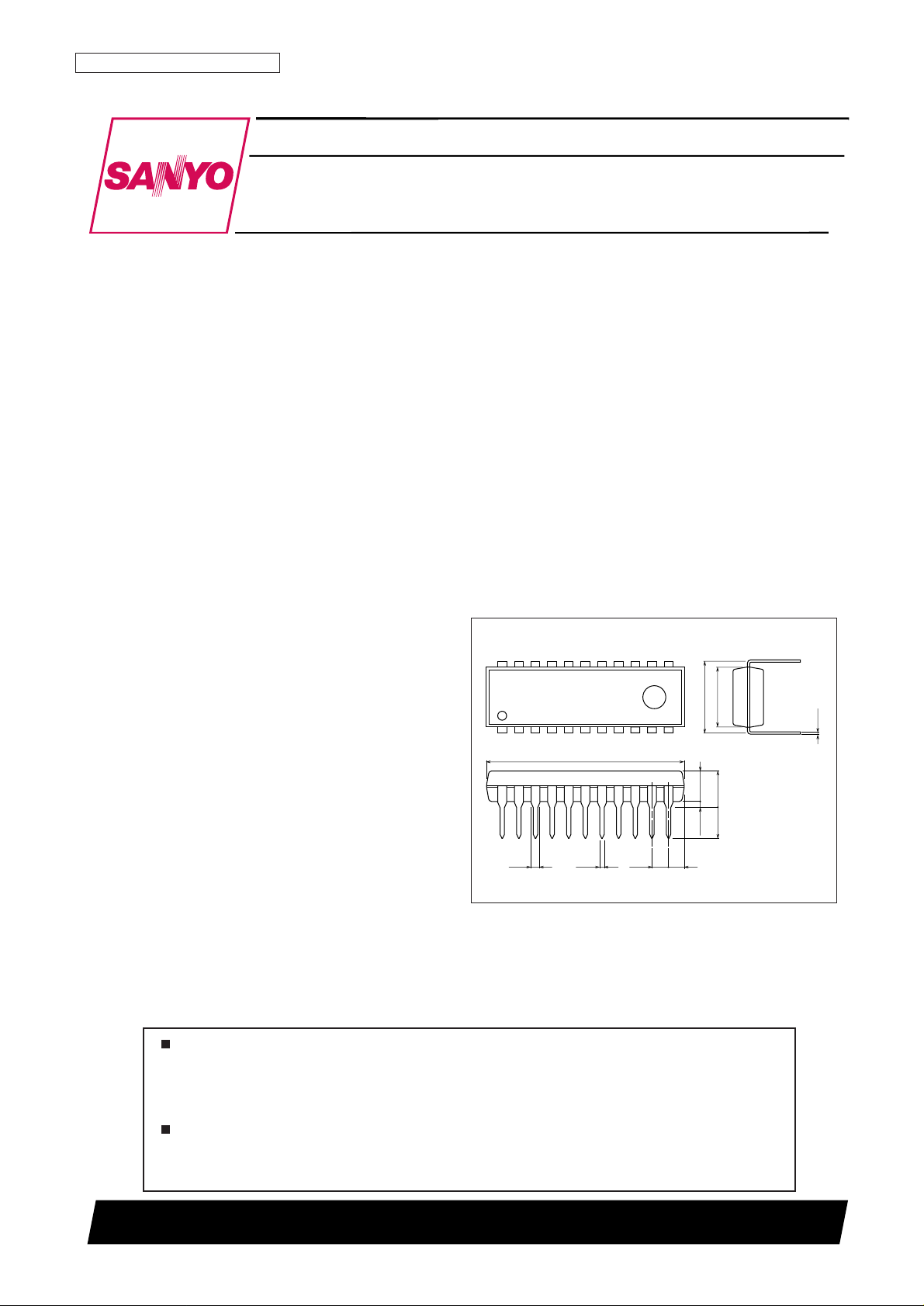
(18) Package: DIP-22S
21.2
0.95 0.48
1.71.78
3.9max
0.51min
6.4
7.62
3.3
3.25
0.25
111
22 12
SANYO: DIP22S
[LC74711]
Package Dimensions
unit : mm
3059-DIP22S
Page 2
LC74711
No. 4245-2/16
Specifications
Absolute Maximum Ratings
Item Symbol Conditions/Pins Ratings Unit
Maximum supply voltage V
DD
max V
DD1
, V
DD2
VSS–0.3 to VSS+7.0 V
Maximum input voltage V
IN
max All input pins VSS–0.3 to VDD+0.3 V
Maximum output voltage V
OUT
max VSS–0.3 to VDD+0.3 V
Allowable power dissipation Pd max Ta = 25°C 300 mW
Operating temperature Topr –30 to +70 °C
Storage temperature Tstg –40 to +125 °C
Allowable Operating Ranges at Ta = –30 to +70°C
Item Symbol Conditions/Pins
Ratings
Unit
min typ max
Supply voltage
V
DD1
V
DD1
pin 4.5 5.0 5.5 V
V
DD2
V
DD2
pin 4.5 5.0 1.27V
DD1
V
Input “H” level voltage V
IH
CS, SIN, RST, SCLK, SEPIN pin 0.8V
DD1
V
DD1
+0.3 V
Input “L” level voltage V
IL
CS, SIN, RST, SCLK, SEPIN pin VSS–0.3 0.2V
DD1
V
Composite video input voltage
V
IN1
CVINpin 2V
P-P
V
V
IN2
SYNI pin 2V
P-P
2.5V
P-P
Oscillation frequency
F
OSC1
Xtal oscillation pin (2 fsc) 7.159 MHz
F
OSC2
Xtal oscillation pin (4 fsc) 14.318 MHz
F
OSC3
LC oscillation pin (when using LC oscillation)
5 7 10 MHz
Electrical Characteristics at Ta = –30 to +70 °C, default of V
DD1
= 5 V
Item Symbol Pins Conditions
Ratings
Unit
min typ max
Output off leak current I
leak
CV OUT pin 10 µA
Output “H” level voltage V
OH1
SEP OUT pin V
DD1
= 4.5V, IOH= –1.0mA 3.5 V
Output “L” level voltage V
OL1
SEP OUT pin V
DD1
= 4.5V, IOL= 1.0mA 1.0 V
Input current
I
IH
VIN= V
DD1
1 µA
I
IL
OSCIN pin VIN= V
SS
–1 µA
I
DD1
V
DD1
pin
All output are OPEN
10 mA
Xtal = 14.318MHz, LC = 7MHz
I
DD2
V
DD2
pin V
DD2
= 5.0V 15 mA
Timing Characteristics at Ta = –30 to +70°C, V
DD1
= 5 ±0.5 V
Item Symbol Conditions/Pins
Ratings
Unit
min typ max
Input minimum pulse width
t
w
(SCLK) SCLK pin 200 ns
t
w
(CS) CS pin (with CS set to “H” period) 1 µs
Data setup time
t
su
(CS) CS pin 200 ns
t
su
(SIN) SIN pin 200 ns
Data hold time
t
h
(CS) CS pin 2 µs
t
h
(SIN) SIN pin 200 ns
Single word and write time
t
word
16-bit write time 10 µs
t
wt
RAM data write time 1 µs
Current consumption
during operation
CS, SIN, RST,
SCLK, SEPIN pin
Page 3
LC74711
No. 4245-3/16
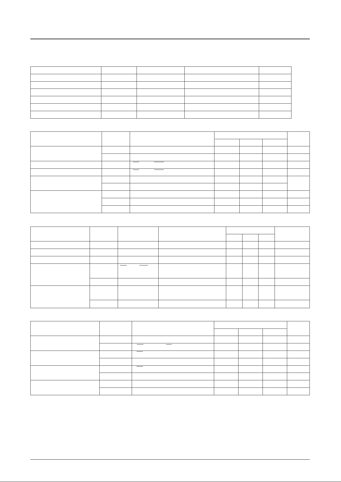
Serial Data Input Timing
Pin Assignment
Page 4
LC74711
No. 4245-4/16
Pin Functions
Pin No. Pin Symbol Pin name Functions
1 V
SS1
Ground pin Pin for connecting to ground (GND) (grounding pin for digital system).
2 Xtal IN
Xtal oscillation pin
Pin for connecting to capacitor or crystal of crystal oscillator for internal
3 Xtal OUT
synchronizing signal oscillation applications.
4 TEST Test output pin Pin for test data output.
5 RST Reset input pin Pin for system reset input (hysteresis input).
6 SCLK Clock input pin Pin for clock input using serial data input (hysteresis input).
7 SIN Data input pin Pin for serial data input (hysteresis input). Input in 16-bit units.
8 CS Enable input pin
Pin for enable input for serial data processing (hysteresis input). “L” serial data
input switches to enable.
9 LVBK
Blanking level adjustment
input pin
Pin for level input for blanking level adjusting.
10 LVCHA
Character level adjustment
input pin
Pin for level input for character level adjusting.
11 V
DD2
Supply pin Pin for power supply for adjusting signal level of composite video (power
supply for analog system).
12 CV OUT Video signal output pin Pin for composite video signal output.
13 NC Non connection.
14 CV IN Video signal input pin Pin for composite video signal input.
15 V
DD1
Power supply pin Pin for power supply (+5V).
16 SYNI
Synchronizing separator
circuit input pin
Pin for input of separator circuit composite synchronizing signal.
17 SEPC
Synchronizing separator
circuit adjustment pin
Pin for adjusting synchronizing separator circuit (connecting capacitor).
18 SEP OUT Composite synchronizing
signal output pin
Pin for output of composite synchronizing signal for synchronizing separator circuit
.
19 SEP IN
Vertical synchronizing
signal input pin
Pin for input of vertical synchronizing signal and integrating output signal of SEP OUT
pin. Applied when connecting an integrating circuit to the SEP OUT pin.
20 OSC OUT
LC oscillation pin
Pin for connecting a capacitor or oscillator coil for pixel clock generation and
21 OSC IN
character output applications.
22 V
DD1
Power supply pin (+5V) Pin for power supply (+5V).
Page 5
LC74711
No. 4245-5/16
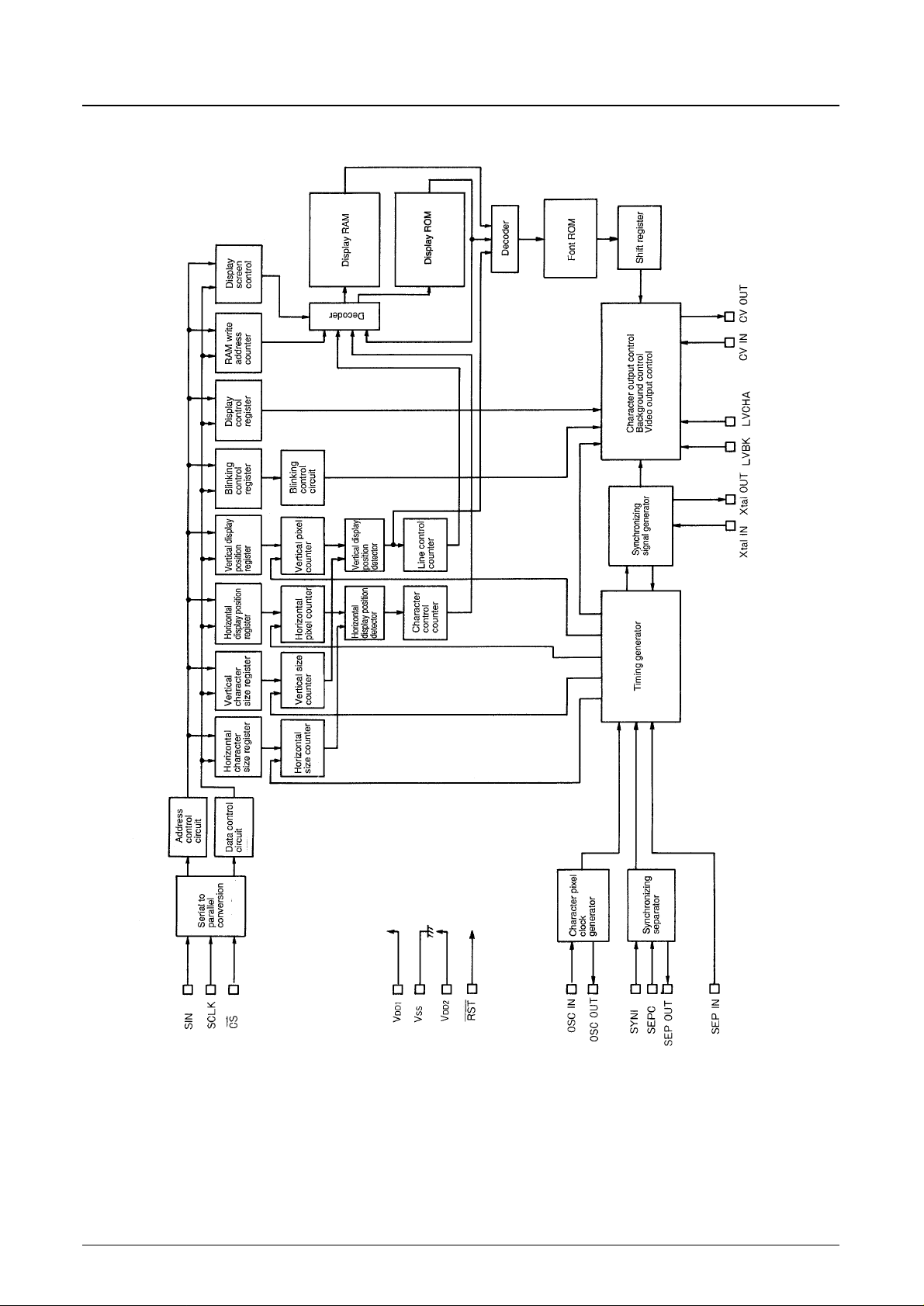
System Block Diagram
Page 6

LC74711
No. 4245-6/16
Screen Construction
Display mode supports 24 characters and 12 lines.
Maximum number of displayed characters is 288 characters.
When character size is enlarged, the maximum number of characters displayed is reduced to less than 288 characters.
Display line ROM (12-line setting) or display RAM (176 characters).
• Displays using line ROM specify the fixed character set.
• Extended character set are available using display RAM and program setting of characters.
Page 7

LC74711
No. 4245-7/16
Memory Construction (display RAM and control RAM)
Memory addresses and data 16-bit processing.
Addresses 0 (000
HEX
) to 175 (OAF
HEX
) are reserved for display memory (RAM) data.
Addresses 176 (0B0
HEX
) to 191 (0BF
HEX
) are reserved for display control register data.
Page 8

LC74711
No. 4245-8/16
(1) Address 188 (0 BC
HEX
)
Note: * When reset using the RST pin, all registers are set to 0 (zero).
Page 9

LC74711
No. 4245-9/16
(2) Address 189 (0 BD
HEX
)
Note: * When reset using the RST pin, all registers are set to 0 (zero).
Page 10

LC74711
No. 4245-10/16
(3) Address 190 (0 BE
HEX
)
DA Register
Contents
Notes
0 to C Name
Setting Function
0 PHASE0
0
1
1 PHASE1
0
1
2 PHASE2
0
1
3 —
0
1
4 —
0
1
5 SYSRST
0
1 All registers reset and display set to off
6 —
0
1
7 DSPON
0 Character display off
1 Character display on
8 OSCSTP
0 Crystal oscillator circuit and LC oscillator circuit is not stopped
1 Crystal oscillator circuit and LC oscillator circuit is stopped
9
2fsc
0 Clock frequency 2 fsc
/4fsc
1 Clock frequency 4 fsc
A
LC
0 Using LC oscillation for pixel clock
/XTAL
1 Using crystal oscillation for pixel clock
B
INT
0 Interlaced (312.5 H/1 field)
/NON
1 Non-interlaced (313 H/1 field)
C —
0
1
Note: * When reset using the RST pin, all registers are set to 0 (zero).
Background tint
Background color phase responding
to color burst.
CS pin resets for “L” and cancels
reset using “H”.
External synchronizing mode enabled
only when character display is off.
Crystal oscillator circuit oscillation
frequency.
When the LC oscillation circuit is not
used, OSC IN pin is fixed at V
DD
.
Changeover is permitted between
interlace and non-interlaced displays.
PHASE2 PHASE1 PHASE0 Background tint
0 0 0 π/2
0 0 1 π
0 1 0 3π/2
0 1 1 In-phase
1 0 0 π/4
1 0 1 3π/4
1 1 0 5π/4
1 1 1 7π/4
Page 11

(4) Address 191 (0BF
HEX
)
DA Register
Contents
Notes
0 to C Name
Setting Function
0 BCOL
0 With background tint (only enabled with internal synchronizing)
1 No background tint (background level setting only)
1 CBOFF
0 Burst signal always output
1 When BCOL is set to “H”, burst signal also does not output
2 EX
0 External synchronizing
1 Internal synchronizing
3 BLINK0
0
1
4 BLINK1
0
1
5 BLINK2
0 Blinking cycle approximately 0.5 s
1 Blinking cycle approximately 1 s
6 —
0
1
7 BLK0
0
1
8 BLK1
0
1
9 —
0
1
A
—
0
1
B TSTMOD
0 Normal operation mode
1 Test operation mode
C —
0
1
Note: * When reset using the RST pin, all registers are set to 0 (zero).
BLK0
0 1
BLK1
0 Blanking off Character size
1 Trimming size Total overall size
LC74711
No. 4245-11/16
HSYNC and VSYNC signal changeover to
external or internal supported
.
Blinking duty comparative variability.
Variable blinking cycle.
Variable blanking size.
Fixes to zero (0) condition.
BLINK0
0 1
BLINK1
0 Blinking off 25% duty
1 50% duty 75% duty
Page 12

LC74711
No. 4245-12/16
Memory Construction (Display Line ROM)
Memory addresses are arrayed within 0 (000
HEX
) to 1535 (5FF
HEX
) and have an 8-bit data construction.
DA Register
Contents
Notes
0 to 8 Name
Setting Function
0 ADR0
0
1
1 ADR1
0
1
2 ADR2
0
1
3 ADR3
0
1
4 ADR4
0
1
5 ADR5
0
1
6 ADR6
0
1
7 ROM/
0 Character ROM is accessed and read directly
RAM 1 Character ROM is accessed and read through display RAM
Character ROM address setting
When display control RAM is specified, DA7 equals “1” and
ADR0 to ADR6 are set to “0”
Character ROM address setting range is 0 to 127 (7F
HEX
)
Page 13

LC74711
No. 4245-13/16
Line Address Table for Display Line ROM
Page 14

LC74711
No. 4245-14/16
Screen Construction (Sample Display)
Setting of 12-line display using display line ROM (64 lines).
Within line ROM, setting of extended characters is made available through display control RAM.
Display control RAM addresses are automatically allocated to display array from 0 to 175 (AF
HEX
).
Input Timing of External Control Data
Input format is set at 16-bit, serial input for address and data input.
Address and Data Serial Input
➀ Address Input with 16-bit Construction
Lower 8 bits are reserved for address assignments while the upper 8 bits are fixed to “0”.
➁ Data Input with 16-bit Construction
• Lower 8 bits having addresses 000
HEX
through 0AF
HEX
are reserved for data assignments while the upper 8 bits
are fixed to “0”.
• Lower 11 bits having addresses 0B0
HEX
through 0BB
HEX
are reserved for data assignments while the upper 5
bits are fixed to “0”.
• Lower 12 bits having addresses 0BC
HEX
through 0BF
HEX
are reserved for data assignments while the upper 4
bits are fixed to “0”.
➂ Data Input Format
After the onset of CS, the first 16 bits are processed as address information, and thereafter information is processed
as data in 16-bit units. Addresses are automatically allocated in 16-bit increments.
Page 15

LC74711
No. 4245-15/16
Composite Video Signal Output Level (Internal generation level: synchronization chip level = 0.8 V)
Output Level Output Voltage (VDC) V
DD2
= 5.000V
DC
Character level 2.650
Background color “H” level 2.075
Burst “L” level 1.700
Background color “L” level 1.500
Trimming level 1.500
Pedestal level 1.375
Burst “L” level 1.050
Synchronization chip level 0.800
Page 16

LC74711
PS No. 4245-16/16
This catalog provides information as of December, 1999. Specifications and information herein are
subject to change without notice.
Specifications of any and all SANYO products described or contained herein stipulate the performance,
characteristics, and functions of the described products in the independent state, and are not guarantees
of the performance, characteristics, and functions of the described products as mounted in the customer’s
products or equipment. To verify symptoms and states that cannot be evaluated in an independent device,
the customer should always evaluate and test devices mounted in the customer’s products or equipment.
SANYO Electric Co., Ltd. strives to supply high-quality high-reliability products. However, any and all
semiconductor products fail with some probability. It is possible that these probabilistic failures could
give rise to accidents or events that could endanger human lives, that could give rise to smoke or fire,
or that could cause damage to other property. When designing equipment, adopt safety measures so
that these kinds of accidents or events cannot occur. Such measures include but are not limited to protective
circuits and error prevention circuits for safe design, redundant design, and structural design.
In the event that any or all SANYO products (including technical data, services) described or contained
herein are controlled under any of applicable local export control laws and regulations, such products must
not be exported without obtaining the export license from the authorities concerned in accordance with the
above law.
No part of this publication may be reproduced or transmitted in any form or by any means, electronic or
mechanical, including photocopying and recording, or any information storage or retrieval system,
or otherwise, without the prior written permission of SANYO Electric Co., Ltd.
Any and all information described or contained herein are subject to change without notice due to
product/technology improvement, etc. When designing equipment, refer to the “Delivery Specification”
for the SANYO product that you intend to use.
Information (including circuit diagrams and circuit parameters) herein is for example only; it is not
guaranteed for volume production. SANYO believes information herein is accurate and reliable, but
no guarantees are made or implied regarding its use or any infringements of intellectual property rights
or other rights of third parties.
 Loading...