

Page 1
Any and all SANYO products described or contained herein do not have specifications that can handle
applications that require extremely high levels of reliability, such as life-support systems, aircraft’s
control systems, or other applications whose failure can be reasonably expected to result in serious
physical and/or material damage. Consult with your SANYO representative nearest you before using
any SANYO products described or contained herein in such applications.
SANYO assumes no responsibility for equipment failures that result from using products at values that
exceed, even momentarily, rated values (such as maximum ratings, operating condition ranges,or other
parameters) listed in products specifications of any and all SANYO products described or contained
herein.
CMOS IC
Character and Pattern Display Control IC
Ordering number:ENN3725
LC7470
SANYO Electric Co.,Ltd. Semiconductor Company
TOKYO OFFICE Tokyo Bldg., 1-10, 1 Chome, Ueno, Taito-ku, TOKYO, 110-8534 JAPAN
Overview
Character and pattern display control IC for TV screen. A
character dot configuration is 12 × 18. The IC has 64 inter-
nal character ROMs and displays up to 288 characters (24
characters × 12 lines) on a TV screen. It can be controlled
by a microcontroller.
Function and Applications
• Screen Display Mode: 24 characters × 12 lines
• Number of display characters: 288 characters (max.)
• Display control ROM (line ROM):
64 lines (line control: 24-character line)
• Display RAM:
176 characters (used for specifying variable characters)
• Character configuration:
12 (horizontal) × 18 (vertical) dots
• Number of character types: 64 types
• Character size:
Horizontal direction: 4, Vertical direction: 4
• Display start position:
Horizontal direction: 64, Vertical direction: 64
• Blinking mode: Character blinking
• Display ON/OFF mode:
ON/OFF cycle; 1.0 second and 0.5 second. Duty cycle;
25%, 50% and 75%
• Blanking mode: Entire font area (12 × 18 dots)
• Background colors: 4 (at internal SYNC. operation mode)
• External control input: Serial data input
• Synchronous signal: Selectable: Internal and External
• Internal SYNC. separation circuit available.
• Video output: NTSC-format composite output
• Superimpose function:
Superimposes character output on composite video
output
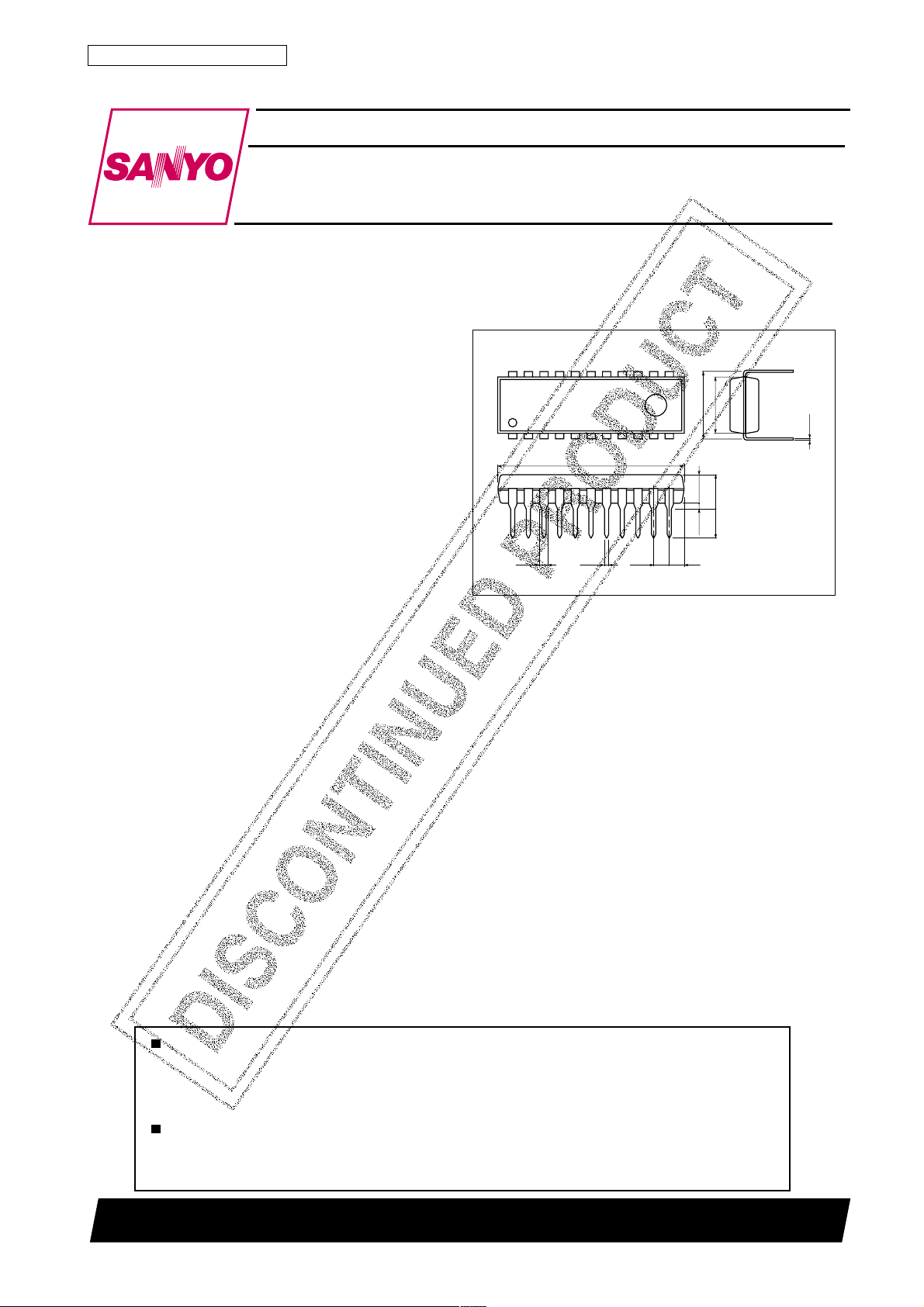
Package Dimensions
unit:mm
3059-DIP22S
[LC7470]
22 12
6.4
7.62
111
0.95 0.48
21.2
1.78
3.25
0.51min
1.7
3.9max
3.3
SANYO : DIP22S
0.25
71901TN (KT)/8290JN, TA, KI (AC) No.3725–1/13
Page 2
LC7470
Specifications
Absolute Maximum Ratings
retemaraPlobmySnoitidnoCsgnitaRtinU
egatlovylppusmumixaMV
egatlovtupnimumixaMV
egatlovtuptuomumixaMV
noitapissidrewopelbawollAxamdP 003Wm
erutarepmetgnitarepOrpoT – 07+ot03
erutarepmetegarotSgtsT – 521+ot04
Reommended Operating Conditions at Ta = –30 to +70˚C
retemaraPlobmySnoitidnoC
egatlovylppuS
egatlovlevel-hgihtupnIV
egatlovlevel-woltupnIV
egatlovtupnioedivetisopmoC
ycneuqerfnoitallicsO
V
V
V
V
F
F
F
NI
DD
2HI
2LI
1NI
2NI
TUO
1DD
2DD
1CSO
2CSO
3CSO
V
V,
1DD
2DD
sniptupnillAV
Ta = 25˚C
VniP
1DD
VniP
2DD
VC
NI
INYSniPp-pV2p-pV5.2
nipnoitallicsoCL7zHM
VSS– Vot3.0
– Vot3.0
SS
VSS– Vot3.0
sgnitaR
nimpytxam
5.40.55.5V
5.40.5
KLCS,TSR,NIS,SCsniP
KLCS,TSR,NIS,SCsniP
f4ta(nipnoitallicsolatX
)13.41zHM
CSO
f2ta(nipnoitallicsolatX
)61.7zHM
CSO
8.0V
VSS– 3.0
1DD
V
p-pV2
0.7+V
SS
3.0+V
1DD
3.0+V
1DD
72.1V
1DD
3.0+
1DD
2.0V
1DD
˚C
˚C
tinU
V
V
V
V
Electrical Characteristics at Ta = –30 C to +70˚C, and VDD = 5V, unless other noted
retemaraPlobmySnoitidnoC
tnerrucegakaelffo-tuptuOI
egatlovlevel-hgihtuptuOV
egatlovlevel-woltuptuOV
tnerructupnI
niardtnerrucgnitarepOI
I
I
VC
kael
1HI
1LI
HI
LI
DD
TUO
PES
V
,TUO
PES
V
,TUO
V,NICSO
NIV=SS
I,V5.4=
DD
I,V5.4=
DD
Am0.1=5.3V
HO
Am0.1=0.1V
LO
V,NIPES,KLCS,TSR,NIS,SC
NIV=DD
Timing Characteristics at Ta = –30 to +70˚C, VDD = 5±0.5V
retemaraPlobmySnoitidnoC
htdiwesluptupnimuminiM
emitputesataD
emitdlohataD
doirepetirwdrow-1
t
t
t
t
t
t
t
drow
t
tw
KLCS002sn
)KLCS(w
)SC(w
SC002sn
)SC(us
NIS002sn
)NIS(us
SC2sµ
)SC(h
NIS002sn
)NIS(h
)doireplevel-H=SC(SC1sµ
doirepetirwatadtib-6101sµ
doirepetirwatadMAR1sµ
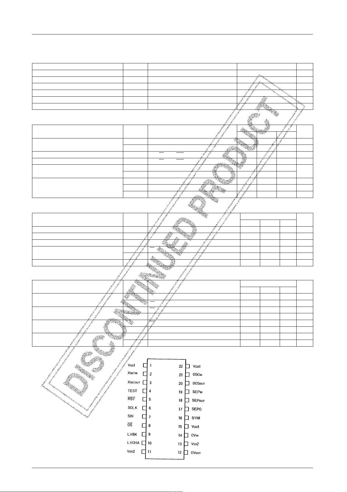
Pin Assignment
sgnitaR
nimpytxam
01Aµ
1Aµ
–1Aµ
51Am
sgnitaR
nimpytxam
tinU
tinU
Top view
No.3725–2/13
Page 3
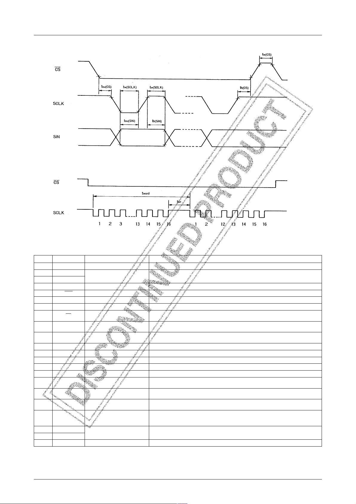
Serial Data Input Timings
LC7470
Pin Description
.oNniPlobmysniPemaNniPsnoitcnuF
1V
2IatX
3IatX
4TSETniptseTniptuptuotseT
5TSRniptupniteseRniptupnitesermetsyS
6KLCSniptupnikcolCtupniatadlairesrofniptupnikcolC
7NISniptupniataD detroppussitupniatadtib-61laireS.niptupniatadlaireS
8SCniptupnielbanE
9KBVL
01AHCVL
11V
21VC
31V
41VC
51V
61INYS
71CPES
81PES
91PES
02CSO
12CSO
22V
1SS
NI
TUO
2DD
TUO
2SS
NI
1DD
TUO
NI
TUO
NI
1DD
nipdnuorG)gnidnuorglatigid(nipDNG
nipnoitallicsolatX
tnemtsujda
tnemtsujda
nipdnuorG)gnidnuorggolana(nipDNG
niptuptuo
niptupni
levelknalbrofniptupnI
levelretcarahcrofniptupnI
nipylppusrewoProfnipylppusrewoP )ylppusrewopgolana(slevellangisoedivetisopmocgnitsujda
niptuptuolangisoediVlangisoedivetisopmocrofniptuptuO
niptupnilangisoediVlangisoedivetisopmocrofniptupnI
nipegatlovylppuSnipegatlovylppuS)V5+(
niptnemtsujdatiucric
)V5+(nipegatlovylppuS)V5+(egatlovylppuS
noitarapeslangissuonorhcnyS
noitarapeslangissuonorhcnyS
langissuonorhcnysetisopmoC
langissuonorhcnyslacitreV
niptupnitiucric
nipnoitallicsoCL skcolctodtuptuoretcarahcetarenegotroticapacdnaliocagnitcennocrofsnipnoitallicsO
slangissuonorhcnys
delbanesitupni
eveLslevelknalbgnitsujdarofniptupnil
eveLslevelretcarahcgnitsujdarofniptupnil
)nip
lanretnietarenegotroticapacdnarotallicsolatsyrcagnitcennocrofsnipnoitallicsO
atadlaireseht,)wolevitca(evitcasemocebnipsihtfI.tupniatadlairesrofniptupnielbanE
tiucricnoitarapeslangissuonorhcnysrofniptupnI
sihtotdetcennocsiroticapacA(tiucricnoitarapeslangissuonorhcnysrofniptnemtsujdA
tiucricnoitarapeslangissuonorhcnysrofniptuptuolangissuonorhcnysetisopmoC
ybdetarenegsinipsihtotlangistupniehT.niptupnilangissuonorhcnyslacitreV
nipNIPESehtdnanipTUOPES
ehtneewtebtiucriclargetninaddA.nipTUOPESehtmorflangistuptuoehtgnitargetni
No.3725–3/13
Page 4
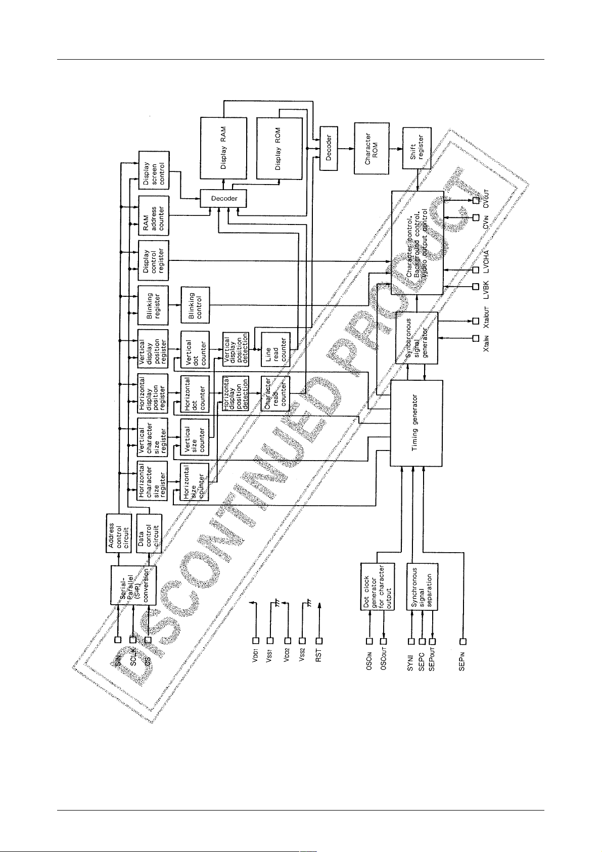
System Block Diagram
LC7470
No.3725–4/13
Page 5

LC7470
Display Screen
The maximum display screen consists of horizontal 24 characters and vertical 12 lines. The numbe of display characters
is 288 (max.). The display characters can consist of display line R OM (12 lines) data and display RAM (176 characters).
• Fixed characters can be specified by making an access to the display line ROM.
• Variable characters can be generated by programming the display RAM.
No.3725–5/13
Page 6

LC7470
Memory Configuration (display RAM and control RAM)
Memory address and data signals consist of 16 bits.
Address range from 0D (000h) to 175D (0AFh) used as the display RAM.
Address range from 176D (0B0h) to 191D (0BFh) is used as the display control register data area.
tiB
AD
FADE
sserddA
000
00000000
)h000(
AD
DADCADB
AD
AAD9AD8AD7
AD
6AD5AD4
KNILB
05C4C3C2C1C0C
AD
3AD2AD1AD0
skrameR
571
00000000
)hFA0(
671
0000-
)h0B0(
771
0000-
)h1B0(
871
0000-
)h2B0(
971
0000-
)h3B0(
081
0000-
)h4B0(
181
0000-
)h5B0(
281
0000-
)h6B0(
381
0000-
)h7B0(
481
0000-
)h8B0(
581
0000-
)h9B0(
681
0000-
)hAB0(
781
0000-
)hBB0(
881
0000
)hCB0(
981
0000
)hDB0(
091
0000
)hEB0(
191
0000
)hFB0(
ARDA9RDA8RDA7RDA6RDA5RDA4RDA3RDA2RDA1RDA0RDA
ARDA9RDA8RDA7RDA6RDA5RDA4RDA3RDA2RDA1RDA0RDA
ARDA9RDA8RDA7RDA6RDA5RDA4RDA3RDA2RDA1RDA0RDA
ARDA9RDA8RDA7RDA6RDA5RDA4RDA3RDA2RDA1RDA0RDA
ARDA9RDA8RDA7RDA6RDA5RDA4RDA3RDA2RDA1RDA0RDA
ARDA9RDA8RDA7RDA6RDA5RDA4RDA3RDA2RDA1RDA0RDA
ARDA9RDA8RDA7RDA6RDA5RDA4RDA3RDA2RDA1RDA0RDA
ARDA9RDA8RDA7RDA6RDA5RDA4RDA3RDA2RDA1RDA0RDA
ARDA9RDA8RDA7RDA6RDA5RDA4RDA3RDA2RDA1RDA0RDA
ARDA9RDA8RDA7RDA6RDA5RDA4RDA3RDA2RDA1RDA0RDA
ARDA9RDA8RDA7RDA6RDA5RDA4RDA3RDA2RDA1RDA0RDA
ARDA9RDA8RDA7RDA6RDA5RDA4RDA3RDA2RDA1RDA0RDA
ZSH
ZSH
13
03
ZSV
ZSV
13
03
INI
--
NON
TST
--
DOM
Blinking
KNILB
05C4C3C2C1C0C
ZSH
ZSH
ZSH
12
02
ZSV
ZSV
12
02
CSO
PTS
KLB
1
ZSH
11
01
ZSV
ZSV
11
01
PSD
-
NO
KLB
-
0
Character code
5PH4PH3PH2PH1PH0PH
5PV4PV3PV2PV1PV0PV
SYS
---
TSR
KNILB
KNILB
2
1
KNILB
0
1
XE
-
aeraMARyalpsiD
MORenilyalpsiD
eniltsrifehtfo
MORenilyalpsiD
enildnocesehtfo
MORenilyalpsiD
enildrihtehtfo
MORenilyalpsiD
enilhtruofehtfo
MORenilyalpsiD
enilhtfifehtfo
MORenilyalpsiD
enilhtxisehtfo
MORenilyalpsiD
MORenilyalpsiD
enilhthgieehtfo
MORenilyalpsiD
enilhtninehtfo
MORenilyalpsiD
enilhtnetehtfo
MORenilyalpsiD
MORenilyalpsiD
enilhtflewtehtfo
ESAHP
ESAHP
0
LOCB
retsigerlortnoC
retcarahctsriF.noitacificeps
retcarahctsriF.noitacificeps
retcarahctsriF.noitacificeps
retcarahctsriF.noitacificeps
retcarahctsriF.noitacificeps
retcarahctsriF.noitacificeps
retcarahctsriF.noitacificeps
enilhtnevesehtfo
retcarahctsriF.noitacificeps
retcarahctsriF.noitacificeps
retcarahctsriF.noitacificeps
retcarahctsriF.noitacificeps
enilhtneveleehtfo
retcarahctsriF.noitacificeps
.noitisopyalpsidlatnoziroH
.ezisretcarahclatnoziroH
.noitisopyalpsidlacitreV
.ezisretcarahclacitreV
.ctednalangisoediV
No.3725–6/13
Page 7

LC7470
Memory Configuration (display RAM and control RAM)
Memory address and data signals consist of 16 bits.
Address range from 0D (000h) to 175D (0AFh) used as the display RAM.
Address range from 176D (0B0h) to 191D (0BFh) is used as the display control register data area.
tiB
AD
FADE
sserddA
000
00000000
)h000(
AD
DADCADB
AD
AAD9AD8AD7
AD
6AD5AD4
KNILB
05C4C3C2C1C0C
AD
3AD2AD1AD0
skrameR
571
00000000
)hFA0(
671
0000-
)h0B0(
771
0000-
)h1B0(
871
0000-
)h2B0(
971
0000-
)h3B0(
081
0000-
)h4B0(
181
0000-
)h5B0(
281
0000-
)h6B0(
381
0000-
)h7B0(
481
0000-
)h8B0(
581
0000-
)h9B0(
681
0000-
)hAB0(
781
0000-
)hBB0(
881
0000
)hCB0(
981
0000
)hDB0(
091
0000
)hEB0(
191
0000
)hFB0(
INI
ARDA9RDA8RDA7RDA6RDA5RDA4RDA3RDA2RDA1RDA0RDA
ARDA9RDA8RDA7RDA6RDA5RDA4RDA3RDA2RDA1RDA0RDA
ARDA9RDA8RDA7RDA6RDA5RDA4RDA3RDA2RDA1RDA0RDA
ARDA9RDA8RDA7RDA6RDA5RDA4RDA3RDA2RDA1RDA0RDA
ARDA9RDA8RDA7RDA6RDA5RDA4RDA3RDA2RDA1RDA0RDA
ARDA9RDA8RDA7RDA6RDA5RDA4RDA3RDA2RDA1RDA0RDA
ARDA9RDA8RDA7RDA6RDA5RDA4RDA3RDA2RDA1RDA0RDA
ARDA9RDA8RDA7RDA6RDA5RDA4RDA3RDA2RDA1RDA0RDA
ARDA9RDA8RDA7RDA6RDA5RDA4RDA3RDA2RDA1RDA0RDA
ARDA9RDA8RDA7RDA6RDA5RDA4RDA3RDA2RDA1RDA0RDA
ARDA9RDA8RDA7RDA6RDA5RDA4RDA3RDA2RDA1RDA0RDA
ARDA9RDA8RDA7RDA6RDA5RDA4RDA3RDA2RDA1RDA0RDA
ZSH
ZSH
13
03
ZSV
ZSV
13
03
--
NON
TST
--
DOM
Blinking
KNILB
05C4C3C2C1C0C
ZSH
ZSH
ZSH
12
02
ZSV
ZSV
12
02
CSO
PTS
KLB
1
ZSH
11
01
ZSV
ZSV
11
01
PSD
-
NO
KLB
-
0
Character code
5PH4PH3PH2PH1PH0PH
5PV4PV3PV2PV1PV0PV
SYS
---
TSR
KNILB
KNILB
2
1
KNILB
0
1
XE
-
aeraMARyalpsiD
MORenilyalpsiD
eniltsrifehtfo
MORenilyalpsiD
enildnocesehtfo
MORenilyalpsiD
enildrihtehtfo
MORenilyalpsiD
enilhtruofehtfo
MORenilyalpsiD
enilhtfifehtfo
MORenilyalpsiD
enilhtxisehtfo
MORenilyalpsiD
MORenilyalpsiD
enilhthgieehtfo
MORenilyalpsiD
enilhtninehtfo
MORenilyalpsiD
enilhtnetehtfo
MORenilyalpsiD
MORenilyalpsiD
enilhtflewtehtfo
ESAHP
ESAHP
0
LOCB
retsigerlortnoC
retcarahctsriF.noitacificeps
retcarahctsriF.noitacificeps
retcarahctsriF.noitacificeps
retcarahctsriF.noitacificeps
retcarahctsriF.noitacificeps
retcarahctsriF.noitacificeps
retcarahctsriF.noitacificeps
enilhtnevesehtfo
retcarahctsriF.noitacificeps
retcarahctsriF.noitacificeps
retcarahctsriF.noitacificeps
retcarahctsriF.noitacificeps
enilhtneveleehtfo
retcarahctsriF.noitacificeps
.noitisopyalpsidlatnoziroH
.ezisretcarahclatnoziroH
.noitisopyalpsidlacitreV
.ezisretcarahclacitreV
.ctednalangisoediV
No.3725–6/13
Page 8

LC7470
(2) Address 189D (0BDH)
AD
Cot0
0
11PV
22PV
33PV
44PV
5
601ZSV
711ZSV
802ZSV
912ZSV
A03ZSV
B13ZSV
C-
emanretsigeR
0PV
)BSL(
5PV
)BSM(
sutatSnoitcnuF
0
1
0
1
0
1
0
1
0
1
0
1
0
1
0
1
0
1
0
1
0
1
0
1
0
1
VS=H×(4∑2nVPn)
11ZSV
12ZSV
13ZSV
:swollofsadetaluclac
5
n=0
01ZSV
0T1
1T3
02ZSV
0T1
1T3
03ZSV
0T1
1T3
*: If the RST pin becomes active (the IC is reset), the contents of all the registers will be set to “0”.
stnetnoC
ebnacSVeht,SVehtsadenifedsinoitisoptratsyalpsidlacitrevafI
elcyceslupnoitazinorhcnyslatnoziroH:H
01
tod1/T2
C
tod1/T4
C
01
tod1/T2
C
tod1/T4
C
01
tod1/T2
C
tod1/T4
C
tod1/
C
tod1/
C
tod1/
C
tod1/
C
tod1/
C
tod1/
C
.0PVot
.H4
enil
skrameR
noitisoptratsyalpsidlacitrevehT
5PVstibxisgnisuybdeificepssi
fothgiewtibasah)0PV(BSLehT
tsrifehtrofezisretcarahclacitreV
enildnoces
htflewtotdriht
ehtrofezisretcarahclacitreV
senilrofezisretcarahclacitreV
No.3725–8/13
Page 9

LC7470
(3) Address 190D (0BEH)
AD
Cot0
00ESAHP
11ESAHP
2-
3-
4-
5TSRSYS
6-
7NOPSD
8PTSCSO
9-
A-
B
C-
emanretsigeR
/TNI
NON
sutatSnoitcnuF
0
1
0
1
0
1
0
1
0
1
0
1detavitcanisiedomyalpsidehtdnatesererasretsigerehtllA
0
1
0FFOretcarahC
1NOretcarahC
0
1
0
1
0
1
0)dleif1/H5.262(ecalretnI
1)dleif1/H362(ecalretni-noN
0
1
1ESAHP0ESAHProlocdnuorgkcaB
00
01
103π 2/
11 esahp-nI
detavitcani
detavitcani
*: If the RST pin becomes active (the IC is reset), the contents of all the registers will be set to “0”.
stnetnoC
π 2/
π
siedomyalpsidehtfietatspotsaretnetonseodtiucricnoitallicsoehT
siedomyalpsidehtfietatspotsehtsretnetiucricnoitallicsoehT
skrameR
rolocdnuorgkcaB
siCIeht,L=levelnipSChtiW
HotsegnahclevelnipehtfI.teser
desaelereblliwteserCIeht
noitallicsolatsyrcehtpotsoT
tiucricnoitallicsoCLdnatiucric
:noitcelesedomnoitarepoyalpsiD
ecalretni-nondnaecalretni
(4) Address 191D (0BFH)
AD
Cot0
0LOCB
1-
2XE
30KNILB
41KNILB
52KNILB
6-
70KLB
81KLB
9-
A-
BDOMTST
C-
emanretsigeR
sutatSnoitcnuF
0
1)ylnoelbatsujdaleveldnuorgkcab(gnirolocdnuorgkcabevitcanI
0
1
0noitazinorhcnyslanretxE
1noitazinorhcnyslanretnI
0
1
0
1
0dnoces1:elcycgniknilB
1dnoces5.0:elcycgniknilB
0
1
0
1
0
1
0
1
0
1
0noitarepolamroN
1edomtseT
0
1
)edom
1KNILB
0edomFFOgniknilB%52:ytuD
1%05:ytuD%57:ytuD
1KLB
0edomFFOgniknalBezisretcarahC
1ezisneercslaitraPezisneercseritnE
0KNILB
0KLB
stnetnoC
noitazinorhcnyslanretniniylnoelbaliava(gnirolocdnuorgkcabevitcA
01
edom
01
*: If the RST pin becomes active (the IC is reset), the contents of all the registers will be set to “0”.
skrameR
slangisCNYSVdnaCNYSH
lanretxednalanretni:noitceles
gniknilbroflortnocoitarytuD
lortnocelcycgniknilB
lortnocezisgniknalB
"0"otdexifebdluohS
No.3725–9/13
Page 10

Memory Configuration (display line ROM)
The display line ROM address range is from 0D (000
tiB
AD
sserddA
FADE
000
00000000
)h000(
AD
DADCADB
AD
AAD9AD8AD7
LC7470
) to 1535D (5FFH). Data consists of 7 bits.
H
AD
6AD5AD4
/MOR
0
MAR
5RDA4RDA3RDA2RDA1RDA0RDA
AD
3AD2AD1AD0
skrameR
eniltsrif
ehtforetcarahctsriF:MOReniL
3200
00000000
)h710(
4200
00000000
)h810(
5351
00000000
)hFF5(
AD
8ot0
00RDA
11RDA
22RDA
33RDA
44RDA
55RDA
emanretsigeR
sutatSnoitcnuF
0
1
0
1
0
1
0
1
0
.desueb
1
0
1
66RDA0
7MAR/MOR
0MORretcarahcehtotsseccadaertceriD
1MARyalpsidehthguorhtMORretcarahcehtotsseccadaeR
/MOR
05RDA4RDA3RDA2RDA1RDA0RDA
MAR
/MOR
05RDA4RDA3RDA2RDA1RDA0RDA
MAR
ROM/
RAM
/MOR
05RDA4RDA3RDA2RDA1RDA0RDA
MAR
Character code
stnetnoC
.sserddaMORretcarahcderisedehtyficepsotdesU
.'0'ot6RDAot0RDAstibnevesdna'1'ot)7AD(
.'0'ot)6RDA(6tibteS
htruof-ytnewT:MOReniL
eniltsrifehtforetcarahc
enildnoces
ehtforetcarahctsriF:MOReniL
htruof-ytnewT:MOReniL
enilhtruof-ytxisehtforetcarahc
skrameR
7tibtes,sserddaMARlortnocdnayalpsidderisedehtyficepsoT
F3(D36ot)000(D0sesserdda,MORretcarahcehtsseccaoT
nac)
H
Display Line ROM: Line Address Table
.oNeniL.oNsserddA.oNeniL.oNsserddA
enilts1
enildn2
enildr3
enilht4
enilht5
enilht6
enilht7
enilht8
enilht9
enilht01
enilts11
enilht21
enilht31
enilht41
enilht51
enilht61
enilht71
enilht81
enilht91
enilht02
enilts12
enildn22
enildr32
enilht42
enilht52
enilht62
enilht72
enilht82
enilht92
enilht03
enilts13
enildn23
00
XEH
81
XEH
03
XEH
84
XEH
06
XEH
87
XEH
09
XEH
8A
XEH
0C
XEH
8D
XEH
0F
XEH
801
XEH
021
XEH
831
XEH
051
XEH
861
XEH
081
XEH
891
XEH
0B1
XEH
8C1
XEH
0E1
XEH
8F1
XEH
012
XEH
822
XEH
042
XEH
852
XEH
072
XEH
882
XEH
0A2
XEH
8B2
XEH
0D2
XEH
8E2
XEH
)0000(
)4200(
)8400(
)2700(
)6900(
)0210(
)4410(
)8610(
)2910(
)6120(
)0420(
)4620(
)8820(
)2130(
)6330(
)0630(
)4830(
)8040(
)2340(
)6540(
)0840(
)4050(
)8250(
)2550(
)6750(
)0060(
)4260(
)8460(
)2760(
)6960(
)0270(
)4470(
enildr33
enilht43
enilht53
enilht63
enilht73
enilht83
enilht93
enilht04
enilts14
enildn24
enildr34
enilht44
enilht54
enilht64
enilht74
enilht84
enilht94
enilht05
enilts15
enildn25
enildr35
enilht45
enilht55
enilht65
enilht75
enilht85
enilht95
enilht06
enilts16
enildn26
enildr36
enilht46
003
813
033
843
063
873
093
8A3
0C3
8D3
0F3
804
024
834
054
864
084
894
0B4
8C4
0E4
8F4
015
825
045
855
075
885
0A5
8B5
0D5
8E5
)8670(
XEH
)2970(
XEH
)6180(
XEH
)0480(
XEH
)4680(
XEH
)8880(
XEH
)2190(
XEH
)6390(
XEH
)0690(
XEH
)4890(
XEH
)8001(
XEH
)2301(
XEH
)6501(
XEH
)0801(
XEH
)4011(
XEH
)8211(
XEH
)2511(
XEH
)6711(
XEH
)0021(
XEH
)4221(
XEH
)8421(
XEH
)2721(
XEH
)6921(
XEH
)0231(
XEH
)4431(
XEH
)8631(
XEH
)2931(
XEH
)6141(
XEH
)0441(
XEH
)4641(
XEH
)8841(
XEH
)2151(
XEH
No.3725–10/13
Page 11

LC7470
Sample Display Screen
Twelve display lines of the display 64-line ROM are specified. Variable characters are prepared in the display control
RAM. The display RAM address area is automatically allocated to addresses from 0D (000H) to 175D (AFH) in the
display order.
The display characters indicated by bold lines are specified through the display RAM access.
The display characters indicated by slender lines are specified directly through the display ROM access.
Input Timings of External Control Data
Address and data information is input serially to this chip from an external device.
(1) Address data consist of 16 bits.
The 8 low-order bits have significance. Always set 8 high-order bits to ‘0’.
(2) Data consists of 16 bits.
• Only 8 low-order bits of input data to addresses from 000H to 0AFH have signif icance. Always set 8 high-order bits
to ‘0’.
• Only 11 low-order bits of input data to addresses from 0B0H to 0BBH have significance. Always set 5 high-order
bits to ‘0’.
• Only 12 low-order bits of input data to addresses from 0BCH to 0BFH have significance. Always set 4 high-order
bits to ‘0’.
(3) The data input format is shown below. The first 16 bits after the CS pin (active low) becomes active are processes as
an address data. The subsequent groups of 16 bits are handled as the data.
No.3725–11/13
Page 12

LC7470
Composite Video Signal Output Level (Internal Generation)
)ERI(leveltuptuO)CDV(egatlovtuptuO
001002.3
58689.2
1.64034.2
02750.2
8.5458.1
0177.1
02– 684.1
04– 002.1
VDD=5.000V
DC
No.3725–12/13
Page 13

LC7470
Specifications of any and all SANYO products described or contained herein stipulate the performance,
characteristics, and functions of the described products in the independent state, and are not guarantees
of the performance, characteristics, and functions of the described products as mounted in the customer's
products or equipment. To verify symptoms and states that cannot be evaluated in an independent device,
the customer should always evaluate and test devices mounted in the customer's products or equipment.
SANYO Electric Co., Ltd. strives to supply high-quality high-reliability products. However, any and all
semiconductor products fail with some probability. It is possible that these probabilistic failures could
give rise to accidents or events that could endanger human lives, that could give rise to smoke or fire,
or that could cause damage to other property. When designing equipment, adopt safety measures so
that these kinds of accidents or events cannot occur. Such measures include but are not limited to protective
circuits and error prevention circuits for safe design, redundant design, and structural design.
In the event that any or all SANYO products(including technical data,services) described or
contained herein are controlled under any of applicable local export control laws and regulations,
such products must not be exported without obtaining the export license from the authorities
concerned in accordance with the above law.
No part of this publication may be reproduced or transmitted in any form or by any means, electronic or
mechanical, including photocopying and recording, or any information storage or retrieval system,
or otherwise, without the prior written permission of SANYO Electric Co. , Ltd.
Any and all information described or contained herein are subject to change without notice due to
product/technology improvement, etc. When designing equipment, refer to the "Delivery Specification"
for the SANYO product that you intend to use.
Information (including circuit diagrams and circuit parameters) herein is for example only ; it is not
guaranteed for volume production. SANYO believes information herein is accurate and reliable, but
no guarantees are made or implied regarding its use or any infringements of intellectual property rights
or other rights of third parties.
This catalog provides information as of July, 2001. Specifications and information herein are subject to
change without notice.
PS No.3725–13/13
 Loading...