

Page 1
Any and all SANYO products described or contained herein do not have specifications that can handle
applications that require extremely high levels of reliability, such as life-support systems, aircraft’s
control systems, or other applications whose failure can be reasonably expected to result in serious
physical and/or material damage. Consult with your SANYO representative nearest you before using
any SANYO products described or contained herein in such applications.
SANYO assumes no responsibility for equipment failures that result from using products at values that
exceed, even momentarily, rated values (such as maximum ratings, operating condition ranges,or other
parameters) listed in products specifications of any and all SANYO products described or contained
herein.
CMOS IC
Infrared Remote Control Transmitter IC
Ordering number:ENN *3590
LC7465M
SANYO Electric Co.,Ltd. Semiconductor Company
TOKYO OFFICE Tokyo Bldg., 1-10, 1 Chome, Ueno, Taito-ku, TOKYO, 110-8534 JAPAN
Preliminary
Overview
The LC7465M is a 64-key infrared remote controller transmitter IC that incorporates key-scanning, oscillator and timing circuits on-chip, resulting in a very low external component count.
The LC7465M generates 256 function codes using the 64
function keys. The output data format comprises the maskprogrammed custom code, the parity field, the mask-programmed system code, the product code, the function code
and the data check code.
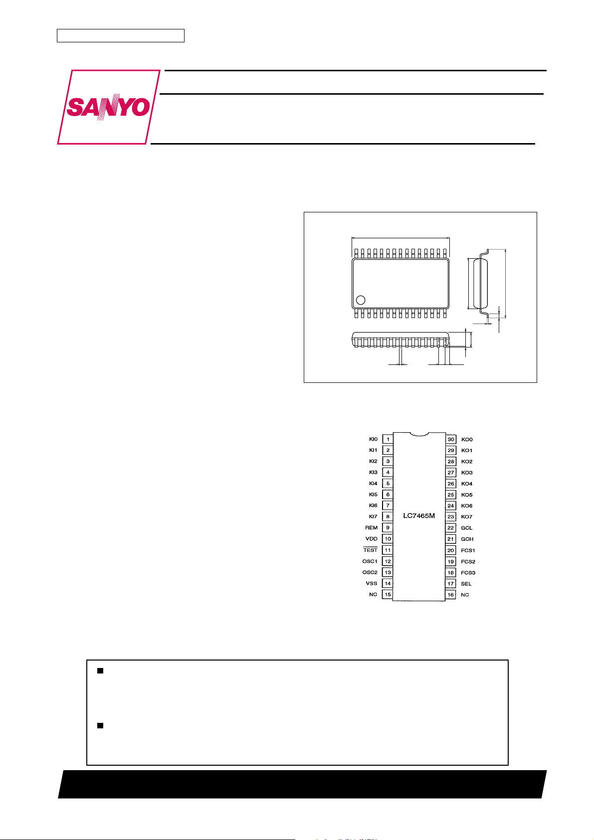
The LC7465M operates from a 2.0 to 3.6 V supply and is
available in 30-pin MFPs.
Features
• Low external component count.
• 64 function keys.
• 256 function codes.
• Mask-programmable custom and system codes.
• 64 product codes.
• Output conforms to Japan’s Association for Electric Home
Appliances recommended standards for infrared remote
controls.
• On-chip input pull-down resistors.
• 2.0 to 3.6 V supply.
• 30-pin MFP.
Package Dimensions
unit:mm
3073B-MFP30SD
[LC7465M]
15.2
30
1
0.4
Pin Assignment
16
15
(2.25)
0.1
(0.6)
1.0
SANYO : MFP30SD
7.9
0.25
2.45max
9.2
0.65
10.5
Top view
71901TN (KT)/2123JN No.3590–1/8
Page 2
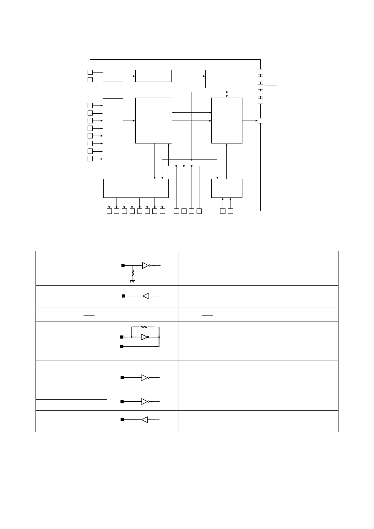
Block Diagram
LC7465M
OSC1
OSC2
Pin Description
rebmuNemaNtiucrictnelaviuqEnoitpircseD
KI0
KI1
KI2
KI3
KI4
KI5
KI6
KI7
OSC
KEY
INPUT
BUFFER
KEY DIGIT
TIMING GENERATOR
KO0
KO1
KO2
KO3
DIVIDER
KEY
DATA
REGISTER
KO4
KO5
KO6
KO7
SEL
FCS1
FCS2
FCS3
TIMING
GENERATOR
OUTPUT
CONTROL
GC CODE
REGISTER
GCL
GCH
V
DD
V
SS
TEST
NC
NC
REM
8ot17IKot0IK stupnigninnacshctiwsyeK
9MERtuptuorevirdDEL
01V
11TSET noitarepolamronrofnepotfelroHGIHdeitebdluohsTSET.tupnitseT
211CSO noitcennoctupnirotallicsocimareC
312CSO noitcennoctuptuorotallicsocimareC
41V
61,51CN nepotfelebdluohS.noitcennocoN
71LES stupnitcelesedomedocnoitcnuF
02ot813SCFot1SCF stupnitcelesedocnoitcnuF
12HCG
22LCG
03ot327OKot0OK stuptuogninnacshctiwsyeK
DD
SS
egatlovylppuS
dnuorG
stupnitcelesedoctcudorP
No.3590–2/8
Page 3
LC7465M
Specifications
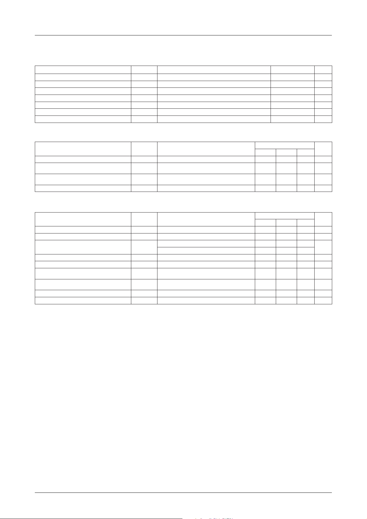
Absolute Maximum Ratings at Ta = 25˚C
retemaraPlobmySsnoitidnoCsgnitaRtinU
egatlovylppusmumixaMV
egatlovtupnIV
egatlovtuptuOV
tnerructuptuOI
noitapissidrewopelbawollAxamdP 051Wm
erutarepmetgnitarepOrpoT –58+ot04
erutarepmetegarotSgtsT –521+ot05
Recommended Operating Conditions at Ta = –40 to +85˚C
retemaraPlobmySsnoitidnoC
egnaregatlovylppuSV
LESdna3SCFot1SCF,HCG,LCG,7IKot0IK
egatlovlevel-hgihtupni
LESdna3SCFot1SCF,HCG,LCG,7IKot0IK
egatlovlevel-woltupni
ycneuqerfrotallicsOf
xamDD
I
O
O
Ta≤85˚C
DD
V
HI
V
LI
CSO
VSS–5.5+ot3.0V
VSS–Vot3.0
VSS–Vot3.0
sgnitaR
nimpytxam
0.20.36.3V
V7.0
DD
V
SS
334554
3.0+
DD
3.0+
DD
–53Am
V
DD
V3.0
DD
774
˚C
˚C
V
V
tinU
V
V
zHk
Electrical Characteristics at Ta = –40 to +85˚C, V
retemaraPlobmySsnoitidnoC
tnerrucylppusgnitarepOI
tnerrucylppusybdnatSI
tnerruclevel-hgihtuptuoMERI
egatlovlevel-hgihtuptuo7OKot0OKV
egatlovlevel-woltuptuoMERdna7OKot0OKV
level-hgihtupni3SCFot1SCFdnaHCG,LCG
tnerruc
level-woltupni3SCFot1SCFdnaHCG,LCG
tnerruc
egatlovgnitaolftupni7IKot0IKV
ecnatsisernwod-lluptupni7IKot0IKR
DD
SD
V
HO
HO
LO
I
HI
I
LI
FI
NI
DD
V
DD
IHO=– Am1.0
I
LO
VIV=
VIV=
= 2.0 to 3.6 V
DD
sgnitaR
nimpytxam
daolon,desserpyeK 1Am
deppotsrotallicso,desserpyekoN 1Aµ
V,V2=
V,V3=
Am1.0= 3.0V
DD
SS
–V1–5.2
HOV=DD
–V1–11
HOV=DD
VDD–3.0
1Aµ
–1 Aµ
V1.0
DD
57001
521
tinU
Am
V
V
kΩ
No.3590–3/8
Page 4

LC7465M
1
2
3
4
5
6
7
8
9
10
11
12
13
14
15
16
17
18
19
20
21
22
23
24
25
26
27
28
29
30
31
32
33
34
35
36
37
38
39
40
41
42
43
44
45
46
47
48
49
50
51
52
53
54
55
56
57
58
59
60
61
62
63
64
KI0 KI1 KI2 KI3 KI4 KI5 KI6 KI7
KO0
KO1
KO2
KO3
KO4
KO5
KO6
KO7
Functional Description
Key Inputs
An eight-by-eight matrix is formed with the keyswitch
scanning outputs KO0 to KO7 and the keyswitch scanning inputs KI0 to KI7 as shown in the following figure.
When a key is held down, either the normal or abbreviated continuation code is output continously, depending
on the mask option selected.
Normally, only one key can be pressed at a time. If more
than one key is pressed, all keys are ignored and no
output is generated. However, when the appropriate mask
option is selected, seven function codes can be generated
by holding down key 8 and one of keys 16, 24, 32, 40,
48, 56 and 64 as shown in table 1.
Output Data Configuration
The 48-bit output data configuration is shown in the
following figure. Note that the data is sent least-significant bit first.
Table 1. Function code generation
noitanibmocyeK
0CF1CF2CF3CF4CF5CF6CF7CF
61,8 11101001
42,8 11100101
23,8 11101101
04,8 11100011
84,8 11101011
65,8 11100111
46,8 11101111
edocnoitcnuF
C0 to C15
16-bit custom code 4-bit parity 4-bit system code 8-bit product code 8-bit function code 8-bit data check code
P0 to P3 SC0 to SC3 GC0 to GC7 FC0 to FC7 DC0 to DC7
Custom code
The 16-bit mask-programmable custom code (C0 to C15)
is a unique code registered with the Association for
Electric Home Appliances.
Parity bits
The four parity bits (P0 to P3) are used for error detection. Their value is given by the following equation.
Pn=Cn ⊕ C(n+4) ⊕ C(n+8) ⊕ (n+12)
where n=0 to 3.
System code
The four-bit system code (SC0 to SC3) is mask-programmed into the LC7465M during fabrication.
Product code
The eight-bit product code (GC0 to GC7) consists of two
mask-programmable bits and six bits that are set by
connecting each of GCL and GCH to one of KO0 to
KO7. The block diagram of the product code generator is
shown in the following figure. GC1 and GC3 are the
mask-programmable bits, shown set to zero.
No.3590–4/8
Page 5

LC7465M
Tables 2 and 3 show the relationships between GCL and
L0 to L2, and between GCH and H0 to H2, respectively.
Table 2. GCL product codes
niP
0OK 000
1OK 100
2OK 010
3OK 110
4OK 001
5OK 101
6OK 011
7OK 111
0L1L2L
detarenegedoC
Table 3. GCH product codes
niP
0OK 000
1OK 100
2OK 010
3OK 110
4OK 001
5OK 101
6OK 011
7OK 111
0H1H2H
detarenegedoC
Function code
The eight-bit function code (FC0 to FC7) is determined
by the number of the key pressed and the SEL and FCS1
to FCS3 inputs.
When SEL is LOW, bits FC3 and FC7 of the function
codes for the 64 keys are determined by FCS1 and FCS3,
respectively, as shown in tabel 4 and the following figure.
Table 4. Function code generation when SEL is LOW
1SCF2SCF3SCF
WOL
HGIH
WOL
HGIH
×
×
×
×
WOL –––0–––0
WOL –––1–––0
HGIH –––0–––1
HGIH –––1–––1
0CF1CF2CF3CF4CF5CF6CF7CF
Note
× = don’t care
− = key press code
The function codes when SEL is LOW, FCS1 is HIGH
and FCS3 is LOW are shown in the following figure. For
example, when key 23 is pressed, the generated function
code is 2EH.
edocnoitcnuF
When SEL is HIGH, the function codes for keys 1 to 32
are fixed, and bits FC3, FC6 and FC7 of the function
codes for keys 33 to 64 are determined by FCS1 to FCS3
as shown in table 5 and the following figure.
No.3590–5/8
Page 6

LC7465M
Table 5. Function code generation when SEL is HIGH
1SCF2SCF3SCF
WOLWOLWOL –––0––10
HGIHWOLWOL –––1––00
WOLHGIHWOL –––0––10
HGIHHGIHWOL –––1––10
WOLWOLHGIH –––0––01
HGIHWOLHGIH –––1––01
WOLHGIHHGIH –––0––11
HGIHHGIHHGIH –––1––11
0CF1CF2CF3CF4CF5CF6CF7CF
Note
− = key press code
The function codes when SEL is HIGH, FCS1 is HIGH, FCS2 is LOW and FCS3 is HIGH are shown in the following
figure. For example, when key 45 is pressed, the generated function code is 9CH.
edocnoitcnuF
Note that when the appropriate mask option is selected, function codes 97H, A7H, B7H, C7H, D7H, E7H and F7H can
also be generated by holding down key 8 and one of keys 16, 24, 32, 40, 48, 56 and 64.
Data check code
The eight-bit data check code (DC0 to DC7) is generated by adding the carry bits from the system code to the product
and function code bits. This code is used for error detection. The data check code is calculated using the following
equation.
DC=SC+GC0 to GC3+GC4 to GC7+FC0 to
FC3+FC4 to FC7
For example, when
SC=0H, GC=0B1H, FC=35H
DC=0H+1H+0BH+5H+3H=14H
No.3590–6/8
Page 7

Data Transmission Waveforms
Abbreviated transmission mode
Abbreviated mode detail
Normal transmission mode
LC7465M
Oscillator
The LC7465M contains a self-biased CMOS inverter that is used as an oscillator when connected to a ceramic resonator as shown in the following figure. To reduce power cunsumption, the oscillator operates only when a key is pressed.
No.3590–7/8
Page 8

T ypical Application
LC7465M
Specifications of any and all SANYO products described or contained herein stipulate the performance,
characteristics, and functions of the described products in the independent state, and are not guarantees
of the performance, characteristics, and functions of the described products as mounted in the customer's
products or equipment. To verify symptoms and states that cannot be evaluated in an independent device,
the customer should always evaluate and test devices mounted in the customer's products or equipment.
SANYO Electric Co., Ltd. strives to supply high-quality high-reliability products. However, any and all
semiconductor products fail with some probability. It is possible that these probabilistic failures could
give rise to accidents or events that could endanger human lives, that could give rise to smoke or fire,
or that could cause damage to other property. When designing equipment, adopt safety measures so
that these kinds of accidents or events cannot occur. Such measures include but are not limited to protective
circuits and error prevention circuits for safe design, redundant design, and structural design.
In the event that any or all SANYO products(including technical data,services) described or
contained herein are controlled under any of applicable local export control laws and regulations,
such products must not be exported without obtaining the export license from the authorities
concerned in accordance with the above law.
No part of this publication may be reproduced or transmitted in any form or by any means, electronic or
mechanical, including photocopying and recording, or any information storage or retrieval system,
or otherwise, without the prior written permission of SANYO Electric Co. , Ltd.
Any and all information described or contained herein are subject to change without notice due to
product/technology improvement, etc. When designing equipment, refer to the "Delivery Specification"
for the SANYO product that you intend to use.
Information (including circuit diagrams and circuit parameters) herein is for example only ; it is not
guaranteed for volume production. SANYO believes information herein is accurate and reliable, but
no guarantees are made or implied regarding its use or any infringements of intellectual property rights
or other rights of third parties.
This catalog provides information as of July, 2001. Specifications and information herein are subject to
change without notice.
No.3590–8/8
 Loading...