

Page 1
Ordering number : ENN*6733
LC7456A
CMOS IC
LC7456A
U.S. Closed Caption Signal Extraction IC
Preliminary
Overview
The LC7456A receives the composite video signal from the V / C (Video Chroma) signal processor and extracts the
closed caption data. This data and a clock signal, generated by an on-chip PLL, are then sent to the decoder IC. The
LC7456A is a CMOS version of the LA7945 IC also currently in production. The differences between the LA7945 and
the LC7456A are a change from Bipolar to CMOS technology, a smaller package size (22 pins to 16 pins), and a
reduction in the external circuitry requierd.
An LC8640XX series microcontroller is needed to perform the decoding after the LC7456A has extracted the caption
data from the composite video signal.
Features
• Low power consumption due to CMOS process
• Accurate caption signal extraction using a built-in pead hold circuit and digital technology.
• Power Requirement : 5V ± 10 %
• Package : DIP16
Ver. 1.02B
21594
Any and all SANYO products described or contained herein do not have specifications that can handle
applications that require extremely high levels of reliability, such as life-support systems, aircraft's
control systems, or other applications whose failure can be reasonably expected to result in serious
physical and/or material damage. Consult with your SANYO representative nearest you before using
any SANYO products described or contained herein in such applications.
SANYO assumes no responsibility for equipment failures that result from using products at values that
exceed, even momentarily, rated values (such as maximum ratings, operating condition ranges, or other
parameters) listed in products specifications of any and all SANYO products described or contained
herein.
SANYO Electric Co.,Ltd. Semiconductor Company
TOKYO OFFICE Tokyo Bldg., 1-10, 1 Chome, Ueno, Taito-ku, TOKYO, 110-8534 JAPAN
D2000 RM (IM) O
No.6733-1/6
Page 2
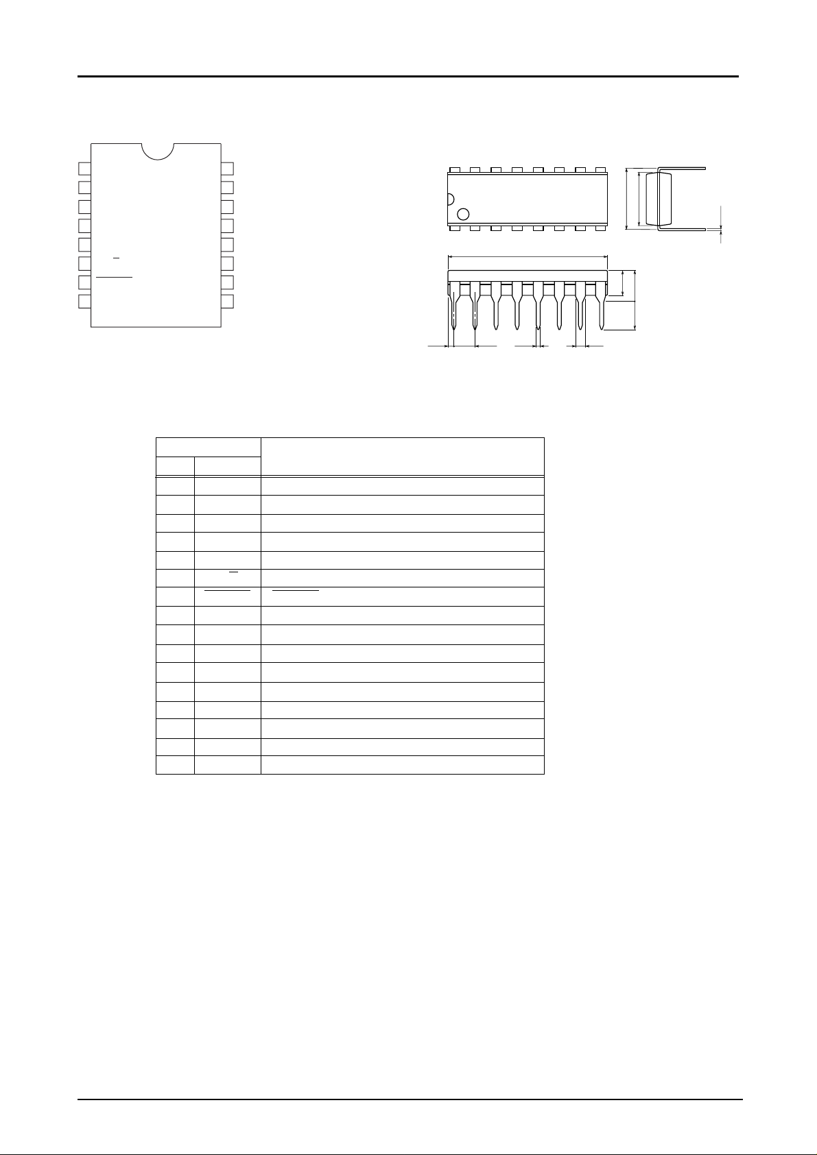
LC7456A
1
2
3
4
5
6
7
8
16
15
14
13
12
11
10
9
CP
VSS2
VDD2
TEST2
V
COR
CVIN
PEAK
SLICE
VSS1
TEST1
LN21
CPDT
CPCK
VDD1
O / E
HSYNC
ILC00006
Pin Arrangement Diagram (DIP16)
Pin Function
Pin
No. Name
1VSS1 GND
2 TEST1 Test pin, usually open
3 LN21 Line 21H pulse output
4 CPDT Caption data output
5 CPCK Caption data latch clock output
6 O/E Field determination output
7 HSYNC HSYNC input
8VDD1 Power supply
9 SILCE Caption data slice level output
10 PEAK Caption data peak hold level output
11 CVIN Composite video input
12 VCOR Built-in VCO frequency control pin
13 TEST2 Test pin, usually open
14 VDD2 Power supply
15 VSS2 GND
16 CP Built-in PLL filter pin
Function
Package Dimensions
unit : mm
3006B
16
1
19.2
0.71 2.54
0.48
9
6.4
7.62
8
3.0
3.65max
3.4
1.2
SANYO : DIP16(300mil)
0.25
No.6733-2/6
Page 3

System Block Diagram and Application
LC7456A
C-Video
1000pF
1MΩ
2.2µF
3.3KΩ
+
--
16 15 14 13 12 11 10 9
PLL
(VCO)
DATA PEAK HOLD
(Data Slice)
1
10KΩ
HSYNC PEAK HOLD
DATA SLICER
1µF
CLAMP
(Hsync Slice)
8765432
LC8640XX
From
Fly Back
ILC00081
No.6733-3/6
Page 4

LC7456A
1. Absolute Maximum Ratings at V
Parameter Symbol Pins Conditions
Supply voltage VDDMAX VDD1, VDD2VDD1=VDD2 -- 0.3 +7.0 V
Input voltage V
Output voltage V
Maximum Pdmax DIP16 300 mW
power
dissipation
Operating Topr -- 30 +70 °C
temperature
range
Storage Tstg -- 55 +150
temperature
range
* VSS1 and VSS2 are same level.
VDD1 and VDD2 are also same level.
I
O
HSYNC, CVIN -- 0.3 VDD+0.3
LN21, CPDT -- 0.3 VDD+0.3
CPCK, O / E
2. Recommended Operating Range at V
Parameter Symbol Pins Conditions
Operating V
supply voltage
Input high V
voltage
Input low V
voltage
CVIN analog CVSYNC C
input range
HSYNC input fH HSYNC 4.5 to 5.5 15.60 15.73 15.90 KHz
frequency range
DD
IH
IL
VDD1,VDD2VDD1=VDD2 4.5 5.5 V
HSYNC 4.5 to 5.5 0.85V
HSYNC 4.5 to 5.5 V
VIN
=0V and Ta=25°C
SS
=0V and Ta= -- 30°C to +70°C
SS
SYNC-WHITE=1.0V
Ratings
min. typ. max.
Ratings
VDD[V] min. typ. max.
V
DD
0.25V
1Vp-p+3dB
4.5 to 5.5
DD
SS
1Vp-p-3dB
1Vp-p
unit
unit
DD
3. Electrical Characteristics at V
Parameter Symbol Pins Conditions
Input high I
current
Input low I
current
Output high V
voltage CPCK, O / E
Output low V
voltage CPCK, O / E
Input clamp VCLMP C
voltage
IH
IL
OH
OL
HSYNC VIN=V
HSYNC VIN=V
LN21, CPDT IOH= -- 4mA 4.5 to 5.5 VDD-1.2 V
LN21, CPDT IOL=10mA 4.5 to 5.5 1
VIN
=0V and Ta= -- 30°C to +70°C
SS
DD
SS
Ratings
VDD[V] min. typ. max.
4.5 to 5.5 1 µA
4.5 to 5.5 -- 1
5.0 2.3 2.5 2.7
unit
No.6733-4/6
Page 5

LC7456A
Parameter Symbol Pins Conditions
Clamp input CII C
VIN
C
VIN
VDD[V] min. typ. max.
=3V 5.0 5 10 18 µA
Ratings
current
Clamp output COI C
VIN
C
=2V 5.0 -- 120 -- 70 -- 30
VIN
current
Current I
DD
VDD1,VDD2 4.5 to 5.5 6 15.0 mA
dissipation
* VDD1 and VSS1 are the power pins for the digital circuits of the LC7456A, and VDD2 and VSS2 for the
analog circuits. Connect like the following figure to reduce into the both circuits.
LC7456A
Power
Supply
VDD1
VSS1
VDD2
VSS2
ILC00022
unit
No.6733-5/6
Page 6

LC7456A
Specifications of any and all SANYO products described or contained herein stipulate the performance,
characteristics, and functions of the described products in the independent state, and are not guarantees
of the performance, characteristics, and functions of the described products as mounted in the customer's
products or equipment. To verify symptoms and states that cannot be evaluated in an independent device,
the customer should always evaluate and test devices mounted in the customer's products or equipment.
SANYO Electric Co., Ltd. strives to supply high-quality high-reliability products. However, any and all
semiconductor products fail with some probability. It is possible that these probabilistic failures could
give rise to accidents or events that could endanger human lives, that could give rise to smoke or fire,
or that could cause damage to other property. When designing equipment, adopt safety measures so
that these kinds of accidents or events cannot occur. Such measures include but are not limited to protective
circuits and error prevention circuits for safe design, redundant design, and structural design.
In the event that any or all SANYO products(including technical data,services) described or
contained herein are controlled under any of applicable local export control laws and regulations,
such products must not be exported without obtaining the export license from the authorities
concerned in accordance with the above law.
No part of this publication may be reproduced or transmitted in any form or by any means, electronic or
mechanical, including photocopying and recording, or any information storage or retrieval system,
or otherwise, without the prior written permission of SANYO Electric Co. , Ltd.
Any and all information described or contained herein are subject to change without notice due to
product/technology improvement, etc. When designing equipment, refer to the "Delivery Specification"
for the SANYO product that you intend to use.
Information (including circuit diagrams and circuit parameters) herein is for example only ; it is not
guaranteed for volume production. SANYO believes information herein is accurate and reliable, but
no guarantees are made or implied regarding its use or any infringements of intellectual property rights
or other rights of third parties.
This catalog provides information as of December, 2000. Specifications and information herein are subject to
change without notice.
PS
No.6733-6/6
 Loading...