

Page 1

Ordering number : ENN5680A
LC7455A/M
U.S. Closed Caption Signal Extraction IC
Overview
The LC7455A/M receives the composite video signal from V/C (Video Chroma) signal processor and extracts the closed
caption data with several signals from the decoder IC or microcomputer, are then sent to the decoder IC.
Features
(1) Low power consumption due to CMOS process
(2) Accurate caption signal extraction using a built-in peak hold circuit and digital technology.
(3) Power Requirement : 5V± 10%
(4) Package LC7455A : DIP16
LC7455M : MFP18
CMOS IC
Ver.1.01
N1494
D2700 RM (IM) Ohta No.5680-1/11
Page 2
LC7455A/M
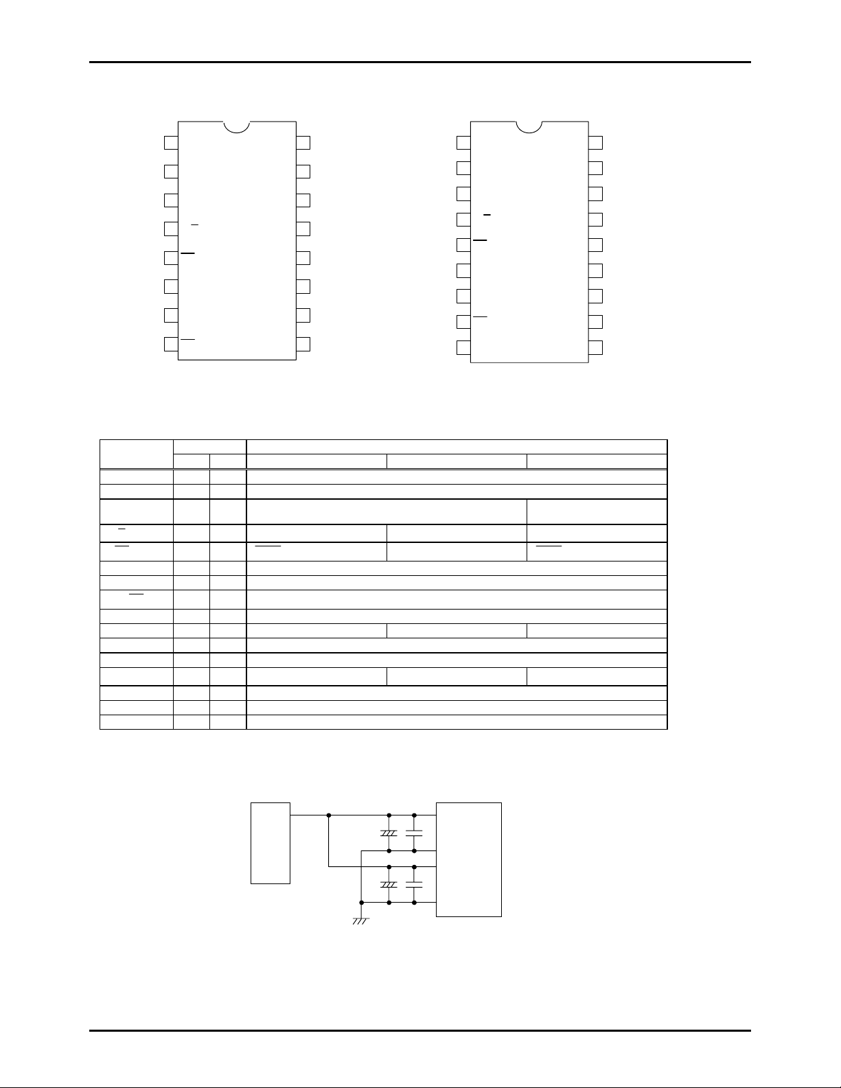
Pin Assignment
DIP16 MFP18
1
2
3
4
5
6
7
8
9
VSS1
TEST
LN21
O/
/CFOUT
E
/CFIN
HS
CPDT
SCKIN
CE
NC
1
2
3
VSS1
TEST
LN21
CP
VSS2
VDD2
16
15
14
4
O/
/CFOUT
E
MOD1
13
/CFIN
5
6
7
HS
CPDT
SCKIN
VCOR
CVIN
MOD0
12
11
10
8
CE
VDD1
9
CP
VSS2
VDD2
MOD1
VCOR
CVIN
MOD0
VDD1
NC
18
17
16
15
14
13
12
11
10
LC7455A LC7455M
Pin Description
Terminal
VSS1 1 1
TEST 2 2
LN21 3 3
O/E/CFOUT
/CFIN
HS
CPDT 6 6
SCKIN 7 7
CE
VDD1 9 11
MOD0 10 12
CVIN 11 13
VCOR 12 14
MOD1 13 15
VDD2 14 16
VSS2 15 17
CP 16 18
* VDD1,VSS1are the power supply terminals for built-in digital circuit. And VDD2,VSS2 are the power supply terminals for
built-in analog circuit. Connect like following figure to reduce the noise influence.
Pin No Function Description
DIP16 MFP18 MODE1 MODE2 MODE3
Negative power supply for digital circuit
Test pin, Leave open in operation
4 4
5 5
8 8
Line 21H pulse output (Even field) Line 21H pulse output
Field determination output CF oscillation output terminal Field determination output
output
Hsync
Caption data output (Nch open drain)
Input for Caption-data-transmission clock
Chip select input
Positive power supply for digital circuit
leave open connect to VDD1 leave open
Composite video input
Built-in VCO frequency control
leave open leave open connect to VDD1
Positive power supply for analog circuit
Negative power supply for analog circuit
Built-in PLL filter pin
CF oscillation input terminal
(Both field)
input
Hsync
LC7455A/M
Power
supply
VDD1
VSS1
VDD2
VSS2
No.5680-2/11
Page 3
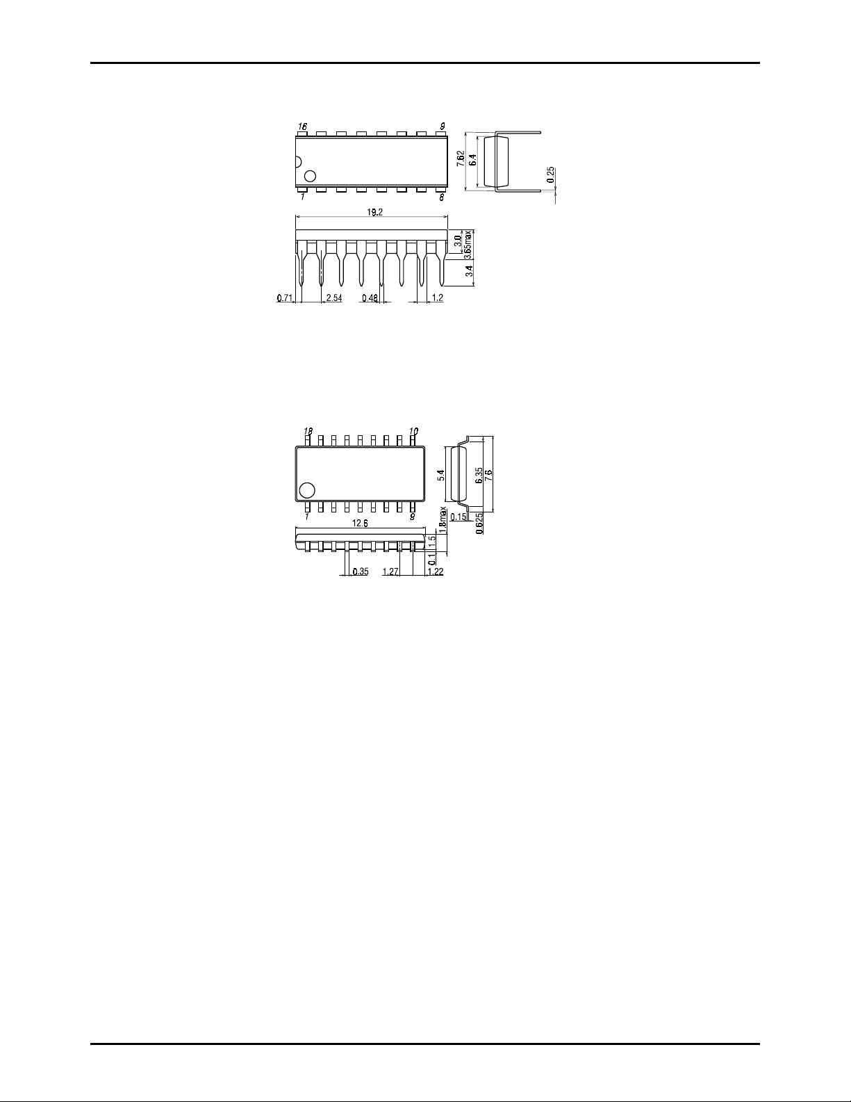
Package Dimension
(unit : mm)
3006B
(unit : mm)
3095
LC7455A/M
SANYO : DIP-16
SANYO : MFP-18
No.5680-3/11
Page 4
LC7455A/M
N
N
(
)
(
)
(
)
System Block Diagram (DIP16)
13
MOD1
16
CP
15
VSS2
14
VDD2
12
VCOR
11
CVIN
10
MOD0
VDD1
9
PLL
(VCO)
PLL
reference clock
A: MODE 2
B: MODE 3
C: MODE 1
A B C
DATA PEAK HOLD
(DATA Slice)
HSYNC
(
Hsync
CLAMP
PEAK HOLD
Slice)
DATA SLICER
Data
OUTPUT CONTROL
1
VSS
2
TEST
MODE1,3
3
LN21
O/
E
MODE2
1/32 Divider
Clock Generator
4
/CFOUT
E
O/
MODE2
5
/CFI
HS
DATA OUTPUT
BUFFER
6
CPDT
7
SCKI
8
CE
Mode Description
Terminal
MOD1 MOD0
Leave open Leave open MOD1 VTR •Extraction of Line-21 data of the even field Built-in PLL circuit uses the
Leave open Connect
to
VDD1
Connect
Leave open MOD3 NTSC-TV •Extraction of Line-21 da ta of the even/Odd field Bu ilt-in PLL circuit u ses the
to
VDD1
MODE Applications Operation
horizontal synchr on ized s ign al separ at ed from C-V ideo si gnal as the r eference of
PLL operation.
MOD2 VTR
•Extraction of Line-21 data of the even field Built-in PLL circuit uses
the 1/32-divided signal from 508KHz oscilla- tion as the reference of the
PLL operation.
Note that the 508KHz oscillation requires 508KHz-ceramic resonator externally.
horizontal synchronized signal generated fr om external Fly-Back circuit as the
reference of the PLL operation.
No.5680-4/11
Page 5
LC7455A/M
1. Absolute Maximum Ratings at VSS=0V and Ta=25°C
Parameter Symbol Pins Conditions
Supply voltage VDDMAX VDD1,VDD2 VDD1=VDD2 -0.3 - +7.0
Input voltage VI
Output voltage VIO LN21,CPDT,
dissipation
Operating
temperature
range
Storage
temperature
range
Pdmax
Topr -30 - +70
Tstg -55 - +150
HS
/CFIN,CVIN,SCKIN,
CE
E
O/
/CFOUT,
DIP16 300 Maximum power
MFP18 150
HS
/CFIN
-0.3 - VDD+0.3
-0.3 - VDD+0.3
Ratings
min. typ. max.
* VSS1 and VSS2 are same level.
* VDD1 and VDD2 are a lso same level.
2. Recommended Operating Range at Ta=-30°C to +70°C, VSS=0V
Parameter Symbol Pins Conditions
Operating
Supply voltage
Input high voltage VIH
Input low voltage VIL
CVIN input
amplitude
HS
input
frequency
range
Oscillation
frequency
range
Oscillation
stabilizing
time period
(Note 1)
(Note 2)
VDD VDD1,VDD2 VDD1=VDD2 4.5 5.5
HS
/CFIN, SCKIN,CE
HS
/CFIN, SCKIN,CE
CVSYNC CVIN SYNC-WHITE=1.0V 4.5 to 5.5
fH
FmCF
tmsCF
HS
/CFIN
HS
/CFIN, O/
/CFIN, O/E/CFOUT
HS
E
/CFOUT
Output disable 4.5 to 5.5 0.75VDD VDD
Output disable 4.5 to 5.5 VSS 0.2VDD
MODE3 4.5 to 5.5 15.23 15.73 16.23
•MODE2
•Refer to figure 1
•MODE2
•Refer to figure 2
(Note 1) The oscillation constant is shown on table 1.
(Note 2) The oscillation stable time period means the time to oscillate stably after supplyng voltage.
Ratings
VDD[V] min. typ. max.
p-p+ p-p p-p+
1V 3dB 1V 1V 3dB
4.5 to 5.5 503 508 513
4.5 to 5.5 0.5 5 ms
unit
V
mW
C
°
unit
V
kHz
No.5680-5/11
Page 6
LC7455A/M
3. Electrical Characteristics at Ta=-30°C to +70°C, VSS=0V
Parameter Symbol Pins Conditions
Input high
current
Input low
current
Output high
voltage
Output low
voltage
Input clamp
voltage
Clamp input
current
Clamp output
current
Current
dissipation
IIH
IIL
VOH LN21,CPDT,
VOL LN21,CPDT,
VCLMP CVIN 5.0 2.3 2.5 2.7
CII CVIN CVIN=3V 5.0 5
COI CVIN CVIN=2V 5.0 -120 -70 -30
IDD VDD1,VDD2 4.5 to 5.5 6 15.0 mA
/CFIN, SCKIN,
HS
CE
HS
/CFIN, SCKIN,
CE
E
O/
/CFOUT,
HS
/CFIN
O/
/CFIN,
E
HS
/CFIN
VIN=VDD 4.5 to 5.5 1
VIN=VSS 4.5 to 5.5 -1
IOH=-4mA 4.5 to 5.5 VDD-1.2
IOL=10mA 4.5 to 5.5 1
Ratings
VDD[V] min. typ. max.
4. Serial Output Characteristics at Ta=-30°C to +70°C, VSS=0V
Parameter Symbol Pins Conditions
Cycle t
Low Level
pulse width
High Level
Input clock
Serial clock
Serial output
pulse width
Set-up time
Output delay time t
CKCY
4.5 to 5.5 1
SCKIN Refer to figure 3
CKL
t
4.5 to 5.5 0.5
CKH
t
4.5 to 5.5 0.5
ICK
t
CKO
CPDT •Use test load.
•Refer to figure 3
Ratings
VDD[V] min. typ. max.
4.5 to 5.5 1
4.5 to 5.5 0.5
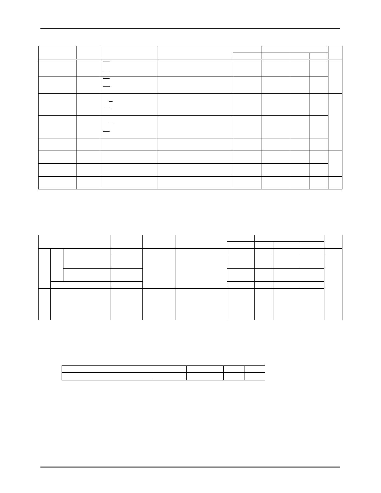
Table 1. Ceramic resonator oscillation recomm en ded constant
A kind of an oscillation Producer Oscillator C1 C2
508KHz
ceramic resonator
oscillation
* Both C1 and C2 must be use K rank (±10%) and SL characteristics.
(Notes) • Please place the oscillation-related parts as close to the oscillation pins as possible with the shortest
possible pattern length since the circuit pattern affects the oscillation frequency.
• If you use other oscillators herein, we provide no guarantee for the characteristics.
Murata CSB 508E 150pF 150pF
10
18
unit
µ
µ
unit
µ
A
V
A
s
No.5680-6/11
Page 7
Power supply
O/
/CFIN
HS
/CFOUT
E
CE
SCKIN
CPDT
state while
CE
=H
tICK
LC7455A/M
HS/CFIN O/E/CFOUT
C1 C2
CF
Figure 1 Ceramic resonator oscillation
VDD
VDD limit
0V
tmsCF
Figure 2 Oscillation stable time period
0.5VDD
<AC timing point>
tCKCY
tCKL tCKH
tCKO
<Timing> •CPDT becomes the high-inpedance
1kΩ
50pF
<Test load>
Figure 3 Serial output test condition
VDD
No.5680-7/11
Page 8

LC7455A/M
µ
µ
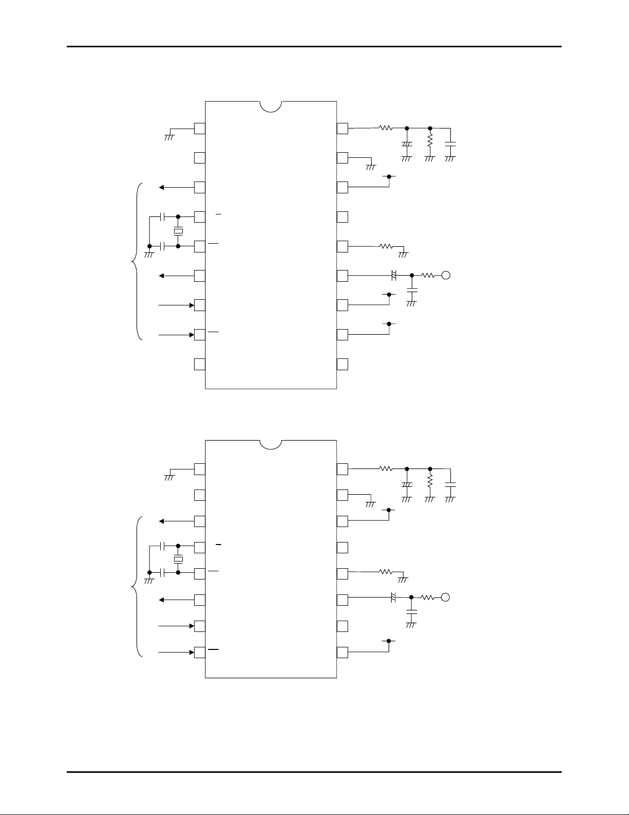
Applications (Mode 1)
MFP18
MAIN
-COM
µ
DIP16
MAIN
-COM
µ
1
2
3
4
5
6
7
8
9
1
2
3
4
5
6
7
8
VSS1
TEST
LN21
O/
/CFOUT
E
/CFIN
HS
CPDT
SCKIN
CE
NC
VSS1
TEST
LN21
/CFOUT
O/
E
/CFIN
HS
CPDT
SCKIN
CE
CP
VSS2
VDD2
MOD1
VCOR
CVIN
MOD0
VDD1
NC
CP
VSS2
VDD2
MOD1
VCOR
CVIN
MOD0
VDD1
18
17
16
15
14
13
12
11
10
16
15
14
13
12
11
10
3.3kΩ
F
+
Ω
1M
2.2
-
10kΩ
1µF
3.3kΩ
F
+
-
2.2
10kΩ
1µF
9
C-Video
Ω
1m
C-Video
1000pF
1000pF
No.5680-8/11
Page 9
LC7455A/M
CF
µ
CF
µ
Applications (Mode 2)
MFP18
MAIN
-COM
µ
DIP16
MAIN
-COM
µ
1
2
3
4
5
6
7
8
9
1
2
3
4
5
6
7
8
VSS1
TEST
LN21
O/
/CFOUT
E
/CFIN
HS
CPDT
SCKIN
CE
NC
VSS1
TEST
LN21
/CFOUT
O/
E
/CFIN
HS
CPDT
SCKIN
CE
CP
VSS2
VDD2
MOD1
VCOR
CVIN
MOD0
VDD1
NC
CP
VSS2
VDD2
MOD1
VCOR
CVIN
MOD0
VDD1
18
17
16
15
14
13
12
11
10
16
15
14
13
12
11
10
3.3kΩ
F
+
Ω
1M
-
2.2
10kΩ
1µF
3.3kΩ
F
+
-
2.2
10kΩ
1µF
9
C-Video
Ω
1M
C-Video
1000pF
1000pF
No.5680-9/11
Page 10

LC7455A/M
(
(
µ
Applications (Mode 3)
MFP18
signal
Hsync
From F.B.)
MAIN
-COM
µ
DIP16
signal
Hsync
From F.B.)
MAIN
-COM
µ
1
2
3
4
5
6
7
8
9
1
2
3
4
5
6
7
8
VSS1
TEST
LN21
O/
/CFOUT
E
/CFIN
HS
CPDT
SCKIN
CE
NC
VSS1
TEST
LN21
/CFOUT
O/
E
/CFIN
HS
CPDT
SCKIN
CE
CP
VSS2
VDD2
MOD1
VCOR
CVIN
MOD0
VDD1
NC
CP
VSS2
VDD2
MOD1
VCOR
CVIN
MOD0
VDD1
18
17
16
15
14
13
12
11
10
16
15
14
13
12
11
10
3.3kΩ
F
+
Ω
µ
1M
-
2.2
10kΩ
1µF
3.3kΩ
F
+
-
2.2
10kΩ
1µF
9
C-Video
Ω
1M
C-Video
1000pF
1000pF
No.5680-10/11
Page 11

LC7455A/M
No.5680-11/11
PS
 Loading...