

Page 1
Ordering number : ENN*6685
CMOS IC
LC7454A/M
CMOS Data Slicer
Preliminary
Overview
The LC7454A/M is a data slicer IC for the Index Plus + signals. The LC7454A/M extracts the Caption and the Index Plus +
data form the Vertical Blanking Period of the TV signal and send it out to the decoder IC (Usually Microcomputer).
The LC7454A/M can be used to extract the Closed Caption signals, the XDS signals and the Index Plus + signals.
Features
(1) Low power dessipation by CMOS process
(2) Stable signal extraction by integrated peak hold circuit and digital circuit.
(3) Operation Voltage range : 5V ± 10%
(4) Package LC7454A : DIP18
LC7454M : MFP20
Ver.1.03
90699
91400 RM (IM) Ohta No.6685-1/16
Page 2
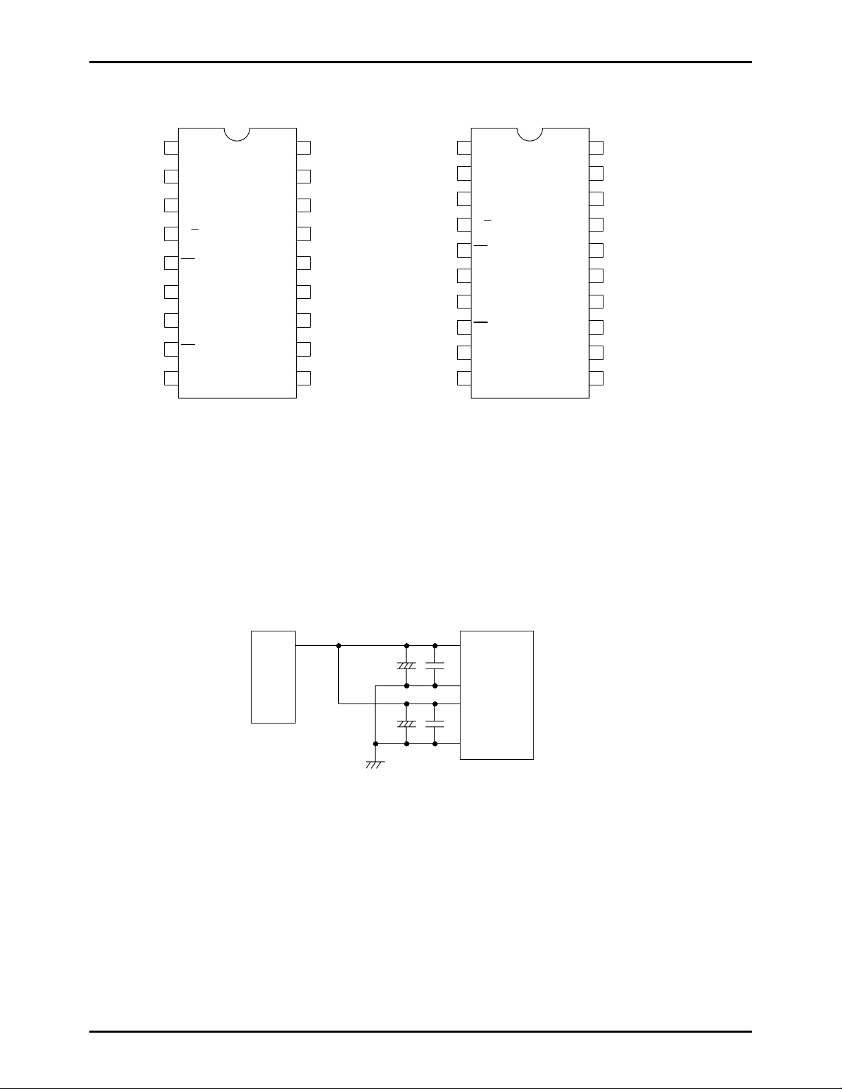
LC7454A/M
VSS
Pin Assignment
1
2
3
4
5
6
7
8
9
LC7454A LC7454M
* VDD1and VSS1are power supply terminals for digital circuit. VDD2 and VSS2 are power supply terminals for analog
circuit. Connect there terminals as the following diagram in order to reduce the noise disturbance between two powers.
DIP18 MFP20
VSS1
TEST
LN26
O/
/CFOUT
E
/CFIN
HS
DATA
SCKIN
CE
IOC
VSS2
VDD2
MOD1
VCOR
CVIN
MOD0
VDD1
SLICE
Power
supply
CP
18
17
16
15
14
13
12
11
10
1
2
3
4
5
6
7
8
9
10
VSS1
TEST
LN26
O/
/CFOUT
E
/CFIN
HS
DATA
SCKIN
CE
IOC
NC
LC7454A/M
VDD1
VSS1
VDD2
2
CP
VSS2
VDD2
MOD1
VCOR
CVIN
MOD0
VDD1
SLICE
NC
20
19
18
17
16
15
14
13
12
11
No.6685-2/16
Page 3
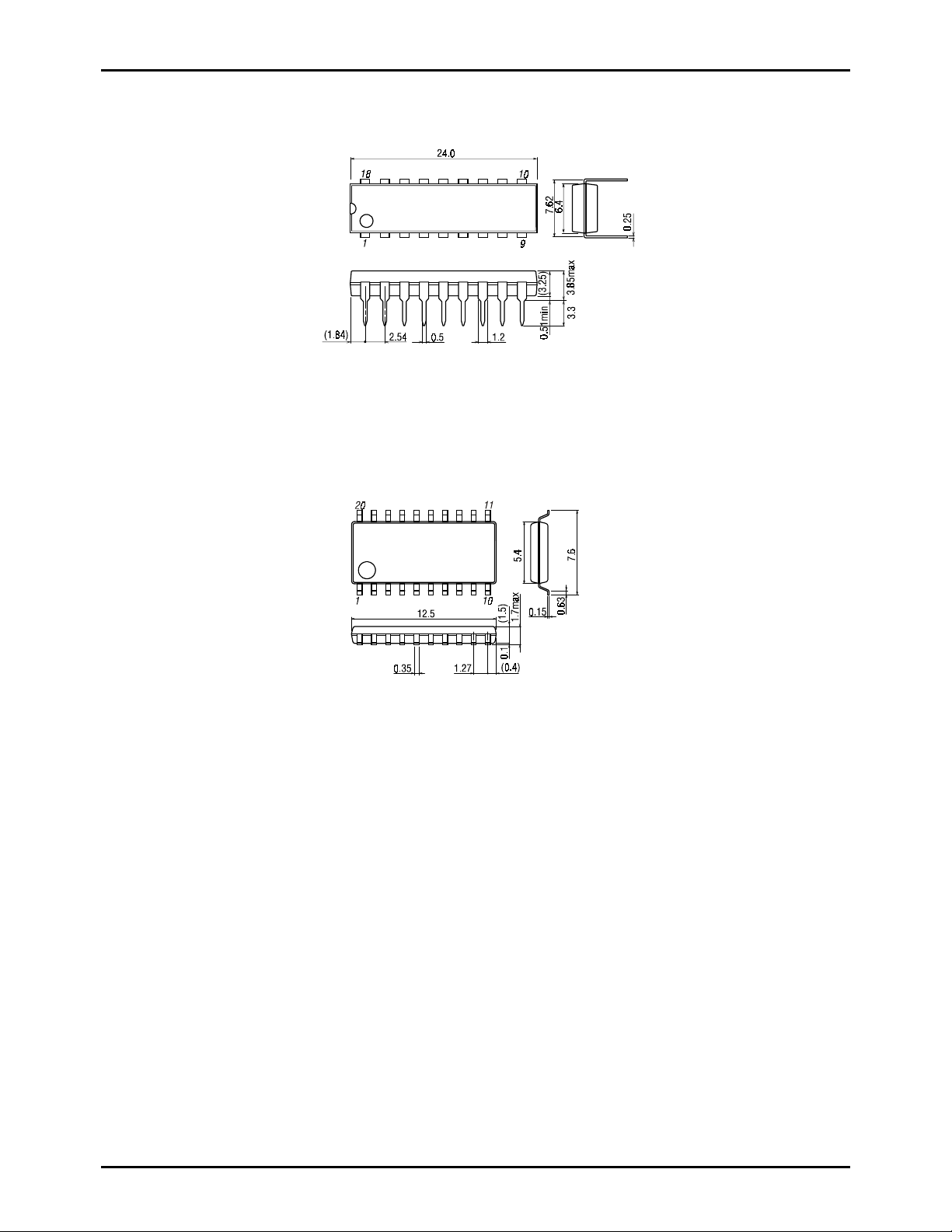
Package Dimension
(unit : mm)
3007B
Package Dimension
(unit : mm)
3036C
LC7454A/M
SANYO : DIP-18
SANYO : MFP-20
No.6685-3/16
Page 4
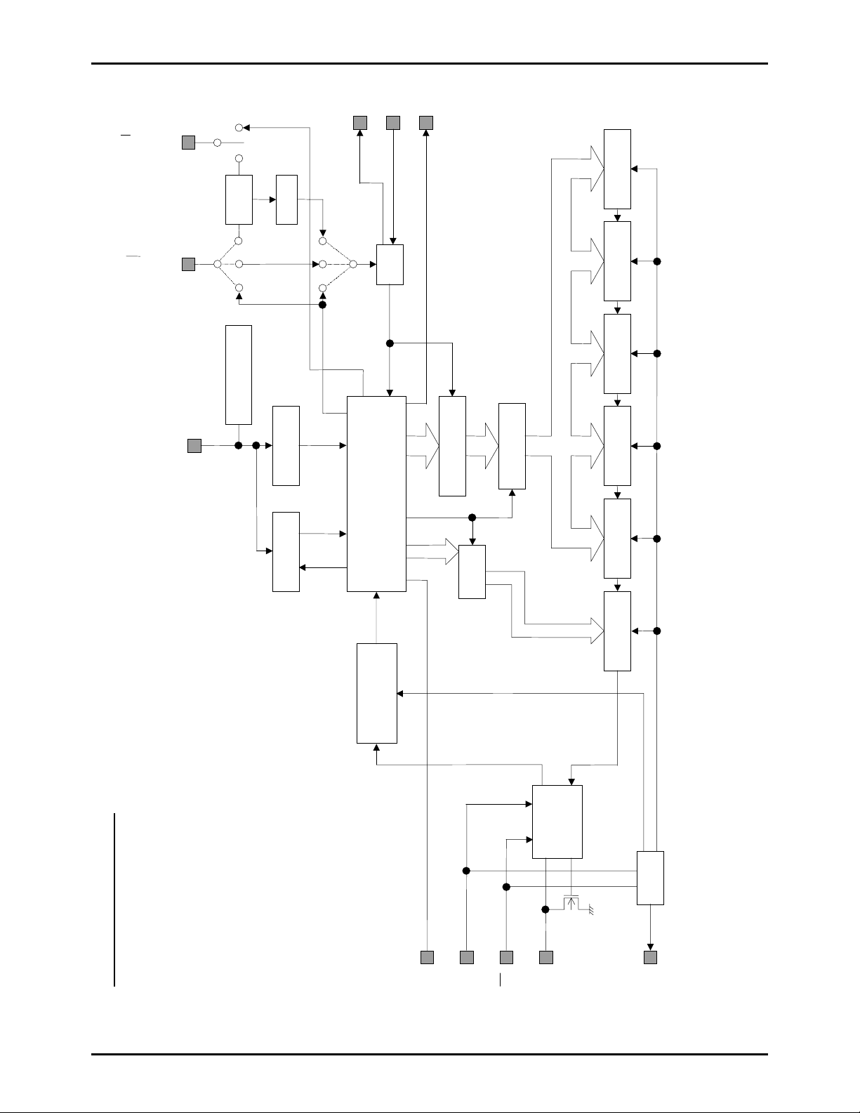
LC7454A/M
selection
li
l
CP
VCOR
SLICE
O/E/CFOUT
HS/CFIN
CVIN
(Mode 1,3)
(Mode 2)
circuit
Oscillation
(Mode 2)
(Mode3)
(Mode 1)
(Mode 2)
PLL reference clock
PLL
(Mode 3)
(Mode 1)
(VCO)
32bit data
output buffer 5
32bit data
output buffer 4
32bit data
output buffer 3
Pedestal clamp
Sync separator
control
32bit data buffer
Data transmit
32bit data
output buffer 2
cer contro
Data s
Data slicer
Slice line
data buffer
16bit line select
Data
judgment
Data
input/output
32bit data
output buffer 1
16bit data
judgement buffer
control
Input
control
LC7454system block diagram
LN26
CE
IOC
DATA
SCKIN
No.6685-4/16
Page 5
LC7454A/M
Operation on each mode
The LC7454 has three operating modes. The operation mode be selected by the status of MOD0 and MOD1 terminals. The functionality of
three modes are the same. Only the PLL reference frequen cy which is used to gener ate operat ion clo ck is di fferent. Use mod e1 or mode3
only in the application which uses 2x data. Any mode (Mode1,2 or 3) can be used in the 1x data only application.
Terminal
MOD1 MOD0
Open Open Mode1 NTSC-VCR Use H-sync signal which is separated from C-Video signal.
Open VDD1 Mode2 NTSC-VCR Use 1/32 divided signal 503 KHz which is generated by external
VDD Open Mode3 NTSC-TV Use H-sync signal from Fly Back.
Terminal Functions
Terminal #
(DIP18)
1 VSS1 Ground
2 TEST Test terminal, Open in normal operation
3 LN26 32µs Pulse output at line 26 timing on both field
4
5
6 DATA Line select data input and slice data output *2
7 SCKIN Data transmit clock input
8
9 IOC Data direction control signal input *4
10 SLICE Pulse outpu t at selected slice line
11 VDD1 Power terminal
12 MOD0 Open Connect to VDD Open
13 CVIN Conposit video input
14 VCOR Connect resister for internal VCO oscillation frequency control
15 MOD1 Open Open Connect to VDD
16 VDD2 Power terminal
17 VSS2 Ground
18 CP Filter terminal for internal PLL
*1 ‘H’ level in Odd field, ‘L’ level in Even field.
*2 N-ch open drain in output mode.
*3 Feed ‘L’ level only when data transmission is in effect. If CE=’H’, data terminal will become
input/output disable, SCKIN terminal will become input disable.
*4 ‘H’ level : Output mode
‘L’ level : Input mode
Terminal
name
O/E/CFOUT
HS
CE
MODE Applications PLL reference
ceramic resonator.
Function Description
Mode 1 Mode 2 Mode 3
Pulse output for field
judgment *1
/CFIN Sync separated HS pulse
output
Chip select input *3
Output terminal for ceramic
resonator
Input terminal for Ceramic
resonator
Pulse output for field
judgment *1
External HS pulse input
No.6685-5/16
Page 6

LC7454A/M
1. Absolute Maximum Ratings at VSS=0V and Ta=25°C
Parameter Symbol Pins Conditions
Maximum
Supply voltage
Input voltage VI CVIN,SCKIN,
Output voltage VO LN26,
Input/output
voltage
power
dissipation
Operating
temperature
Storage
temperature
VDDMAX VDD1,VDD2 VDD1=VDD2 -0.3 +7.0
-0.3 VDD+0.3
CE
,IOC
-0.3 VDD+0.3
O/
/CFOUT,SLICE
E
VIO DATA,
HS
/CFIN
Pdmax
Topr -30 +70
Tstg -55 +150
DIP18 300 Allowable
MFP20 150
-0.3 VDD+0.3
Ratings
min. typ. max.
* VSS1 and VSS2 must be the same level.
VDD1 and VDD2 must be the same level.
2. Allowable Operating Conditions at Ta=-30°C to +70°C, VSS=0V
Parameter Symbol Pins Conditions
Operating
Supply voltage
‘H’ level input
voltage
‘L’ level input
voltage
CVIN input
amplitude
input
HS
frequency
range
Oscillation
frequency
range
(Note 1)
Oscillation
stabilizing
time period
(Note 2)
VDD VDD1,VDD2 VDD1=VDD2 4.5 5.5
VIH
VIL
CVSYNC CVIN SYNC-WHITE=1.0V 4.5 to 5.5
fH
FmCF
tmsCF
/CFIN, DATA,
HS
SCKIN,
HS
SCKIN,
HS
HS
E
O/
HS
E
O/
, IOC
CE
/CFIN, DATA,
CE , IOC
/CFIN Mode3 4.5 to 5.5 15.23 15.73 16.23
/CFIN
/CFOUT
/CFIN
/CFOUT
4.5 to 5.5
4.5 to 5.5 VSS
•Mode2
•Refer to figure 1
•MODE2
•Refer to figure 2
(Note 1) Refer to table 1 for oscillator constants.
(Note 2) Oscillation stabilizing period is the time needed to stabilize the oscillation after power is fed.
Refer to
figure
2.
Ratings
VDD[V] min. typ. max.
0.75VDD
1Vp-p
-3dB
4.5 to 5.5 503
4.5 to 5.5 0.5 5 ms
VDD
0.25VDD
1V
1Vp-p
+3dB
unit
V
mW
°
C
unit
kHz
V
No.6685-6/16
Page 7

LC7454A/M
3. Electrical Characteristics at Ta=-30°C to +70°C, VSS=0V
Parameter Symbol Pins Conditions
‘H’ level input
current
‘L’ level input
current
‘H’ level
output voltage
‘L’ level
output voltage
Input clamp
voltage
Clamp input
current
Clamp output
current
Power
dissipation
IIH
IIL
VOH LN26, SLICE,
VOL LN26, DATA,
VCLMP CVIN 5.0 2.3 2.5 2.7
CII CVIN CVIN=3V 5.0 5
COI CVIN CVIN=2V 5.0 -120 -70 -30
IDD VDD1,VDD2 4.5 to 5.5 8 20 mA
/CFIN, DATA,
HS
SCKIN,
CE
HS
/CFIN, DATA,
CE
SCKIN,
E
O/
/CFOUT,
HS
/CFIN
E
/CFIN,
O/
HS
/CFIN, SLICE
VIN=VDD 4.5 to 5.5 1
, IOC
VIN=VSS 4.5 to 5.5 -1
, IOC
IOH=-4mA 4.5 to 5.5 VDD-1.2
IOL=10mA 4.5 to 5.5 1
Ratings
VDD[V] min. typ. max.
10
18
unit
µ
V
µ
4. Serial Input/Output Characteristics at Ta=-30°C to +70°C, VSS=0V
Parameter Symbol Pins Conditions
Cycle t
‘L’ Level
pulse width
‘H’ Level
Input clock
pulse width
Serial clock
Set up time
Data set up ti me t
Data hold time t
Serial input
Output delay t
Serial output
CKCY
SCKIN Refer to figure 3 4.5 to 5.5 1
CKL
t
SCKIN Refer to figure 3 4.5 to 5.5 0.5
CKH
t
SCKIN Refer to figure 3 4.5 to 5.5 0.5
ICK
SCKIN •Applied to CE
t
falling edge.
•Refer to figure 3
IDO
4.5 to 5.5 0.1
HDO
ODT
DATA •Applied to SCKIN
rising edge.
DATA •Applied to SCKIN
•Refer to figure 3
falling edge.
•Use external 1kΩ
pull-up resister.
•Refer to figure 3
Ratings
VDD[V] min. typ. max.
4.5 to 5.5 1
4.5 to 5.5 0.1
4.5 to 5.5 0.5
unit
µ
Table 1. Ceramic resonator constants
Type of oscillation Maker Resonator C1 C2
503kHz
oscillation Murata CSB 503E9 150pF 150pF
ceramic
* Both C1 and C2 must be use K rank (±10%) and SL characteristics.
(Notes) • Please place the oscillation-related parts as close to the oscillation pins as possible with the shortest
possible pattern length since the circuit pattern affects the oscillation frequency.
• If you use other oscillators herein, we provide no guarantee for the characteristics.
A
A
s
No.6685-7/16
Page 8

Power supply
O/
DATA(Output)
/CFIN
HS
/CFOUT
E
CE
SCKIN
DATA(Input)
•DATA is high-impedance when
tICK
LC7454A/M
HS/CFIN O/E/CFOUT
C1 C2
CF
Figure 1 Ceramic resonator oscillation
VDD
Lowest limit of operation
0V
tmsCF
Figure 2 Oscillation stable time period
0.5VDD
<AC timing measure point>
tCKCY
tCKL tCKH
tHDT tIDT
tODT
=H
CE
<timing>
1kΩ
50pF
<test load>
Figure 3 Serial output test condition
VDD
No.6685-8/16
Page 9

LC7454A/M
A
Slice line selection
<Input timing of slice selection data>
C-Video
Line26
LN26
CE
IOC
L level
SCKIN
DAT
D12
D11
D10 D9 D8 D7 D6 D5 D4 D3 D2 D1 D0
D13
D14
D15
Slice line selec tion d ata i s sent to the LC 745 4 in seri al for mat . When se nding the data to LC74 54, the IOC te rminal ha s to
be ‘L’ level (It will change the Data line to the input mode). The data has to be transmitted after sensing the LN26 signal.
Before sending the data, set the CE terminal to the ‘L’ level. Each bit of the data has to be changed at the falling edge of the
SCKIN and the data is captured into the LC7454 at raising edge of the SCKIN signal.
<Selection of slice line>
Maximum of 5 lines between line 10 and 25 can be selected at a time in a field. The LC7454 can slice 1x and 2x data
format signals.
Each D0 to D15 corresponds to line 10 to line 25. Set specific bit to ‘H’ to select the corresponding line.
Example: To select 15, 18, 19, 21 and 23 lines
Send D0 - D15 = [0000010011010100]
Note: If more than 6 line are selected, data extraction will be made on the first 5 lines. The data on the 6th line and after
are not extracted.
The new data sent to the LC7454 takes effects from the next field.
No.6685-9/16
Page 10

LC7454A/M
k
A
N
32 clock
40H
39H
38H
24H
23H
22H
21H
Data
32 bit data output buffer 5
20H
19H
18H
Data
Selected line 4 Selected line 3 Selected line 2 Selected line 1 Selected line 5
32 bit data output buffer 4
Data output timing
17H
Data
32 bit data output buffer 3
32 bit data output buffer 2
15H 16H
Data
37H
36H
35H
34H
33H
32H
31H
30H
29H
28H
32 clock
32 clock
32 clock
32 clock
16 clock
14H 13H
27H
b31 29 b0
b30
b1
[Data of 32 bit data output buffer 5]
b31 29 b0
b30
b1
[Data of 32 bit data output buffer 4]
b31 29 b0
b30
b1
[Data of 32 bit data output buffer 3]
b31 29 b0
b30
b1
[Data of 32 bit data output buffer 2]
b31 29 b0
b30
b1
[Data of 32 bit data output buffer 1]
b15 13 b0
b14
b1
[16 bit data judgment buffer dat a]
Data
32 bit data output buffer 1
12H
(L level)
LN26
CE
(H level)
(H level)
IOC
C-Video
26H
25H
CE
LN21
C-Video
SCKI
DAT
(inside IC)
Data transfer cloc
No.6685-10/16
Page 11

LC7454A/M
b
b
b
b
b
b
b
b
p
p
p
p
b
b
b
b
b
b
b
b
b
b
b
b
b
b
b
b
b
b
b
b
b
<Data format>
The LC7454 can extract the Index Plus + format data.
If the line contains the 1x format data, the first 15 bits of the 32 bit data buffer are filled with ‘0’ and 16th bit becomes ‘1’.
The extra cted data is stored is stored form 16th to 31st bit.
Data Byte 1
1x data format
b4 b3 b2 b1 b0
b5
Data Byte 2
p2 b6 b5 b4 b3 b2 b1 b0 p1 b6
Output
direction
LSB
0
0 0 0 0 0 0 0 0 0 0 0 0 0 0 1
b0
Fixed to ‘0000000000000001’, if 1x data is received
MSB
b4 b3 b2 b1 b0
b5
p2 b6 b5 b4 b3 b2 b1 b0 p1 b6
31
32 bit data output buffer
4
5
6
2x data format
Data Byte 2
1
0
1
2
3
Data Byte 3
2
4
5
6
0
1
2
Data Byte 4
3
3
4
5
6
0
4
1
2
3
4
5
6
Data Byte 1
0
1
2
3
Output
direction
LSB
b0
b1 b2 b3 b4 b5 b6 p1 b0 b1 b2 b3 b4 b5 b6 p2
b0
b4 b3 b2 b1 b0
b5
b3p b2 b1 b0 p3 b6
p4
b31
MSB
b6 b5 b4
32 bit data output buffer
Five 32 bit data buffer are provided to store maximum of 5 line data in a field. If the data with correct format exists in the
selected lines, the extracted data are stored into the buffers by the order of line number. If correct data is not found on the
selected line, the data buffer is filled with ‘0’. All five data buffers are cleared by the line 10 sensing signal in the next field.
Therefore, the data have to be read out between LN26 and the line 10 of the next field.
Please read only the selected buffers. For example, if three lines are selected, read the first three 32 bit buffers only.
No.6685-11/16
Page 12

LC7454A/M
b1 b
b9 b8 b7 b6 b5 b4 b3 b2 b
b0 b
b
b
b
<16 bit data judgment buffer>
The data judgment buffer includes the data which indicates the existence of the Index Plus + format data and data rate (1x
or 2x). Bit 0 to 4 contain the existence of the signal and bit 8 to 15 contain the data rate. Bit 7 contains the field information
(Odd or Even). The following table shows functions of each bit.
Output
direction
11
12
13
14
15
10
b0 to b7 : Existence of 1x or 2x data format.
Bit Contents Note
b0
b1
b2
b3
b4
b5
b6
b7
Data do not exist on the first selected line.
0 :
Data exist on the first selected line .
1 :
Data do not exist on the second selected line.
0 :
Data exist on the second selected line.
1 :
Data do not exist on the third selected line.
0 :
Data exist on the third selected line.
1 :
Data do not exist on the fourth selected line.
0 :
Data exist on the fourth selected line.
1 :
Data do not exist on the fifth selected line.
0 :
Data exist on the fifth selected line.
1 :
NOT USE
always”0”
Even field
0 :
Odd field
1 :
‘0’ if no line is selected.
‘0’ if one or less line is selected.
‘0’ if two or less line is selected.
‘0’ if three or less line is selected.
‘0’ if four or less line is selected.
b8 to b15 : Data format judgment on the selected line.
Bit Contents Note
b8
b9
b10
b11
b12
b13
b14
1x data format on the first line.
0 :
2x data format on the first line.
1 :
1x data format on the second line.
0 :
2x data format on the second line.
1 :
1x data format on the third line.
0 :
2x data format on the third line.
1 :
1x data format on the fourth line.
0 :
2x data format on the fourth line.
1 :
1x data format on the fifth line.
0 :
2x data format on the fifth line.
1 :
NOT USE
always”0”
‘0’ if no line is selected.
‘0’ if one or less line is selected.
‘0’ if two or less line is selected.
‘0’ if three or less line is selected.
‘0’ if four or less line is selected.
b15
*If neither 1x nor 2x data are sensed on the selected line, these bits become ‘0’.
*16 bit data judgment buffer is cleared at the next line 10 as well as 32 bit data output buffer 1-5.
*Even though the data judgment buffer indicates the existence of the data, it is recommended that the existence of the
data should be verified by checking the parity bit of the data.
No.6685-12/16
Page 13

LC7454A/M
µ
µ
µ
Applications (Mode 1)
DIP18
MAIN
-COM
µ
MFP20
MAIN
COM
µ
1
2
3
4
5
6
7
8
9
1
2
3
4
5
6
7
8
9
10
VSS1
TEST
LN26
O/
/CFOUT
E
/CFIN
HS
DATA
SCKIN
CE
IOC
VSS1
TEST
LN26
/CFOUT
O/
E
/CFIN
HS
DATA
SCKIN
CE
IOC
NC
CP
VSS2
VDD2
MOD1
VCOR
CVIN
MOD0
VDD1
SLICE
CP
VSS2
VDD2
MOD1
VCOR
CVIN
MOD0
VDD1
SLICE
NC
18
17
16
15
14
13
12
11
10
20
19
18
17
16
15
14
13
12
11
10kΩ
10kΩ
1
1µF
F
+
Ω
-
1M
2.2
C-Video
F
F
Ω
+
1M
-
2.2
C-Video
No.6685-13/16
Page 14
LC7454A/M
µ
Applications (Mode 2)
DIP18
MAIN
-COM
µ
1
2
3
4
5
6
7
8
9
VSS1
TEST
LN26
O/
/CFOUT
E
/CFIN
HS
DATA
SCKIN
CE
IOC
CP
VSS2
VDD2
MOD1
VCOR
CVIN
MOD0
VDD1
SLICE
18
17
16
15
14
13
12
11
10
10kΩ
+
F
Ω
µ
-
1M
2.2
C-Video
F
1
MFP20
1
2
3
VSS1
TEST
LN26
CP
VSS2
VDD2
20
19
18
F
µ
2.2
Ω
+
1M
-
4
/CFOUT
O/
CF
E
5
/CFIN
HS
6
7
DATA
SCKIN
MOD1
VCOR
CVIN
MOD0
17
16
15
14
10kΩ
C-Video
1µF
8
MAIN
-COM
µ
CE
9
IOC
VDD1
SLICE
13
12
10
NC
NC
11
No.6685-14/16
Page 15

LC7454A/M
µ
(
Applications (Mode 3)
DIP18
signal
Hsync
From F.B.)
MAIN
-COM
µ
1
2
3
4
5
6
7
8
9
VSS1
TEST
LN26
/CFOUT
O/
E
/CFIN
HS
DATA
SCKIN
CE
IOC
CP
VSS2
VDD2
MOD1
VCOR
CVIN
MOD0
VDD1
SLICE
18
17
16
15
14
13
12
11
10
10kΩ
1µF
F
2.2
+
-
C-Video
Ω
1M
MFP20
signal
Hsync
(From F.B.)
MAIN
-COM
µ
1
2
3
4
5
6
7
8
9
10
VSS1
TEST
LN26
/CFOUT
O/
E
/CFIN
HS
DATA
SCKIN
CE
IOC
NC
CP
VSS2
VDD2
MOD1
VCOR
CVIN
MOD0
VDD1
SLICE
NC
20
19
18
17
16
15
14
13
12
11
10kΩ
1µF
F
µ
2.2
+
-
C-Video
No.6685-15/16
Page 16

memo:
LC7454A/M
No.6685-16/16
PS
 Loading...