

Page 1

Any and all SANYO products described or contained herein do not have specifications that can handle
applications that require extremely high levels of reliability, such as life-support systems, aircraft’s
control systems, or other applications whose failure can be reasonably expected to result in serious
physical and/or material damage. Consult with your SANYO representative nearest you before using
any SANYO products described or contained herein in such applications.
SANYO assumes no responsibility for equipment failures that result from using products at values that
exceed, even momentarily, rated values (such as maximum ratings, operating condition ranges,or other
parameters) listed in products specifications of any and all SANYO products described or contained
herein.
CMOS IC
Picture-in-picture Controller for TVs and VCRs
Ordering number:ENN*3941B
LC7441N, 7441NE
SANYO Electric Co.,Ltd. Semiconductor Company
TOKYO OFFICE Tokyo Bldg., 1-10, 1 Chome, Ueno, T aito-ku, TOKYO, 110-8534 JAPAN
Preliminary
Overview
The LC7441N, 7441NE are picture-in picture (PIP) system controller ICs for use in NTSC, PAL or multi-system
(both NTSC and PAL) TVs and VCRs. The LC7441 PIP
system configuration requires discrete LC7480 A/D converter and memory ICs.
The LC7441 system controller IC provides nested-picture
main-screen/sub-screen video signal control. Single or multiple (2) sub-screens occupying 11.11% (one-third height,
one-third width) of the main-screen can be constructed and
controlled. Features include still/active display, white/color
frame, fixed/variable (screen) positioning, and wipe function for gradual sub-screen display and erasure. Sub-screen
horizontal resolution is achieved by 248 6-bit, 64-level
samples.
The LC7441 construction includes A/D interface,
vertical(VERT) filter, memory controller, odd-field decision circuits, read/write PLLs and D/A converters.
The LC7441 operates from a 5 V supply and is a v ailable in
64-pin DIPs and 64-pin QIPs.
Features
• NTSC, PAL and multi-system compatibility.
• TV and VCR signals.
• Forms component-based PIP controller system.
• One or two (nested) sub-screens occupying 11.11% of
main-screen.
• Still and active video display control.
• White and colored screen frames.
• Fixed and variable screen positioning.
• Gradual sub-screen display and erasure (wipe) function.
• A/D interface, vertical (VERT) filter , memory controller.
• Three D/A converters.
• 5 V supply.
• 64-pin DIP and 64-pin QIP.
Package Dimensions
unit:mm
3071-DIP64S
[LC7441N]
57.2
0.95 0.48 1.78 1.01
unit:mm
3159-QIP64E
[LC7441NE]
17.2
14.0
0.8
0.35
15.6
17.2
1.6
14.0
1.0
48
1.0
49
0.8
64
1.0
1
3364
321
1.6
1.0
33
32
17
16
0.8
16.8
19.05
4.0
5.0max
3.2
0.51min
SANYO : DIP64S
0.15
0.1
3.0max
2.7
SANYO : QIP64E
0.25
O3101TN (KT)/51595TH(ID)/4212JN No.3941–1/20
Page 2
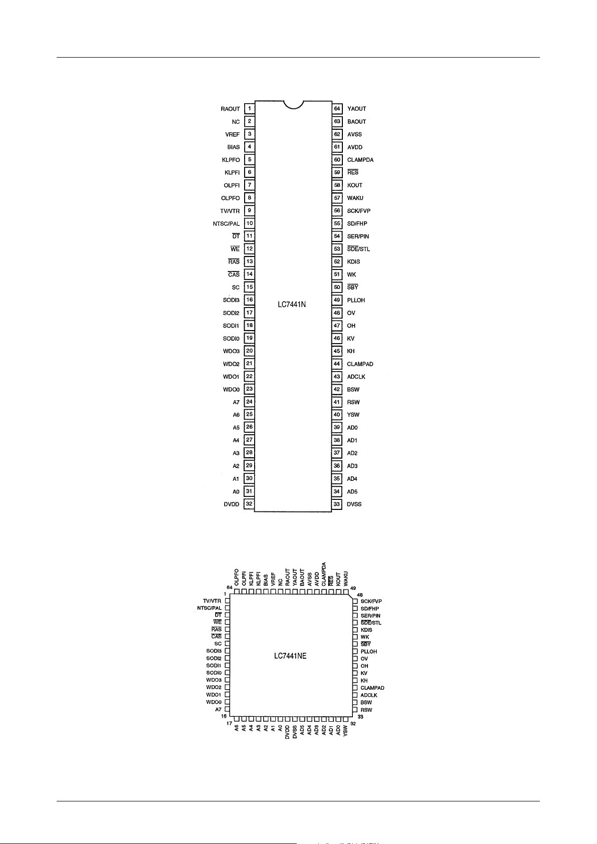
Pin Assignments
LC7441N, 7441NE
Top view
No.3941–2/20
Page 3
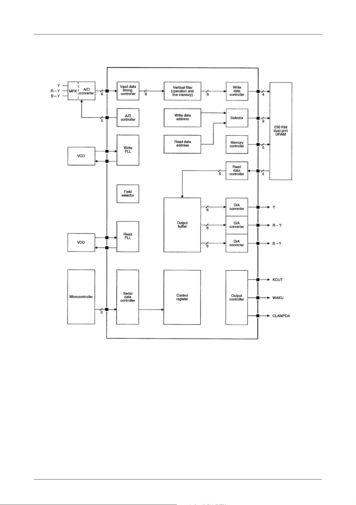
Block Diagram
LC7441N, 7441NE
No.3941–3/20
Page 4
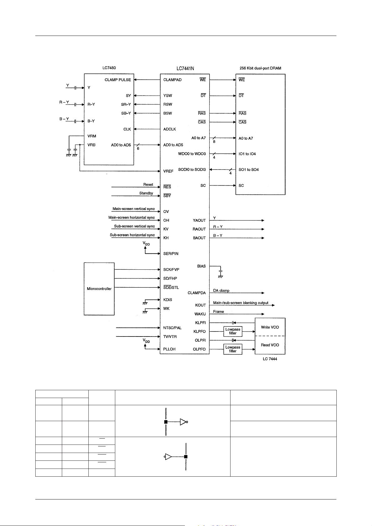
PIP System Diagram
LC7441N, 7441NE
Pin Functions
rebmuN
PIQPID
19 RCV/VT tupniSOMC,tcelesRCV/VT
201LAP/CSTN tupniSOMC,tcelesLAP/CSTN
311TD
421EW
531SAR
641SAC
751CS
emaNtiucrictnelaviuqEnoitcnuF
stuptuolortnocyromemtrop-lauD
Continued on next page.
No.3941–4/20
Page 5
LC7441N, 7441NE
Continued from preceding page.
rebmuN
PIQPID
8613IDOS
9712IDOS
01811IDOS
11910IDOS
21023ODW
31122ODW
41221ODW
51320ODW
61427A
71526A
81625A
91724A
02823A
12922A
22031A
32130A
4223VD
5233VD
62435DA
72534DA
82633DA
92732DA
03831DA
13930DA
2304WSY tuptuotceles-YecafretniD/A
3314WSR tuptuotcelesY–RecafretniD/A
4324WSB tuptuotcelesY–BecafretniD/A
5334KLCDA tuptuokcolc-gnilpmaS
6344DAPMALC tuptuoesluppmalcnoisrevnocD/A
7354HK tupnicnyslatnozirohneercs-buS
emaNtiucrictnelaviuqEnoitcnuF
DD
SS
stupni
LTT,atadtuptuolairesyromemtrop-laud,tib-4
seniltuptuoatadtupniyromemtrop-laud,tib-4
seniltuptuosserddayromemtrop-laud,tib-8
0A,bslehtdna,7AsibsmehT
ylppuslatigidV5
dnuorglatigiD
stupniLTTatadlatigiddelpmas,tib-6
0DA,bslehtdna,5DAsibsmehT
8364VK tupnireggirt-ttimhcS,cnyslacitrevneercs-buS
9374HO tupnicnyslatnozirohneercs-niaM
0484VO tupnireggirt-ttimhcS,cnyslacitrevneercs-niaM
1494HOLLP tupniSOMC,tceleslangiscnyslatnozirohLLP-daeR
2405YBS tupniSOMC,tesedomybdnatsWOL-evitcA
3415KW tupniSOMC,tcelesFFO/NOemarfneercs-buS
4425SIDK tupniSOMC,tcelesFFO/NOyalpsidneercs-buS
Continued on next page.
No.3941–5/20
Page 6
LC7441N, 7441NE
Continued from preceding page.
rebmuN
PIQPID
5435LTS/EDS
6445NIP/RES tupniSOMC,tcelesatadnipdnaatadlaireS
7455PHF/DS
emaNtiucrictnelaviuqEnoitcnuF
tupni
SOMC,tceleserutcipllitsdnaelbaneatadlaireS
noitisoplatnozirohneercs-busdnaatadlaireS
tupniSOMC,tceles
8465PVF/KCS
9475UKAW tuptuoemarF
0585TUOK
1595SER tupniSOMC,teserWOL-evitcA
2506ADPMALC tuptuoeslup-pmalcretrevnocA/D
3516VA
4526VA
5536TUOAB tuptuoretrevnocA/DY–B
6546TUOAY tuptuoretrevnocA/DY
751 TUOAR tuptuoretrevnocA/DY–R
852CN noitcennocoN
953 FERV tupniegatlovecnerefersretrevnocA/D
DD
SS
tupniSOMC,tceles
noitisoplacitrevneercs-busdnakcolcatadlaireS
langisgniknalb,hctiwsneercs-bus/neercs-niaM
tuptuo
ylppusgolanaV5
dnuorggolanA
064 SAIB noitcennocroticapacsaibsretrevnocA/D
165 OFPLK
266 IFPLK tupnikcolcOCVLLPcnyslatnozirohneercs-buS
367 IFPLO tupnikcolcOCVLLPcnyslatnozirohneercs-buS
468 OFPLO
tuptuoetatsirt
,pmup-egrahcLLPcnyslatnozirohneercs-buS
,pmup-egrahcLLPcnyslatnozirohneercs-niaM
tuptuoetatsirt
No.3941–6/20
Page 7

LC7441N, 7441NE
Specifications
Absolute Maximum Ratings at VDD = DVDD = AVDD, VSS = DVSS = AVSS = 0V
retemaraPlobmySsnoitidnoCsgnitaRtinU
egatlovylppuSV
egatlovtupnIV
egatlovtuptuOV
noitapissidrewopelbawollAxamdP 005Wm
erutarepmetgnitarepOrpoT –07+ot01
erutarepmetegarotSgtsT –521+ot55
DD
I
O
–0.7+ot3.0V
Vot3.0
3.0+
–
–
DD
Vot3.0
DD
V
3.0+
V
˚C
˚C
Allowable Operating Ranges at Ta = 25˚C, VDD = DVDD = AV
retemaraPlobmySsnoitidnoCsgnitaRtinU
egatlovylppuSV
egnaregatlovylppuSV
DD
DD
DD
Electrical Characteristics at Ta = 23 to 27˚C, VDD = DVDD = AVDD = 5V ±10%, VSS = 0V
retemaraPlobmySsnoitidnoC
V
V=
HK
V=
HK
V=
Am4=
Am1=
V=
YBS
YBS
YBS
V
roDD
YBS
V=DDf,VOf=
f,zHk51=
V=DDf,VOf=
f,zHk51=
V=
SS
SS
V=
SS
IFPLK
IFPLK
tnerrucylppuslatigiDI
tnerrucylppusgolanAI
tnerrucylppusybdnatSI
tnerrucegakaeltupnII
egatlovlevel-woltupniLTTV
egatlovlevel-woltupniSOMCV
egatlovlevel-hgihtupniLTTV
egatlovlevel-hgihtupniSOMCV
egatlovecnerefeRV
egatlovtupniIFPLOdnaIFPLKV
tnerrucegakaeltuptuoOFPLOdnaOFPLKI
tpecxestuptuollarofegatlovlevel-woltuptuO
OFPLOdnaOFPLK
egatlovlevel-woltuptuoOFPLOdnaOFPLKV
tpecxestuptuollarofegatlovlevel-hgihtuptuO
OFPLOdnaOFPLK
egatlovlevel-hgihtuptuoOFPLOdnaOFPLKV
tnerrucpu-llupIFPLOdnaIFPLKI
tuptuoTUOABdnaTUOAR,TUOAY
ecnadepmi
ecnaticapacgnitasnepmocesahPC
DDD
ADD
ODD
FFO
1LI
2LI
1HI
2HI
FER
I
ZO
V
1LO
2LO
V
1HO
2HO
VP
R
AD
SB
SER
fHOf=
V
SER
fHOf=
V
SER
VI=V
I
LO
I
LO
IHO=– Am8.04.2V
IHO=– Am1V
V
SER
,zH06=
VK
f=
VK
f=
zHM02=
IFPLO
,zH06=
zHM02=
IFPLO
gnilpuoceviticapac,evaweniszHM221p-pV
nimpytxam
V7.0
–1.010.0+
DD
5V
5.5ot5.4V
sgnitaR
02Am
02Am
–
1
V3.0
2.2V
DD
1
–
1
VADD–
05Aµ
051
1Fµ
VA
tinU
01
Aµ
1+Aµ
6.0V
V
DD
V
V
DD
1.0+
Aµ
4.0
V
1
V
V
Ω
No.3941–7/20
Page 8

LC7441N, 7441NE
Timing Characteristics at Ta = 23 to 27˚C, VDD = DVDD = AVDD = 5V ±10%, VSS = 0V
retemaraPlobmySsnoitidnoC
htdiweslupVOdnaVKt
emitesirVOdnaVKt
emitllafVOdnaVKt
htdiweslupHOdnaHKt
emitesirHOdnaHKt
emitllafHOdnaHKt
htdiweslupKCSt
emitesirKCSt
emitllafKCSt
doirepKCSt
emitputesKCSotDSt
emitdlohDSotKCSt
htdiweslupEDSt
emitesirEDSt
emitllafEDSt
emitputesKCSotEDSt
emitdlohEDSotKCSt
VCR Sync Pulse
WV
RV
FV
WH
RH
FH
WCS
RCS
FCS
ICS
USD
HO
WC
RC
FC
USC
HC
sgnitaR
nimpytxam
1sµ
1sµ
002sn
05
05sn
2sµ
001sn
03sn
002sn
05sn
05sn
002sn
002sn
05sn
05
05sn
05
tinU
sn
sn
sn
Televison Sync Pulse
Serial Intreface
No.3941–8/20
Page 9

LC7441N, 7441NE
Function Description
NTSC/PAL
NTSC/PAL should be tied HIGH for NTSC, and LOW
for PAL.
retemaraP)HGIHsiRCV/VT(noisiveleT )WOLsiRCV/VT(RCV
ytiralopcnyslacitrevdnalatnoziroH
ytiraloptuptuoretrevnocA/Dlangis-Y
emarflacitrevtuptuoUKAW
gnimit
tuptuoretrevnocA/DdnaUKAW,TUOK
ylsuoenatlumistuptuO sn825deyaledUKAWdnaTUOK
TV/VCR
TV/VCR should be tied HIGH for television mode, and
LOW for VCR mode. The differences between the two
modes are shown in the following table and figure.
Note
The shaded D/A converter outputs indicate frame data. t1=132ns, t2=396ns, t3=528ns, t4=176ns, t5=308ns, t6=352ns,
t7=220ns, t8=616ns, and t9=484ns
A/D Converter Interface
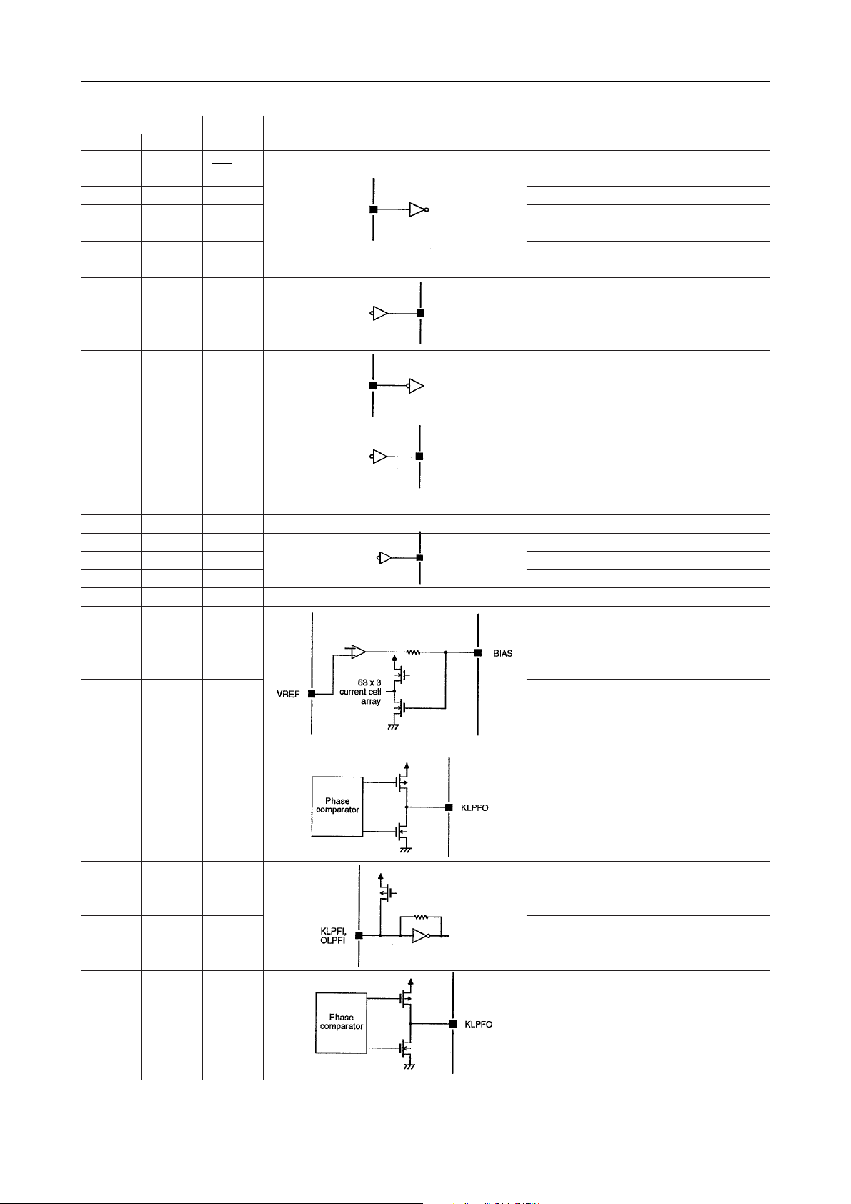
The PIP controller interfaces with an LC7480 multiplexing A/D converter using the AD0 to AD5 and VREF
R – Y, Y, B – Y, as shown in the following figure. The
conversion frequencies are shown in the following table.
inputs and CLAMPAD, YSW, RSW, BSW and ADCLK
outputs. The LC7480 converts the Y, R – Y and B – Y
video signals into 6-bit digital data which is input to the
PIP on AD0 to AD5. YSW, RSW and BSW control the
The LC7441 and LC7480 should be mounted as closely
as possible and care taken with the PCB layout because
of the high signal frequencies.
LC7480 input multiplexer. The conversion sequence is Y,
No.3941–9/20
Page 10

LC7441N, 7441NE
metsyS
f(CSTN
H
f(LAP
H
)zH437,51=530.5715.2852.1852.1
)zH526,51=000.5005.2052.1052.1
f(latoT
f023=
T
)f(Y
H
The CLAMPAD output pulse follows the KH input pulse.
CLAMPAD should be HIGH during the horizontal
blanking period as shown in the following figure.
Note
t1=5.6µs, t2=2.4µs, t3>0µs and t4>0.5µs
)zHM(ycneuqerfnoisrevnoC
f061=
YT
)f(Y–R
H
f08=H)f(Y–B
RT
Note that when KH is HIGH during reset or standby,
CLAMPAD is HIGH.
f08=H)
BT
No.3941–10/20
Page 11

LC7441N, 7441NE
On-chip D/A Converter
The normal D/A converter clock frequencies and the
clock frequencies when the RAR(Revise Aspect Ratio)
Table 1. D/A converter clock frequency
metsyS
f(CSTN
H
f(LAP
H
)zH437,51=255.7677.3677.3
)zH526,51=005.7057.3057.3
Table 2. Changing clock frequency with RAR
retsigerRARtupnILAP/CSTNYY–RY–B
WOL
HGIHWOLf614
HGIHHGIHf565
Note
× = don’t care
CLAMPDA is HIGH during main-screen horizontal sync
pulses, as shown in the following figure.
f(Y
×
f084=
YC
)f(Y–R
H
register is HIGH are shown in tables 1 and 2, respec-
tively.
)zHM(ycneuqerfkcolC
f042=
RC
f084
H
H
H
)f(Y–B
H
f042
H
f802
H
f382
H
f042=
BC
f042
H
f802
H
f382
H
)
H
The D/A converter data when the sub-screen is not
displayed are shown, msb first, in the following table.
Note that when TV/VCR is HIGH, the Y signal is output
as –Y, and when LOW, as Y.
tuptuO
TUOAY111111000000
TUOAR000001000001
TUOAB000001000001
HGIHsiRCV/VTWOLsiRCV/VT
atadretrevnocA/D
Dual-function Inputs
Input logic levels select sub-screen display parameters
when SER/PIN is LOW, and serial data and input logic
levels, when SER/PIN is HIGH, as shown in the following table.
niP
PVF/KCS
PHF/DS
LTS/EDStcelesyalpsidevitca/llitSelbaneatadlaireS
SIDKtcelesFFO/NOneercs-buS
KW
WOLHGIH
lacitrevneercs-buS
tcelesnoitisop
tcelesnoitisop
tceles
latnozirohneercs-buS
NIP/RES
kcolcatadlaireS
atadlaireS
FFO/NOneercs-buslaitinI
teser
FFO/NOemarfneercs-buS
sirellortnocnehwnoitceles
emarfneercs-buslaitinI
nehwnoitcelesFFO/NO
tesersirellortnoc
No.3941–11/20
Page 12

LC7441N, 7441NE
Serial Data Interface
When SER/PIN is HIGH, SD/FHP, SCK/FVP and SDE/
STL function as the serial-interface data, clock and dataenable inputs, respectively, as shown in the following
figure. After SDE/STL goes LOW, data bits D00 to D07
are the internal register address, and D10 to D17, the
Internal Registers
The internal control registers are shown in the following
table. Note that the lower four bits of the address byte
sserddA
H0YBSRAVKWDLIFTUOKRAVSOPLTSRPVFRPHF
H1YBSIRP2TUOK1TUOK2LTS1LTSRPVFRPHF
H8EPIWVEPIWH5PV4PV3PV2PV1PV0PV
H9RARLUM5PH4PH3PH2PH1PH0PH
HA2KW1KW5KWY4KWY3KWY2KWY1KWY0KWY
HB2RAVKW1RAVKW5KWR4KWR3KWR2KWR1KWR0KWR
HC1SFDV0SFDV5KWB4KWB3KWB2KWB1KWB0KWB
76543210
register data. After the data has been received, the
address is automatically incremented, and D20 to D27
are the data for the next register. After SDE/STL goes
from LOW to HIGH to LOW, address selection re-
occurs.
determine the register address, and the upper four bits are
ignored.
noitisoptiB
No.3941–12/20
Page 13

LC7441N, 7441NE
Reset and Standby Modes
The controller is reset by holding RES LOW and put in
standby mode by either holding SBY LOW or setting the
SBY register HIGH. The PLLs are stopped and the
internal registers set as shown in the following table.
Note that the input levels are used to determine some
initial register values. For example, if KDIS is LOW
when RES is brought LOW, then the KOUT, KOUT1 and
KOUT2 registers are set LOW.
retsigeRteseRybdnatS
YBSWOL–
,1RAVKW,RAVKW
2RAVKW
DLIFWOL–
,1TUOK,TUOK
2TUOK
RAVSOPWOL–
2LTS,1LTS,LTSLTS/EDSLTS/EDS
RPVFPVF/KCSPVF/KCS
RPHFPHF/DSPHF/DS
IRPHGIH–
WOL–
SIDKSIDK
retsigeRteseRybdnatS
EPIWVWOL–
EPIWHWOL–
5PVot0PV––
5PHot0PH––
2KW,1KWKW–
1SFDVWOL–
0SFDVHGIH–
5KWYot0KWY––
5KWRot0KWR––
5KWBot0KWB––
RAR,LUMWOL–
Note
– Register unchanged
At power-up, hold RES LOW for several microseconds
after the power supply stabilizes as shown in the following figure. Note that S and E represent the start and the
end of PIP controller operation, respectively.
Register data can be written when the controller is in
standby mode, but memory data is lost because the PLLs
are stopped and the memory is not refreshed.
Dual-port RAM Interface
The dual-port RAM interface comprises the SODI0 to
SODI3 inputs and A0 to A7, WDO0 to WDO3, WE, DT,
RAS, CAS and SC outputs.
The LC7441 and the dual-port RAM should be mounted
as closely as possible and care taken with the PCB
layuout because of the high speed of memory accesses.
The data read, memory refresh and data transfer waveforms are shown in figures 1, 2 and 3, respectively. Note
that when RAR is HIGH, t = 1/1696fH if NTSC/PAL is
also HIGH, and t = 1248fH if NTSC/PAL is LOW.
No.3941–13/20
Page 14

LC7441N, 7441NE
Figure 1. Data read
Figure 2. CAS before RAS memory refresh
Figure 3. Data transfer
No.3941–14/20
Page 15

LC7441N, 7441NE
Memory Write Range
The horizontal memory-write range is 252 dots comprising 126, 63 and 63 dots of Y, R – Y and B – Y data,
respectively. The NTSC and PAL vertical memory-write
ranges are 80 and 85 horizontal lines, respectively, as
shown in figures 4 and 5, respectively.
Figure 4. NTSC memory write range
Figure 5. PAL memory write range
No.3941–15/20
Page 16

LC7441N, 7441NE
Memory Readout Range
The horizontal memory-readout range is 244 dots
comprising 122, 61 and 61 dots of Y, R – Y and B – Y
data, respectively. The NTSC and PAL vertical memory
readout ranges are 77 and 83 horizontal lines, respectively, as shown in figures 6 and 7, respectively.
Figure 6. NTSC memory readout range
Sync Signals
The PCB layout should not allow noise to be induced in
the OH, OV, KH and KV signals from the sync-separator
IC because this can cause screen distortion. The subscreen display should be turned off when the sync signals
Figure 7. PAL memory readout range
become unstable because the display can become distorted. The OH and KH input signals should lag the
video horizontal sync signals by 1 µs as shown in the
following figure.
Note
tW > 1 µs
PLLOH
The read-PLL locks to the main-screen horizontal sync
frequency when PLLOH is HIGH, and to the sub-screen
horizontal sync frequency, when PLLOH is LOW. Using
a PLL clock to generate the horizontal sync signal and
determine the sub-screen display position results in an
error-free display.
PLLOH is normally held HIGH. However, when OH is
unstable, PLLOH should be held LOW, otherwise the
PLL clock becomes unstable and the sub-screen flickers.
Odd-field Decision Circuits
The OH/OV and KH/KV odd-field decision circuits
measure the phase difference between the horizontal and
vertical sync pulses as shown in the following figure.
When the field is odd, a single output horizontal sync
pulse is blanked during the vertical sync pulse period,
and when even, two are blanked. The phase difference is
measured between the falling edges of the sync pulses
when TV/VCR is HIGH, and between the rising edges,
when TV/VCR is LOW.
No.3941–16/20
Page 17

LC7441N, 7441NE
Operating Information
The LC7441 operates under input pin control when SER/
PIN is LOW, and under serial control, when SER/PIN is
HIGH. It can display one sub-screen when under input
pin control, and either one or two sub-screens, when
under serial control.
Single- or Dual-screen Operation Under Serial
Control
Writing register data to address 0 selects single-screen
mode, and writing data to address 1, dual-screen mode.
The registers selecting single-screen parameters are
VWIPE, HWIPE and the address 0 registers. The register
selecting dual-screen parameters are WKVAR1,
WKVAR2 and the address 1 registers.
Sub-screen ON/OFF
Pin control
The sub-screen is ON when the KDIS input is HIGH, and
OFF, when LOW.
Serial control, single screen
The sub-screen is ON when KOUT is HIGH, and OFF,
when LOW.
Serial control, dual screen
Sub-screen 1 is ON when KOUT1 is HIGH, and OFF,
when LOW. Sub-screen 2 is ON when KOUT2 is HIGH,
and OFF, when LOW.
Sub-screen Position
The sub-screen position can be fixed or variable. The
four fixed positions are shown in figure 8, and the
variable position , which is determined by the VP0 to
VP5 and HP0 to HP5 registers as follows, in figure 9.
VP = ((VP0 to VP5) + 1) × 5H + 3H
HP= ((HP0 to HP5) + 6) ×
60f
1
H
Note that variable positions outside the main-screen area
are ignored.
Note
Figures in brackets apply to PAL displays.
Figure 9. Variable screen positions
Figure 8. Sub-screen positions
RAR
retsiger
WOLWOLf044,1
WOLHGIHf044,1
HGIHWOLf842,1
HGIHHGIHf696,1
Note
Normal write-VCO frequency is 1280fH.
LAP/CSTN
tupnI
OCV-daeR
ycneuqerf
H
H
H
H
No.3941–17/20
ycneuqerfKLC
f06
H
f06
H
f25
H
f7.07
H
Page 18

LC7441N, 7441NE
Pin control
The sub-screen position is determined by the SCK/FVP
and SD/FHP input levels as shown in the following
figure.(SCK/FVP, SD/FHP)
Serial control, single screen
The sub-screen position is variable when POSVAR is
HIGH, and fixed, when LOW. The fixed screen position
is determined by FVPR and FHPR at address 0 as shown
in the following figure.
YWK0 to YWK5, RWK0 to RWK5 and BWK0 to
BWK5 are used to set the frame color. The white frame
corresponds to YWK, RWK and BWK data values of
110000, 100000 and 100000, respectively.
Pin control
The frame, which is always white, is ON when the WK
input is HIGH, and OFF, when LOW.
Serial control, single screen
The frame is ON when the WK input is HIGH, and OFF,
whe LOW. The frame color is set using the frame-color
registers when WKVAR is HIGH, and white, when LOW.
When register FILD is HIGH, the field screen is displayed; when LOW, the frame screen is displayed.
Serial control, dual-screen
The screen 1 frame is ON when WK1 is HIGH, and OFF,
when LOW. The screen 2 frame is ON when WK2 is
HIGH, and OFF, when LOW.
Serial control, dual screen
The screen 1 position is fixed, and is determined by
FVPR and FHPR at address 1. The screen 2 position is
variable, and is determined by VP0 to VP5 and HP0 to
HP5.
Sub-screen Frame
The sub-screen, or screens, can have no frame, a white
frame or a colored frame. The D/A converter registers
EPIWVEPIWHnoitarepO
WOLWOL
HGIHWOL
The screen 1 frame color is set using the frame-color
registers when WKVAR1 is HIGH, and white, when
LOW. The screen 2 frame color is set using the framecolor registers when WKVAR2 is HIGH, and white,
when LOW.
Wipe Function
The wipe function allows gradual display or erasure of
the sub-screen when in serial control, single-screen
mode. Wipe direction is set using the VWIPE and
HWIPE registers as shown in the following table. When
wiping is OFF, the sub-screen turns ON and OFF instantaneously, otherwise screen display and erasure occurs in
64 stages over approximately one second. Note that
screen erasure is in the reverse sequence to display.
WOLHGIH
HGIHHGIH
No.3941–18/20
Page 19

LC7441N, 7441NE
Dual-screen Priority
When the dual screens overlap vertically, the priority of
screen display is determined by the PRI register. The
higher screen has priority when PRI is HIGH, and the
lower screen, when LOW as shown in the following
figure.
When the higher screen has priority, the lower screen is
OFF, and when the lower screen has priority, the higher
screen display ends at the first overlapped screen line.
Note that prioritized display occurs even if the screens do
not superimpose and that side-by-side sub-screens cannot
be displayed.
Note
The dotted areas do not display.
Multi-system Display
Multi-system mode is selected when the MUL register is
HIGH, and single-system mode, when LOW. In multisystem mode, the fixed vertical positions correspond to
the main-screen system, and in single-system mode, to
the sub-screen system, as shown in the following table.
LUM
retsiger
WOLWOLH84H891
WOLHGIHH34H851
HGIHWOLH34H851
HGIHHGIHH84H891
LAP/CSTN
tupnI
HPVLPV
No.3941–19/20
Page 20

LC7441N, 7441NE
A PAL sub-screen expands vertically in a multi-system
display and an NTSC sub-screen contracts because the
two systems use a different number of scan lines. These
changes in the sub-screen aspect ratios are corrected
using the RAR(Revise Aspect Ratio) register, as shown
in the following figure. When RAR is HIGH, the horizontal clock frequency is adjusted to correct the aspect
ratio.
Specifications of any and all SANYO products described or contained herein stipulate the performance,
characteristics, and functions of the described products in the independent state, and are not guarantees
of the performance, characteristics, and functions of the described products as mounted in the customer's
products or equipment. To verify symptoms and states that cannot be evaluated in an independent device,
the customer should always evaluate and test devices mounted in the customer's products or equipment.
SANYO Electric Co., Ltd. strives to supply high-quality high-reliability products. However, any and all
semiconductor products fail with some probability. It is possible that these probabilistic failures could
give rise to accidents or events that could endanger human lives, that could give rise to smoke or fire,
or that could cause damage to other property. When designing equipment, adopt safety measures so
that these kinds of accidents or events cannot occur. Such measures include but are not limited to protective
circuits and error prevention circuits for safe design, redundant design, and structural design.
In the event that any or all SANYO products(including technical data,services) described or
contained herein are controlled under any of applicable local export control laws and regulations,
such products must not be exported without obtaining the export license from the authorities
concerned in accordance with the above law.
No part of this publication may be reproduced or transmitted in any form or by any means, electronic or
mechanical, including photocopying and recording, or any information storage or retrieval system,
or otherwise, without the prior written permission of SANYO Electric Co. , Ltd.
Any and all information described or contained herein are subject to change without notice due to
product/technology improvement, etc. When designing equipment, refer to the "Delivery Specification"
for the SANYO product that you intend to use.
Information (including circuit diagrams and circuit parameters) herein is for example only ; it is not
guaranteed for volume production. SANYO believes information herein is accurate and reliable, but
no guarantees are made or implied regarding its use or any infringements of intellectual property rights
or other rights of third parties.
This catalog provides information as of October, 2001. Specifications and information herein are subject
to change without notice.
PS No.3941–20/20
 Loading...