

Page 1
Ordering number : EN*4872A
93098HA (OT) / 30295TH (OT) No. 4872-1/19
LC74401E, 74402, 74402E
SANYO Electric Co.,Ltd. Semiconductor Bussiness Headquarters
TOKYO OFFICE Tokyo Bldg., 1-10, 1 Chome, Ueno, Taito-ku, TOKYO, 110-8534 JAPAN
PIP Controllers
CMOS IC
Any and all SANYO products described or contained herein do not have specifications that can handle
applications that require extremely high levels of reliability, such as life-support systems, aircraft’s
control systems, or other applications whose failure can be reasonably expected to result in serious
physical and/or material damage. Consult with your SANYO representative nearest you before using
any SANYO products described or contained herein in such applications.
SANYO assumes no responsibility for equipment failures that result from using products at values that
exceed, even momentarily, rated values (such as maximum ratings, operating condition ranges, or other
parameters) listed in products specifications of any and all SANYO products described or contained
herein.
Overview
The LC74401E, LC74402, and LC74402E are memory
controllers for TV set and VCR PIP (picture in picture)
systems. Since these LSIs include three D/A converter
circuits, a component PIP system can be constructed by
combining one of these LSIs with memory and an A/D
converter such as the LC7480.
Features
• Horizontal resolution: 600 TV lines
*1
• Three D/A converters (for the Y, R-Y, and B-Y signals)
are incorporated in the PIP memory controller block.
• High image quality is supported by vertical filter
function frame memory processing*2.
•I2C bus controlled.
• Built-in PLL circuit (requires an external LPF)
• Supports NTSC, PAL, and multiple (NTSC-PAL)
formats
• External control functions (only provided by the
LC74401E)
— 8-bit D/A converter (PWM): Six pins
— General-purpose ports: Four pins
• Sub-screen specifications
— Number of sub-screens: 1-8
*2
— Display on/off and frame on/off/color switching,
wipe function
— Supports switching between fixed (4 corners) and
arbitrary (8-bit specification of vertical and
horizontal position) display positions.
— Size: Area: 1/4, 1/9, 1/16, Vertical compression: 1/2,
1/3, 1/4; Horizontal compression: 2/3, 1/3, 1/6
Note: Horizontal compression can be adjusted by
changing the PLL divisor.
The display area can be changed independently
in the vertical and horizontal directions.
— Horizontal resolution (Y signal): About 250 dots
— Gradation (quantization): 64 (6 bits)
• Operating supply voltage: 5 V ± 10%
• QFP80E: LC74401E
• DIP64S: LC74402-Pin assignment identical to the
LC7442 (except for the serial control pins)
• QFP64E: LC74402E-Pin assignment identical to the
LC7442E (except for the serial control pins)
Note 1
When the main screen synchronization PLL has the standard value
(PLL7 to PLL3 = 10011)
Note 2: The specifications depend on the amount of
external memory as listed in the table below.
o: Frame display of both dynamic and static images supported.
(Frame memory processing)
▲▲: Frame display of dynamic images only supported.
✕: Not supported.
Note: The number of sub-screens listed in the table above are doubled
in split mode. (However, image quality is reduced.)
D/A Clock
Y 15.00 MHz
R-Y 3.75 MHz
B-Y 3.75 MHz
Display memory 256 K 1 M
One screen ▲▲ o
Two screens ✕ o
Three screens ✕ ▲▲
Four screens ✕ ▲▲
Page 2

Pin Assignments
No. 4872-2/19
LC74401E, 74402, 74402E
unit: mm
3159-QFP64E
[LC74402E]
unit: mm
3071-DIP64S
SANYO: DIP64S
[LC74402]
Package Dimensions
unit: mm
3074-QFP80E
SANYO: QIP80E
[LC74401E]
SANYO: QIP64E
Page 3
No. 4872-3/19
LC74401E, 74402, 74402E
Page 4
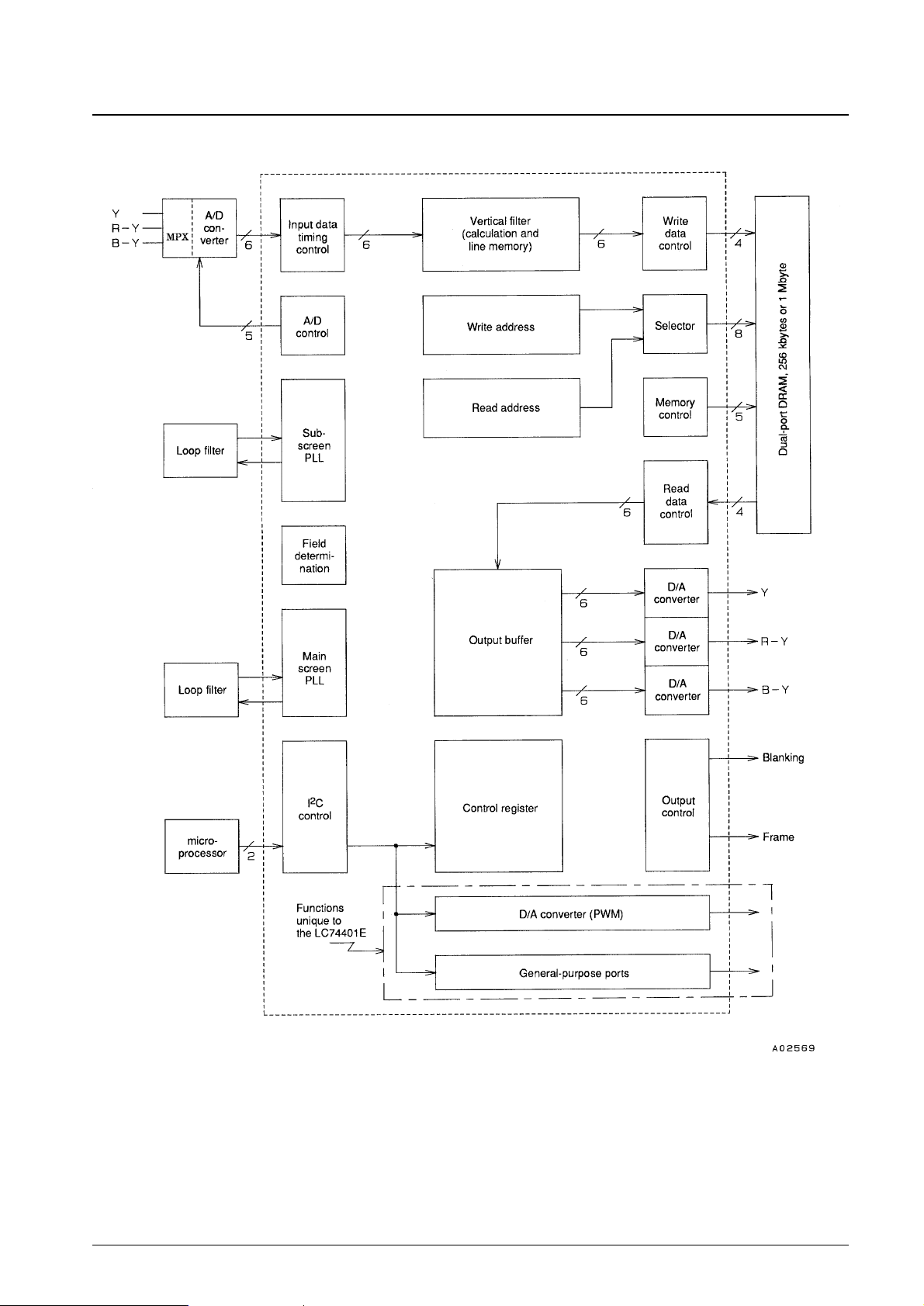
Block Diagram
No. 4872-4/19
LC74401E, 74402, 74402E
Page 5
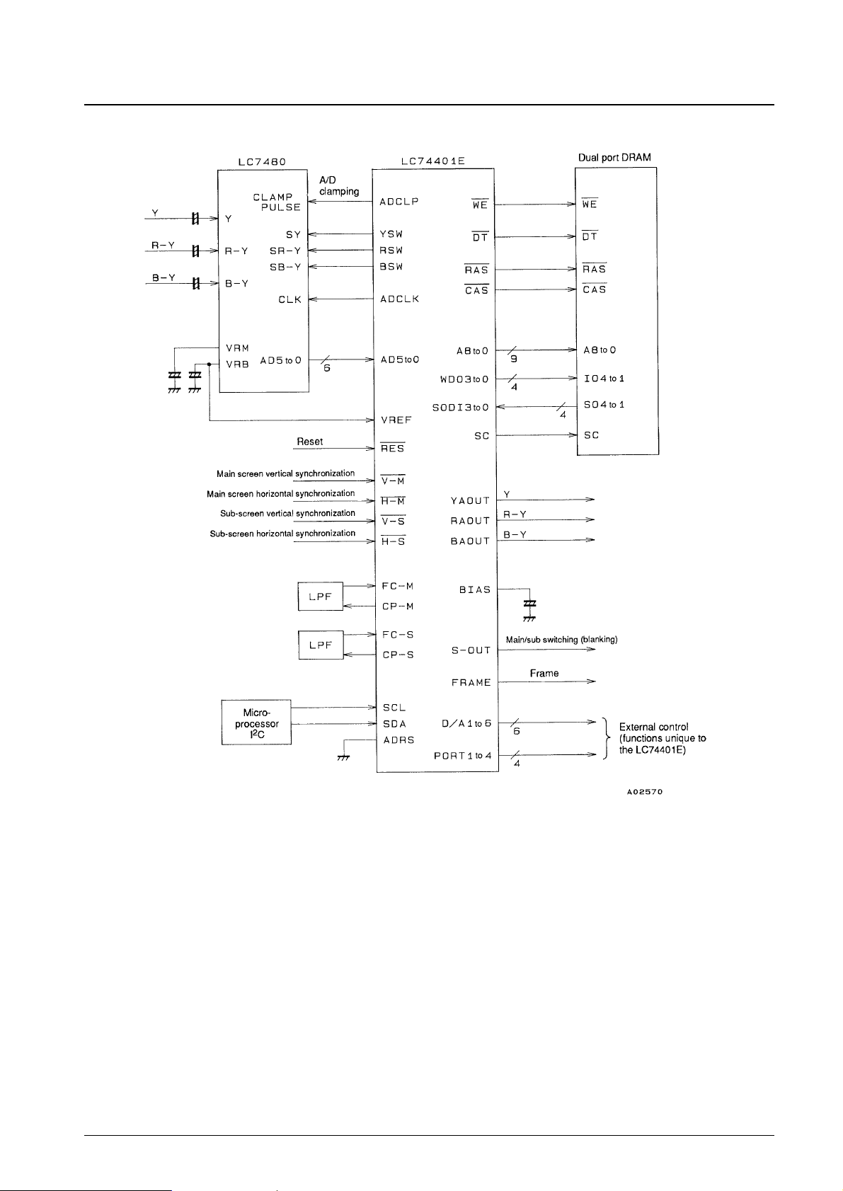
Component-Type PIP System Structure Based on the LC74401E/2/2E and the LC7480
No. 4872-5/19
LC74401E, 74402, 74402E
Page 6

Functional Overview
1. Reduction options
Vertical: Selectable 1/2, 1/3 and 1/4 reduction vertical filter coefficients.
Horizontal: (1/1) to 2/3 to (1/2) to 1/3 to (1/4) to 1/6. Intermediate values are implemented using the aspect
correction function.
2. Number of sub-screens
With 1 Mb of memory: 1 to 4 or (8). * Values in parentheses are for SPLIT mode, where the image quality is
reduced.
With 256 kb of memory: 1 or (2).
3. Static images
With 1 Mb of memory: Frame static image (supported with 2 or fewer screens) or field static images
With 256 kb of memory: Field static image
4. Display position
Screen A: Fixed positions in the four corners
Screen B: Free positioning (Specified by 8 bits in each of the vertical and horizontal directions.)
5. Frame
• On/off selectable
• Two types that differ by insertion method
— Pin frame: The frame position is specified by a high level pin output. (application frame insertion)
— D/A frame: A 50% white or arbitrary color overlapped on the Y, R-Y, and B-Y video signals.
6. Wipe
Twelve types
7. Blanking size
The vertical and horizontal directions can be specified independently (6 bits each)
Sixteen forms can be specified.
8. Blue background
The sub-screen can be set to all blue or all black.
9. Memory clear
Sets the data written to video memory to a fixed value corresponding to a 25% white color.
10. Wide-screen TV support
• Aspect correction function
• Subtitle shifting
The subtitle area can be trimmed and displayed as a sub-screen.
The vertical reduction ratio can be set independently to 1/4, 1/3, or 1/2. The horizontal reduction can be set to
values up to 1/1 using mode 2E.
11. Support for NTSC, PAL, and multi-mode (NTSC-PAL) products
12. External control functions using an I2C interface (LC74401E only)
• Six 8-bit D/A converter circuits built-in (PWM)
• Four general-purpose ports built-in
13. Setting adjustments
Fine adjustment of various settings, including sub-screen position displacement and color shift is supported.
No. 4872-6/19
LC74401E, 74402, 74402E
Page 7

Sub-screen Size
The vertical and horizontal directions are controlled independently.
1. Vertical size
• 1/3 to (3) scan lines are compressed to a single scan line
• 1/4 to (4) scan lines are compressed to a single scan line
2. Horizontal size
• 1/3 to A/D clock: D/A clock = 1:3
• 1/6 to A/D clock: D/A clock = 1:6
The data required for 1/6 reduction is one half that for 1/3 reduction.
• Aspect correction function
The horizontal direction size is adjusted by changing the VCO oscillator frequency (system clock).
This can be adjusted from –30% to +30%.
However, care is required when using this function. See the Application Manual for details.
• 2E mode
If 2E mode is used when 1/3 size is selected, the horizontal direction is expanded by a factor of two.
This is normally used only for special functions such as split mode.
Number of Sub-screens
Between one and eight sub-screens can be specified (when 1 Mb of VRAM is used).
Split mode
Refer to the Application Manual for details on using these modes.
No. 4872-7/19
LC74401E, 74402, 74402E
Page 8

Wipe Function
Wipe operation can be set in the top, bottom, left, and right directions, and in the diagonal direction independently.
After a wipe mode has been set up, it operates automatically each time a sub-screen is switched on or off.
Display Area Function
This function controls the blanking area.
The vertical direction and horizontal direction can be set up independently.
The operating mode is set by setting the wipe function TOP, BOT, LEFT, or RIGHT mode.
Application Example
1. Excluding the masked portion of the letter box screen
2. Subtitle display
3. Small display
No. 4872-8/19
LC74401E, 74402, 74402E
Page 9

Multi-mode
1. When 1 Mb of VRAM is used
• Frame memory processing (FRM = high)
Dynamic images: Frame display (MUL = high, overrun phenomenon occurs)
Static images: Frame display
• Field memory processing (FRM = low, FILD = high)
Dynamic images: Field display (overrun phenomenon occurs)
Static images: Field display
NTSC/PAL (= main/sub)
PAL/NTSC
The sub-screen size ratio (V) will be:
a : b : c : d: = 1 : 0.8 : 0.77 : 0.58
If b and c are used, the size change can be held to 5%.
2. When 256 kb of VRAM are used
Field memory processing (FRM = low, FILD = high)
Dynamic images: Field display (overrun phenomenon occurs)
Static images: Field display
Only one screen can be displayed.
No. 4872-9/19
LC74401E, 74402, 74402E
Page 10

Control Register Table
Note: 1. “0” indicates that the register value is set to 0.
2. When designing an application, be sure to read the Application Manual and check any relevant notes.
3. Addresses 0E to 14 are only valid for the LC74401E.
No. 4872-10/19
LC74401E, 74402, 74402E
Address MSB LSB
(HEX) 7 6 5 4 3 2 1 0
01 SBY STL NT/PAL MUL FILD FRM P-NUM1 P-NUM0 Operating mode 1
02 WRT2 WRT1 WRT0 D-FIX POUT-B POUT-A FVP FHP Operating mode 2
03 VP7 VP6 VP5 VP4 VP3 VP2 VP1 VP0 Screen B display position (V)
04 HP7 HP6 HP5 HP4 HP3 HP2 HP1 HP0 Screen B display position (H)
05 FRM-B FRM-A FRC-B FRC-A YFC5 YFC4 YFC3 YFC2 Frame setting, frame color (Y)
06 RFC5 RFC4 RFC3 RFC2 BFC5 BFC4 BFC3 BFC2 Frame color (R-Y, B-Y)
07 VDF-CO HDF. 2E CL-AJ1 CL-AJ0 FM-AJ1 FM-AJ0 YC-AJ1 YC-AJ0 Filter setting, adjustment 1
08 SIZE-V SIZE-H SPLIT PLL7 PLL6 PLL5 PLL4 PLL3 Sub-screen size, PLL
09 WPE-B WPE-A TOP BOT LEFT RIGHT DIA WP-MOD Wipe setting
0A PHP-M PHP-S VBS5 VBS4 VBS3 VBS2 VBS1 VBS0 Display area (V)
0B DT-AJ1 DT-AJ0 HBS5 HBS4 HBS3 HBS2 HBS1 HBS0 Display area (H)
0C TEXT UPPER M-BLUE M-LVL YL5 YL4 YL3 YL2 Subtitle display setting
0D WV-AJ1 WV-AJ0 WH-AJ1 WH-AJ0 VP-AJ1 VP-AJ0 HP-AJ1 HP-AJ0 Display adjustment 2
0E DAC1-7 DAC1-6 DAC1-5 DAC1-4 DAC1-3 DAC1-2 DAC1-1 DAC1-0 8-bit D/A converter 1 data
0F DAC2-7 DAC2-6 DAC2-5 DAC2-4 DAC2-3 DAC2-2 DAC2-1 DAC2-0 8-bit D/A converter 2 data
10 DAC3-7 DAC3-6 DAC3-5 DAC3-4 DAC3-3 DAC3-2 DAC3-1 DAC3-0 8-bit D/A converter 3 data
11 DAC4-7 DAC4-6 DAC4-5 DAC4-4 DAC4-3 DAC4-2 DAC4-1 DAC4-0 8-bit D/A converter 4 data
12 DAC5-7 DAC5-6 DAC5-5 DAC5-4 DAC5-3 DAC5-2 DAC5-1 DAC5-0 8-bit D/A converter 5 data
13 DAC6-7 DAC6-6 DAC6-5 DAC6-4 DAC6-3 DAC6-2 DAC6-1 DAC6-0 8-bit D/A converter 6 data
14 0 0 0 0 PORT-4 PORT-3 PORT-2 PORT-1 General-purpose port
15 V-1/2 0 0 0 0 0 0 0 Test data
Page 11

Register Data Overview
Note: The register functions at register addresses 0E to 14 can only be used with the LC74401E.
No. 4872-11/19
LC74401E, 74402, 74402E
Address Symbol Description
SBY Standby mode (PLL circuit operating)
STL Static image (All writing stopped)
NT/PAL Format selection (high: NTSC, low: PAL)
01 MUL Multi-mode
FILD Field display selection
FRM Frame memory processing selection
P-NUM1, 0 Number of screen B screens displayed (one to four screens)
WRT2 to 0 Dynamic image setting (write screen specification)
02
D-FIX Memory clear (fixes the memory write data)
POUT-B, A Sub-screen display on/off
FVP, FHP Four corner fixed position (screen A) specification
03 VP7 to 0 Screen B vertical position data
04 HP7 to 0 Screen B horizontal position data
FRM-B, A D/A converter frame on/off
05 FRC-B, A D/A converter frame color register value specification
YFC5 to 2 D/A converter frame color (Y)
06
RFC5 to 2 D/A converter frame color (R-Y)
BFC5 to 2 D/A converter frame color (B-Y)
VDF-CO Vertical filter coefficient specification
HDF, 2E
HDF (horizontal filter on/off when SIZE-H = 1)
07
2E mode (horizontal 2x expansion) on/off when SIZE-H = 0
CL-AJ1, 0 A/D converter clamping position adjustment
FM-AJ1, 0 D/A converter frame left/right thickness adjustment
YC-AJ1, 0 Position adjustment for C (R-Y, B-Y) with respect to Y
SIZE-V Vertical reduction specification H: 1/4 L: 1/3
08
SIZE-H Horizontal reduction specification H: 1/6 L: 1/3
SPLIT Split mode (Doubles the number of screens by splitting the sub-screens horizontally.)
PLL7 to 3 PLL divisor value (10011 is the standard value)
WPE-B, A Wipe or display area function enable
09 TOP to DIA Wipe or display area function shape specification
WP-MOD Wipe or display area function selection (high: wipe)
0A
PHP-M, S Inversion or non-inversion of the field determination result
VBS5 to 0 Display area value setting (vertical direction)
0B
DT-AJ1, 0 Memory control signal (DT) adjustment
HBS5 to 0 Display area value setting (horizontal direction)
TEXT Partial display of an image reduced 1/2 in the vertical direction
UPPER Section specification for partial display in TEXT mode
0C M-BLUE Blue specification in masking mode
M-LVL Y level specification for the masked section
YL-5 to 2 Masking level (data compared to the Y level)
WV-AJ1, 0 Write vertical direction adjustment
0D
WH-AJ1, 0 Write horizontal direction adjustment
VP-AJ1, 0 Display position vertical direction adjustment
HP-AJ1, 0 Display position horizontal direction adjustment
0E DAC1-7 to 0
0F DAC2-7 to 0
10 DAC3-7 to 0
External control D/A converter (8-bit PWM) data
11 DAC4-7 to 0
12 DAC5-7 to 0
13 DAC6-7 to 0
14 PORT-4 to 1 General-purpose port data
15 V-1/2 Vertical reduction specification 1/2
Page 12

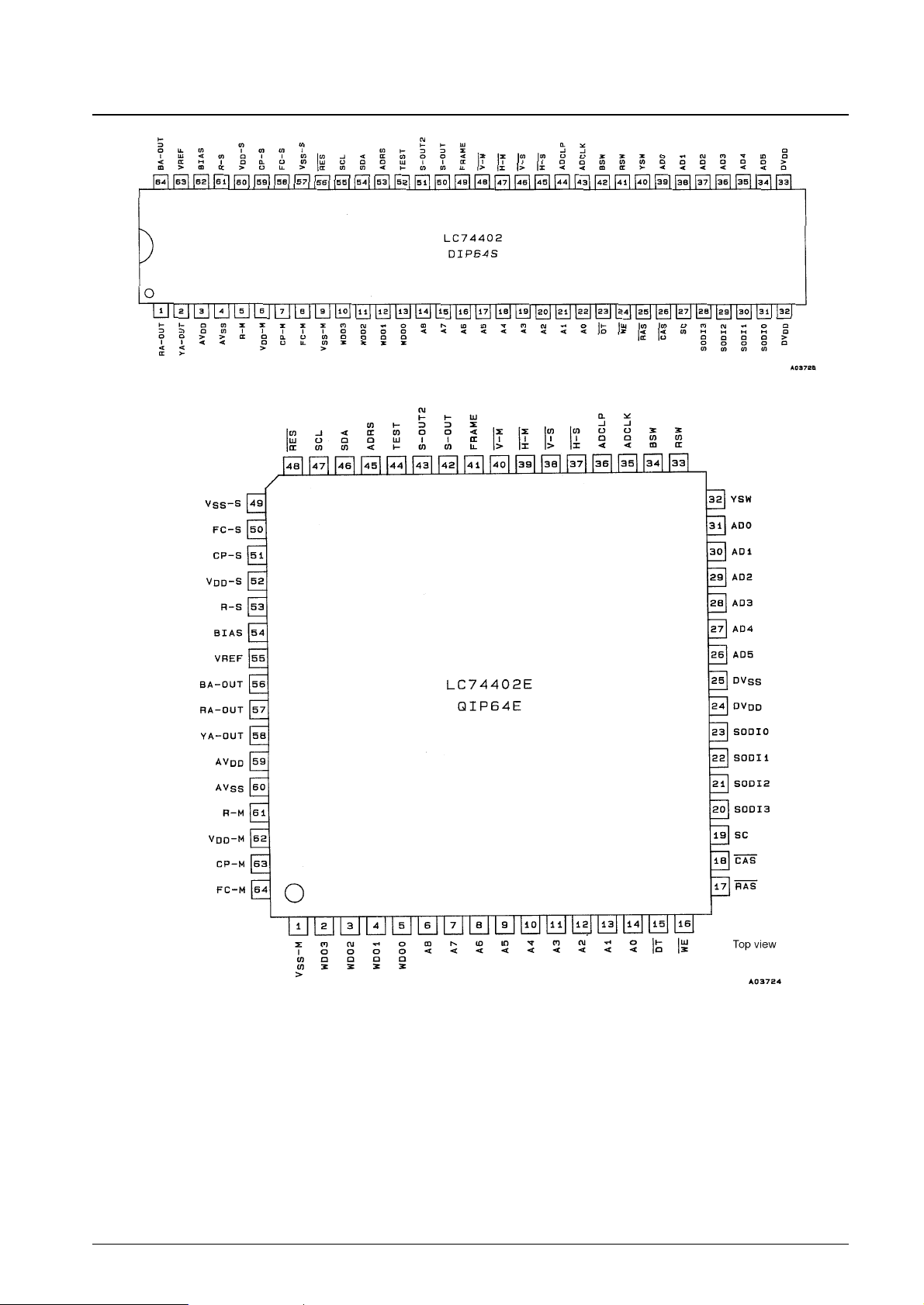
Pin Functions
Pin No. 80E: LC74401E, 64S: LC74402, 64E: LC74402E
No. 4872-12/19
LC74401E, 74402, 74402E
Pin No.
Symbol I/O Connection Functions Circuit type
64S 64E 80E
48 40 53 V-M I
Main screen vertical synchronization signal
(negative polarity)
47 39 50 H-M I
Main screen horizontal synchronization signal
(negative polarity)
46 38 49 V-S I
Sub-screen vertical synchronization signal
(negative polarity)
45 37 48 H-S I
Sub-screen horizontal synchronization signal
(negative polarity)
55 47 61 SCL I
Microprocessor
Serial clock
I
2
C
54 46 60 SDA I/O Serial data
53 45 59 ADRS I V
SS
56 48 62 RES I Initialization circuit Reset
52 44 57 TEST I V
SS
Test (Tied to VSSin normal operation.)
— — 3 PORT1 O
— — 8 PORT2 O
General-purpose ports
— — 15 PORT3 O
— — 20 PORT4 O
10 2 4 WDO3 O
11 3 5 WDO2 O
Memory write data outputs
12 4 6 WDO1 O
Memory
13 5 7 WDO0 O
14 6 9 A8 O MSB
15 7 11 A7 O
16 8 12 A6 O
17 9 13 A5 O
18 10 14 A4 O Memory
19 11 16 A3 O
20 12 17 A2 O
21 13 18 A1 O
22 14 19 A0 O LSB
23 15 21 DT O
24 16 22 WE O
25 17 25 RAS O Memory Control signals
26 18 26 CAS O
27 19 27 SC O
28 20 28 SODI3 I
29 21 29 SODI2 I
Memory read data inputs
30 22 30 SODI1 I
Memory
31 23 31 SODI0 I
— — 63 D/A1 O
— — 58 D/A2 O
— — 52 D/A3 O
PWM D/A converter output
— — 51 D/A4 O
— — 47 D/A5 O
— — 46 D/A6 O
LA7403 or a sync
separator IC
Address
(A8 is left open when
a 256 kbyte external
memory is used.)
Continued on next page.
Page 13

Continued from preceding page.
Pin No. 80E: LC74401E, 64S: LC74402, 64E: LC74402E
Specifications
Absolute Maximum Ratings at Ta = 25 ± 8°C, VSS= 0 V
No. 4872-13/19
LC74401E, 74402, 74402E
Pin No.
Symbol I/O Connection Functions Circuit type
64S 64E 80E
34 26 34 AD5 I MSB
35 27 35 AD4 I
36 28 36 AD3 I
LC7480 Inputs for A/D converted digital data
37 29 37 AD2 I
38 30 38 AD1 I
39 31 39 AD0 I LSB
40 32 40 YSW O Y signal selection
41 33 42 RSW O LC7480 R-Y signal selection MPX switching signals
42 34 43 BSW O B-Y signal selection
43 35 44 ADCLK O LC7480 Sampling clock
44 36 45 ADCLP O LC7480 Clamping pulse
49 41 54 FRAME O LA7403 Frame pulse output
50 42 55 S-OUT O LA7403 Main/sub switching signal
51 43 56 S-OUT2 O — Control signal
32 24 32 DV
DD
Digital power supply
33 25 33 DV
SS
(for logic circuits and line memory)
2 58 74 YA-OUT O Y signal
1 57 73 RA-OUT O LA7403 R-Y signal D/A converter outputs
64 56 72 BA-OUT O B-Y signal
63 55 71 VREF I LC7480
D/A converter analog system settings
62 54 70 BIAS — Capacitor
3 59 75 AV
DD
D/A converter analog system power supply
4 60 76 AV
SS
7 63 79 CP-M O LPF Charge pump output
8 64 80 FC-M I LPF
Oscillator control
voltage input
5 61 77 R-M — Resistor Oscillator range resistor
6 62 78 V
DD
-M
Power supply
9 1 2 V
SS
-M
59 51 67 CP-S O LPF Charge pump output
58 50 66 FC-S I LPF
Oscillator control
voltage input
61 53 69 R-S — Resistor Oscillator range resistor
60 52 68 V
DD
-S
Power supply
57 49 65 V
SS
-S
Main screen
synchronization
VCO
Main screen
synchronization
VCO
Parameter Symbol Conditions Ratings Unit
Maximum supply voltage V
DD
max –0.3 to +7.0 V
Input voltage V
IN
–0.3 to VDD+ 0.3 V
Output voltage V
OUT
–0.3 to VDD+ 0.3 V
Allowable power dissipation Pd max 350 mW
Operating temperature Topr –10 to +70 °C
Storage temperature Tstg –55 to +125 °C
Page 14

Allowable Operating Ranges at Ta = –10 to +70°C, VSS= 0 V
Electrical Characteristics at Ta = 25 ± 2°C, VDD= 5 V ± 10%, VSS= 0 V
Note: 1. Test conditions as follows:
RES: V
DD
, V-M, V-S: 60 Hz, H-M, H-S: 15 kHz
A/D converter data: 1010..., No output load
2. There are four power supply pin systems.
The supply voltages must all be equal, i.e., DV
DD
= AVDD= VDD-M = VDD-S. Descriptions are in terms of VDD.
The grounds must all be equal, i.e., DV
SS
= AVSS= VSS-M = VSS-S. Descriptions are in terms of VSS.
Switching Characteristics at Ta = 25 ± 2°C, VDD= 5 V ± 10%, VSS= 0 V
No. 4872-14/19
LC74401E, 74402, 74402E
Parameter Symbol Conditions
Ratings
Unit
min typ max
Supply voltage V
DD
4.5 5.0 5.5 V
Input high level voltage
V
IH
1 CMOS level 0.7 V
DD
V
V
IH
2 TTL level 2.2 V
Input low level voltage
V
IL
1 CMOS level 0.3 V
DD
V
V
IL
2 TTL level 0.8 V
Reference voltage V
REF
3.4 0.8 V
DD
V
DD
V
Parameter Symbol Conditions
Ratings
Unit
min typ max
Output high level voltage
V
OH
1 Pins CP-M and CP-S: IOH= –1 mA VDD– 1 V
V
OH
2 Pins other than CP-M and CP-S: IOH= –1 mA VDD– 1 V
V
OL
1 Pins CP-M and CP-S: IOL= 1 mA 1.0 V
Output low level voltage V
OL
2 Pins other than CP-M and CP-S: IOL= 2 mA 0.4 V
V
OL
3 With the SDA pin output active: IOL= 3 mA 0.4 V
I
DD
D The DVSSpin 25 mA
Operating current drain
*1
IDDA The AVSSpin 21 mA
I
DD
M The VSS-M pin 2 mA
I
DD
S The VSS-S pin 2 mA
Quiescent current I
DD
S
RES: V
SS
10 µA
with DC signals on the input pins and no output load.
Input leakage current I
LK
VI= VDD, V
SS
–1 +1 µA
Output leakage current I
OZ
Pins CP-M and CP-S; VI= VDD, V
SS
–1 +1 µA
D/A converter output resistance R
DA
150 Ω
Parameter Symbol Conditions
Ratings
Unit
min typ max
Vertical synchronization signal
Pulse width t
VW
1 µs
Rise time t
VR
50 ns
Fall time t
VF
50 ns
Horizontal synchronization signal
Pulse width t
HW
1 µs
Rise time t
HR
50 ns
Fall time t
HF
50 ns
I
2
C timing
SCL frequency t
SCL
100 kHz
Bus release time t
BUF
4.7 µs
Start hold time t
HD
; STA 4.0 µs
SCL low period t
LOW
4.7 µs
SCL high period t
HIGH
4.0 µs
Data hold time t
HD
; DAT 0 µs
Data setup time t
SU
; DAT 250 ns
Rise time t
R
1000 ns
Fall time t
F
300 ns
Stop setup time t
SU
; STO 4.0 µs
Page 15

Synchronization Signal
Sub-Screen Digital Processing Specifications
Note: 1. When the PLL divisor has the standard value, i.e., PLL7 to PLL3 = 10011.
2. Approximate values.
(The number of horizontal dots depends on the frame width adjustment, and the vertical H count depends on address correction.)
No. 4872-15/19
LC74401E, 74402, 74402E
Item NTSC (fH= 15734 Hz) PAL (fH= 15625 Hz)
Sequence Y, R-Y, Y, B-Y, Y, –, Y, –, ...
Frequency 640 f
H
fT(MHz) 10.070 10.000
Y only 320 f
H
Sampling f
TY
5.035 5.000
R-Y only 80 f
H
f
TR
1.258 1.250
B-Y only 80 f
H
f
TB
1.258 1.250
Quantization bits 6 bits
Y signal 960 f
H
f
CY
15.105 15.000
D/A converter clock (MHz)
*1
R-Y signal 240 f
H
f
CR
3.776 3.750
B-Y signal 240 f
H
f
CB
3.776 3.750
Horizontal dots 384
Y only 256
Write R-Y only 64
B-Y only 64
Vertical H count 80 84
Horizontal dots 370
Y only 250
Read and display
*2
R-Y only 60
B-Y only 60
Vertical H count 77 83
Page 16

Initialization
1. RES pin: Reset
The RES pin must be set low when power is first applied.
2. Internal control registers
These LSIs go to the standby state (SBY = high) after a reset. When developing microprocessor software, be sure to
send data to all registers. Also be sure to send zero data to the zero registers at addresses 14H and 15H.
I2C Control
Data format
Data 1 is stored at register address A1. For data 2, A1 is incremented and data 2 is stored at A1 + 1.
Slave Address
Synchronization Signal Input
1. Sync separator
The LC74401E requires sync separated (including AFC processing) V and H signals for both the main and subscreens. Since V is used for frame determination and H is used as the PLL reference signal, these signals must be
input reliably.
• The standard values are set up assuming that the H-M and H-S inputs are delayed about 1 µs from the video signal
horizontal synchronization signal.
• Equalizing pulses must be removed.
• Since noise in the synchronization signal will disrupt the screen image, care must be used in the layout of these lines.
• We recommend turning off sub-screen display when the synchronization signals are unstable, since such instability
can disrupt the sub-screen image.
No. 4872-16/19
LC74401E, 74402, 74402E
A6 A5 A4 A3 A2 A1 A0 R/W
0 0 1 0 0 1 1
Page 17

2. Field determination circuit
Since the field is determined by the phase difference between the falling edges of the V and H signals, these signals
must be input with the timing shown in the figure.
Here, a and b must be: a = 0.02 to 0.40 H, b = 0.60 to 0.98 H.
The synchronization signal pulse widths are: t
WV
> 1 µs, tWH> 1 µs.
Clamping Pulses
1. A/D converter clamping
Since clamping pulses are output with the timing shown in the figure, they must set to fall in the pedestal range. On a
reset or during standby mode, the H-S input signal becomes a positive polarity signal, and is output as such.
Note: Here, t3 and t4 must be: t3 > 0 µs, t4 > 0.5 µs.
2. D/A converter clamping
The digital data for the regions A is as follows:
Y D/A converter input: 000000
R-Y D/A converter input: 100000
B-Y D/A converter input: 100000
Clamping is applied on the main screen horizontal synchronization signal.
No. 4872-17/19
LC74401E, 74402, 74402E
Page 18

External Control Output Timing
1. A/D converter (LC7480) related signals
Note: Since these are high speed signals, care must be taken to keep their lines as short as possible.
2. Clamping related signals
Note: The FRAME signal is only output in D/A converter frame off mode.
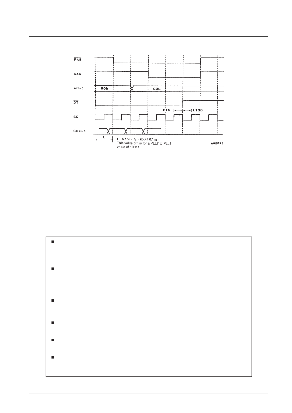
3. Video memory related signals
• Data write signals (page mode)
• Refresh signals (CAS before RAS)
No. 4872-18/19
LC74401E, 74402, 74402E
Page 19
PS No. 4872-19/19
LC74401E, 74402, 74402E
3. Data transfer → serial read
Note: 1. Since these are high speed signals, care must be taken to keep their lines as short as possible.
2. Contact your Sanyo representative when determining the memory to use.
This catalog provides information as of September, 1998. Specifications and information herein are
subject to change without notice.
Specifications of any and all SANYO products described or contained herein stipulate the performance,
characteristics, and functions of the described products in the independent state, and are not guarantees
of the performance, characteristics, and functions of the described products as mounted in the customer’s
products or equipment. To verify symptoms and states that cannot be evaluated in an independent device,
the customer should always evaluate and test devices mounted in the customer’s products or equipment.
SANYO Electric Co., Ltd. strives to supply high-quality high-reliability products. However, any and all
semiconductor products fail with some probability. It is possible that these probabilistic failures could
give rise to accidents or events that could endanger human lives, that could give rise to smoke or fire,
or that could cause damage to other property. When designing equipment, adopt safety measures so
that these kinds of accidents or events cannot occur. Such measures include but are not limited to protective
circuits and error prevention circuits for safe design, redundant design, and structural design.
In the event that any or all SANYO products (including technical data, services) described or contained
herein are controlled under any of applicable local export control laws and regulations, such products must
not be exported without obtaining the export license from the authorities concerned in accordance with the
above law.
No part of this publication may be reproduced or transmitted in any form or by any means, electronic or
mechanical, including photocopying and recording, or any information storage or retrieval system,
or otherwise, without the prior written permission of SANYO Electric Co., Ltd.
Any and all information described or contained herein are subject to change without notice due to
product/technology improvement, etc. When designing equipment, refer to the “Delivery Specification”
for the SANYO product that you intend to use.
Information (including circuit diagrams and circuit parameters) herein is for example only; it is not
guaranteed for volume production. SANYO believes information herein is accurate and reliable, but
no guarantees are made or implied regarding its use or any infringements of intellectual property rights
or other rights of third parties.
 Loading...