

Page 1
Any and all SANYO products described or contained herein do not have specifications that can handle
applications that require extremely high levels of reliability, such as life-support systems, aircraft’s
control systems, or other applications whose failure can be reasonably expected to result in serious
physical and/or material damage. Consult with your SANYO representative nearest you before using
any SANYO products described or contained herein in such applications.
SANYO assumes no responsibility for equipment failures that result from using products at values that
exceed, even momentarily, rated values (such as maximum ratings, operating condition ranges,or other
parameters) listed in products specifications of any and all SANYO products described or contained
herein.
CMOS IC
DTMF Receiver
Ordering number:ENN3003B
LC7385, 7385M
SANYO Electric Co.,Ltd. Semiconductor Company
TOKYO OFFICE Tokyo Bldg., 1-10, 1 Chome, Ueno, Taito-ku, TOKYO, 110-8534 JAPAN
Overview
The LC7385, 7385M CMOS DTMF Receiver ICs inte grate
bandsplit filter and digital decoder functions for the 16
DTMF digits used in touch-tone telephone systems.
Features
• Single +5V power supply.
• Decodes all 16 DTMF digits.
• Built-in differential input amplifier.
• On-chip filters, including
· Dial tone filter.
· High-group filter.
· Low-group filter.
• User-selectable acquisition and release times.
• Pin-selectable 4-bit hexadecimal or binary-coded 2-of-8
output.
• 3-state data outputs facilitate microcontroller or other
peripheral interfaces.
• Standby mode.
• Low-power double-poly CMOS process.
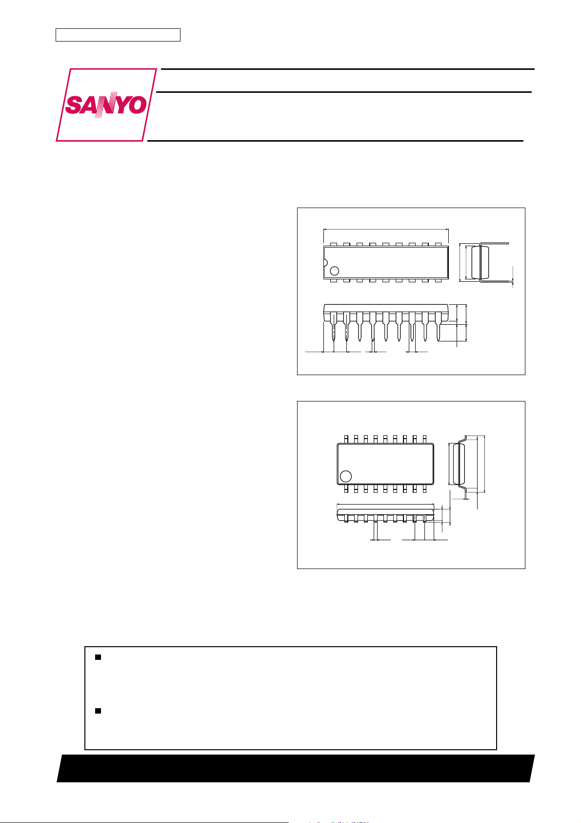
• LC7385 : 18-pin DIP package.
LC7385M : 18-pin MFP package.
Package Dimensions
unit:mm
3007B-DIP18
[LC7385]
24.0
18
1
(1.84)
2.54
unit:mm
3095-MFP18
[LC7385M]
18
10
6.4
7.62
0.25
9
(3.25)
3.85max
3.3
1.20.5
10
0.51min
SANYO : DIP18
1
12.6
0.35
51001TN (KT)/2090YT/D238TA, TS No.3003–1/8
9
1.27
5.4
0.15
1.8max
1.5
0.1
1.22
SANYO : MFP18
6.35
0.625
7.6
Page 2
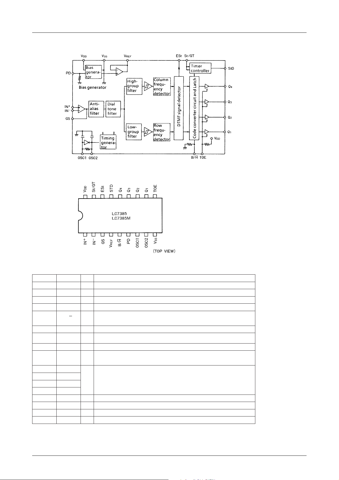
Block Diagram
Pin Assignment
LC7385, 7385M
Pin Functions
.oNniPemaNO/InoitpircseD
1NI
2NI
3SGO .tuptuoreifilpmatupnI
4V
5H/BI
6DPI HGIHottesnehwedomybdnatS
7
8
9V
01EOTI
111Q
212Q
313Q
414Q
51DtSO .emitdraugtessdeecxenoitarudriapenotdilavnehwHGIHseoG
61tSEO .detcetedsieriapenotdilavnehwHGIHseoG
71TG/tSO/I.emitdraugtesotdesU
81V
+
–
FER
1CSO
2CSO
SS
DD
15 14
18 17
16
12345
I.tupnignitrevni-nonreifilpmatupnI
ItupnignitrevnireifilpmatupnI
OV(tuptuoegatlovecnerefeR
I
O
Otuptuoatadetats-3
13 12 11
678
DD
HGIHnehw8-fo-2yraniB
WOLnehwlamicedaxeH
.V0yllamroN.ylppusrewoP
HGIHnehwdelbanE
.V5yllamroN.ylppusrewoP
10
9
)2/
:noitcelestamroftuptuo4Qot1Q
.2CSOdna1CSOneewtebdetcennocsilatsyrczHM545975.3.snipkcolC
:noitcelestuptuoetats-34Qot1Q
WOLnehwecnadepmi-hgiH
No.3003–2/8
Page 3
LC7385, 7385M
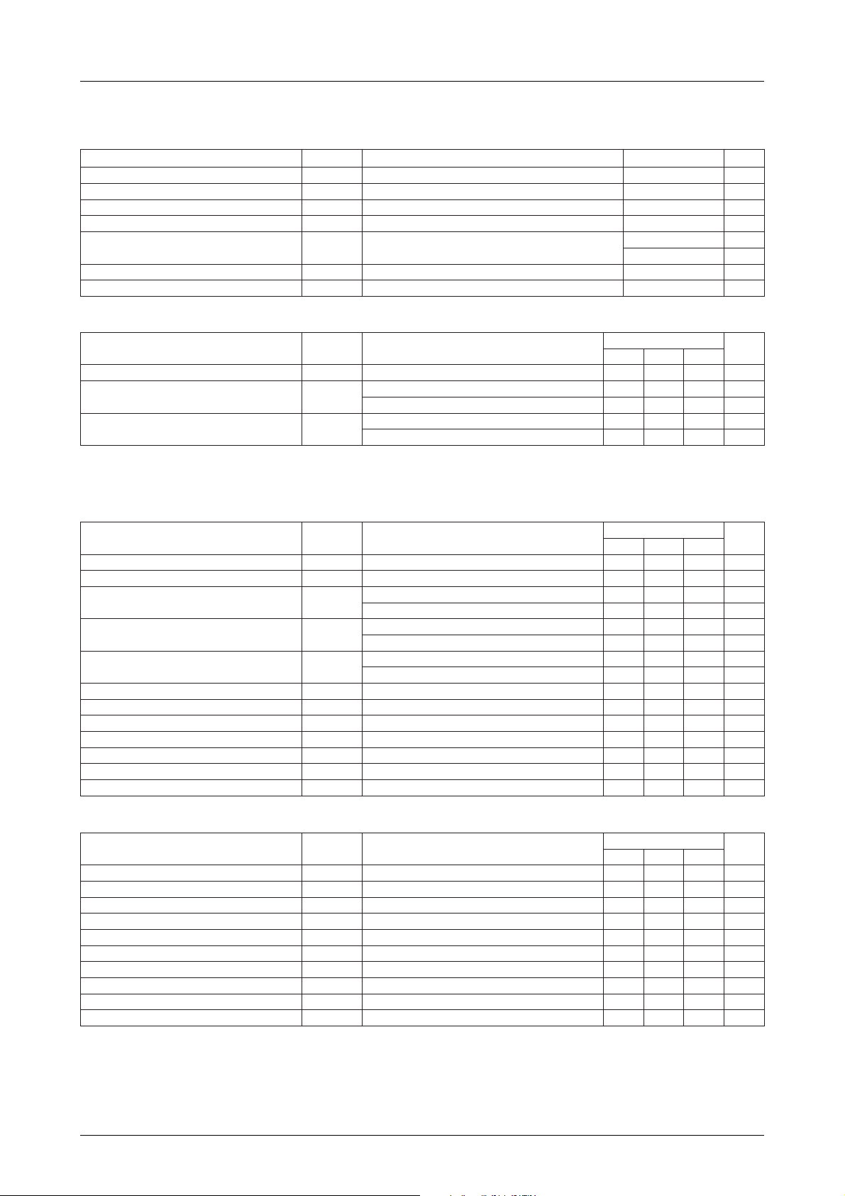
Specifications
Absolute Maximum Ratings at Ta=25±2˚C, VSS=0V
retemaraPlobmySsnoitidnoCsgnitaRtinU
egatlovylppusmumixaMV
egatlovtupnIV
tnerructupnII
egatlovtuptuOV
noitapissidrewopelbawollAxamdP
erutarepmetgnitarepOrpoT 58+ot04–
erutarepmetegarotSgtsT 521+ot05–
Allowable Operating Conditions at Ta=–40 to +85˚C, VSS=0V
retemaraPlobmySsnoitidnoC
egatlovgnitarepOV
egatlovlevel-hgihtupnIV
egatlovlevel-woltupnIV
Note : When soldering the 18-pin MFP package, solder it manually or use the infrared reflow method.
Do not use the dip-soldering method. The conditions for the infrared reflow method are 235°C max., 10s.
xam 0.7+ot3.0–V
DD
NI
NI
TUO
–40˚C≤Ta≤+85°C
nimpytxam
DD
HI
LI
01,6sniP
5niP
01,6sniP
5niP
57.452.5V
V7.0
DD
V58.0
DD
Vot3.0–
DD
Vot3.0–
DD
sgnitaR
3.0+V
01+ot01–Am
3.0+V
052:81-PIDWm
081:81-PFMWm
˚C
˚C
V
V
V3.0
V
DD
V51.0
V
DD
tinU
DC Electrical Characteristics at T a=25±2˚C, VDD=5V, VSS=0V
retemaraPlobmySsnoitidnoC
tnerrucylppusgnitarepOI
tnerrucylppusybdnatSI
tnerruclevel-hgihtuptuOI
tnerruclevel-woltuptuOI
tnerructuptuoetats-FFO
tnerruclevel-hgihtupnII
tnerruclevel-woltupnII
tnerruc)ecruos(pu-lluPI
tnerruc)knis(nwod-lluPI
egatlovdlohserhtTG/tSV
V
FER
V
FER
egatlovtuptuoV
ecnatsisertuptuoR
)po( 0.30.7Am
DD
)ts(DD
HO
LO
I
HZO
I
LZO
HI
LI
OS
IS
TST
FER
FER
V5=DP 001Aµ
V
TUO
V
TUO
V
TUO
V
TUO
V
NI
V
NI
71niP53.2V
4niP1kΩ
71nip,V6.4=0.3–2.1–Am
71nip,V4.0=2.10.3Am
V,V0=EOT
TUO
V,V0=EOT
TUO
01,2,1snip,V5= 01Aµ
6,5,2,1snip,V0=01–Aµ
01nip,V0=EOT51–5–Aµ
6,5snip,V5=H/B,DP551Aµ
4nip,daoloN4.27.2V
Input Amplifier Characteristics at Ta=25±2˚C, VDD=5V, VSS=0V
retemaraPlobmySsnoitidnoC
egatlovtesffotupnIV
tnerructesffotupnII
noitcejerylppusrewoPRRSPzHk106Bd
noitcejeredomnommoCRRMC 06Bd
niagegatlovpool-nepOA
htdiwdnaBniaGBd0f
egatlovtuptuomumixaMV
daoleviticapacelbareloTC
daolevitsiserelbareloTR
egnaredomnommoCV
OI
VSS≤VNI≤V
OI
O
T
RL≥ k001 Ω 5.4p-pV
O
L
L
MC
DD
daoloN0.3p-pV
sgnitaR
nimpytxam
61,51,41,31,21,11snip,V6.4=8.0–4.0–Am
61,51,41,31,21,11snip,V4.0=0.15.2Am
41,31,21,11snip,V5=01Aµ
41,31,21,11snip,V5=01–Aµ
sgnitaR
nimpytxam
52–52+Vm
001±An
56Bd
5.1zHM
001Fp
05kΩ
tinU
tinU
No.3003–3/8
Page 4

LC7385, 7385M
AC Characteristics at Ta=25±2˚C, VDD=5V, VSS=0V, f
retemaraPlobmySsnoitidnoC
levellangistupnidilaV 9,6,5,3,2,192–1.1mBd
timiltpeccatsiwT 11,9,6,3,201±Bd
timiltpeccanoitaivedycneuqerF9,5,3,2
timiltpeccanoitaivedycneuqerF5,3,25.3±%
ecnarelotenotdrihT 01,9,5,4,3,261–Bd
ecnarelotenotlaiD 01,9,8,5,4,3,281+Bd
ecnarelotesioN 01,9,7,5,4,3,221–Bd
emitnoitcetedtneserpenoTt
emitnoitcetedtnesbaenoTt
tpeccanoitarudenoTt
tcegernoitarudenoTt
tpeccaesuaptigidretnIt
tcejeresuaptigidretnIt
tS(yalednoitagaporP → )QtQPdaoloN,V5=EOT811sµ
tS(yalednoitagaporP → )DtSt
Q(pu-tesatadtuptuO → )DtSt
yaledelbanetuptuOt
yaledelbasidtuptuOt
ycneuqerfkcolCf
daoleviticapackcolCC
PD
AD
CER
JER
DI
OD
DTSP
DTSQ
R
ETP
L
R
DTP
L
CSO
OX
2CSO 03Fp
=3.579545MHz
OSC
nimpytxam
.margaidgnimiteeS
.tnemtsujdaemitdraugeeS.elbatsujdA
daoloN,V5=EOT21sµ
daoloN,V5=EOT5.4sµ
C,k01=
Fp05=05001sn
L
C,k01=
Fp05=003sn
L
51141sm
5.00.45.8sm
04sm
04sm
9575.35975.31385.3zHM
sgnitaR
tinU
%5.1±
zH2±
02sm
02sm
Conditions
1. dBm=decibels avove or below a reference power of 1mW into a 600Ω load.
2. All 16 DTMF tones.
3. 40ms DTMF tone duration and 40ms pause duration.
4. Nominal DTMF frequencies.
5. Both tones in composite signal have an equal amplitude.
6. Tone pair deviated by ±1.5% ±2Hz.
7. Bandwidth limited (0 to 3kHz) Gaussian noise.
8. 350Hz and 440Hz +2% dial tone frequencies.
9. Error rate better than 1 in 10,000.
10. Referenced to lowest level frequency component in DTMF signal.
11. Twist=ratio of high-frequency tone level to low-frequency tone level.
Single-Ended Input Configuration
No.3003–4/8
Page 5

Timing Diagram
LC7385, 7385M
No.3003–5/8
Page 6

Decode Table
LFHFYEKEOT
796
796
796
077
077
077
258
258
258
149
149
149
796
077
258
149
–
9021
6331
7741
9021
6331
7741
9021
6331
7741
6331
9021
7741
3361
3361
3361
3361
–
Note : Z=High impedance
DTMF Dialing Matrix
LC7385, 7385M
"L"=H/B"H"=H/B
4Q3Q2Q1Q4Q3Q2Q1Q
L
L
L
L
H
L
L
1
2
3
4
5
6
7
8
9
0
*
#
A
B
C
D
–
H
H
H
H
H
H
H
H
H
H
H
H
H
H
H
H
L
L
L
L
L
L
H
L
H
L
H
L
H
L
L
H
L
H
L
H
L
H
H
H
H
H
H
H
H
H
L
L
Z
Z
L
H
H
H
L
L
H
L
L
H
H
H
L
L
H
L
L
H
H
H
L
L
H
L
L
H
H
H
L
L
Z
Z
L
L
L
L
L
H
H
H
H
H
H
L
L
H
H
Z
L
L
H
H
H
L
L
L
H
H
H
L
H
L
H
Z
mWORnLOC
H
L
L
H
L
L
H
L
L
H
L
L
H
L
L
H
H
L
L
L
L
H
H
H
H
H
H
H
H
H
Z
Z
No.3003–6/8
Page 7

LC7385, 7385M
Guard Time Setting Guard Time Adjustment
Component values are chosen using the following formula :
t
REC=tDP+tGTP
tID=tDA+t
(a) Basic Circuit
t
GTP
t
GTA
(b) t
GTP<tGTRA
t
GTP=R1 R2
t
GTA=R1
GTA
=RC · In [VDD/(VDD–V
=RC · In (VDD/V
TST
)
/(R1+R2) · C · In [VDD/(VDD–V
C · In (VDD/V
TST
)
TST
)]
)]
TST
(c) t
GTP>tGTA
t
GTP=R1
t
GTA=R1 R2
C · In [VDD/(VDD–V
/(R1+R2) · C · In (VDD/V
Differential Input Configuration
Example of component values
C1=C2=0.01µF
R1=R2=R5=100kΩ
R4=60kΩ, R3=37.5kΩ
TST
)]
)
TST
R4R
R4+R
5
5
R3=
Voltage gain : AV=
Input impedance=
R
5
R
1
2
2 √ R
2
1
1
+
2πf
C1
No.3003–7/8
Page 8

LC7385, 7385M
Specifications of any and all SANYO products described or contained herein stipulate the performance,
characteristics, and functions of the described products in the independent state, and are not guarantees
of the performance, characteristics, and functions of the described products as mounted in the customer's
products or equipment. To verify symptoms and states that cannot be evaluated in an independent device,
the customer should always evaluate and test devices mounted in the customer's products or equipment.
SANYO Electric Co., Ltd. strives to supply high-quality high-reliability products. However, any and all
semiconductor products fail with some probability. It is possible that these probabilistic failures could
give rise to accidents or events that could endanger human lives, that could give rise to smoke or fire,
or that could cause damage to other property. When designing equipment, adopt safety measures so
that these kinds of accidents or events cannot occur. Such measures include but are not limited to protective
circuits and error prevention circuits for safe design, redundant design, and structural design.
In the event that any or all SANYO products(including technical data,services) described or
contained herein are controlled under any of applicable local export control laws and regulations,
such products must not be exported without obtaining the export license from the authorities
concerned in accordance with the above law.
No part of this publication may be reproduced or transmitted in any form or by any means, electronic or
mechanical, including photocopying and recording, or any information storage or retrieval system,
or otherwise, without the prior written permission of SANYO Electric Co. , Ltd.
Any and all information described or contained herein are subject to change without notice due to
product/technology improvement, etc. When designing equipment, refer to the "Delivery Specification"
for the SANYO product that you intend to use.
Information (including circuit diagrams and circuit parameters) herein is for example only ; it is not
guaranteed for volume production. SANYO believes information herein is accurate and reliable, but
no guarantees are made or implied regarding its use or any infringements of intellectual property rights
or other rights of third parties.
This catalog provides information as of May, 2001. Specifications and information herein are subject to
change without notice.
PS No.3003–8/8
 Loading...