

Page 1

Ordering number : ENN6124
D2200RM (OT) No. 6124-1/17
Overview
The LC73815M is a telephone IC that integrates on a
single chip both an FSK modem, which receives pre-call
reporting services such as caller ID and performs other
data send/receive functions, and a DTMF receiver circuit
that can handle remote control functions for telephone
answering machine applications.
Applications
Pre-call reporting services, such as Caller ID, reception,
other data send/receive functions, and remote control of
telephone answering machine applications.
Features
• FSK modem (1200 bps)
• Circuit that automatically generates the start and stop
bits used during FSK modulation
• Circuit that automatically generates the continuous mark
signal at the start of transmission in FSK modulation
mode
• Circuit that automatically inserts the idle bits (5 or more
bits) used in FSK modulation mode
• Built-in clock synchronous I/O shift register
• Detection of all 16 DTMF signals
• Digital guard timer circuits for the DTMF signal
detection signal pins
• Operating voltage range: 4.5 to 5.5 V
• Low-power mode that can contribute to energy savings
• 36-pin package (MFP-36S)
Package Dimensions
unit: mm
3129-MFP36S
0.25
15.3
1
18
36
19
0.85
0.4
0.8
2.5max
2.25
0.1
7.9
9.2
10.5
0.65
SANYO: MFP36S
[LC73815M]
LC73815M
SANYO Electric Co.,Ltd. Semiconductor Company
TOKYO OFFICE Tokyo Bldg., 1-10, 1 Chome, Ueno, Taito-ku, TOKYO, 110-8534 JAPAN
FSK 1200 Baud Modem and DTMF Receiver
CMOS IC
Any and all SANYO products described or contained herein do not have specifications that can handle
applications that require extremely high levels of reliability, such as life-support systems, aircraft’s
control systems, or other applications whose failure can be reasonably expected to result in serious
physical and/or material damage. Consult with your SANYO representative nearest you before using
any SANYO products described or contained herein in such applications.
SANYO assumes no responsibility for equipment failures that result from using products at values that
exceed, even momentarily, rated values (such as maximum ratings, operating condition ranges, or other
parameters) listed in products specifications of any and all SANYO products described or contained
herein.
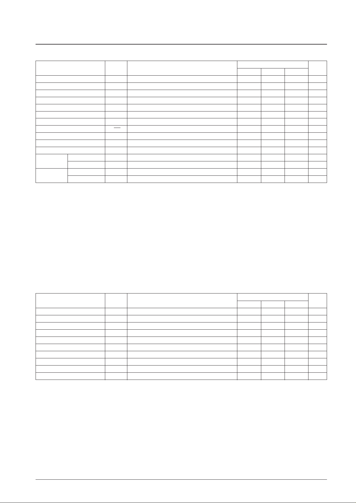
Parameter Symbol Conditions Ratings Unit
Maximum supply voltage V
DD
max –0.3 to +7.0 V
Maximum input voltage V
IN
max –0.3 to VDD+ 0.3 V
Maximum input current I
IN
max –10 to +10 mA
Allowable power dissipation Pd max Ta ≤ 70°C 250 mW
Operating temperature Topr –30 to +70 °C
Storage temperature Tstg –40 to +125 °C
Specifications
Absolute Maximum Ratings at Ta = 25°C, VSS= 0 V
Page 2

No. 6124-2/17
LC73815M
Parameter Symbol Conditions
Ratings
Unit
min typ max
Supply voltage V
DD
4.5 5.0 5.5 V
I
DD
(OP1) VDD= 5.0 V, when the DTMF receiver is used. 5.5 10 mA
Operating current drain I
DD
(OP2) VDD= 5.0 V, during FSK reception 7.5 15 mA
I
DD
(OP3) VDD= 5.0 V, during FSK transmission 7.5 15 mA
Quiescent current I
DD
(ST) RES pin = low 10 µA
Oscillator frequency f
OSC
3.5757965 3.579545 3.583125 MHz
Allowable Operating Ranges at Ta = –30 to +70°C, VSS= 0 V
Parameter Symbol Conditions
Ratings
Unit
min typ max
High-level input voltage
V
IH
Pins other than ACK and RES 0.7 V
DD
V
V
IHS
The ACK and RES input pins 0.8 V
DD
V
Low-level input voltage
V
IL
Pins other than ACK and RES 0.3 V
DD
V
V
ILS
The ACK and RES input pins 0.2 V
DD
V
Input leakage current
V
IH
VIN= V
DD
10 µA
I
IL
VIN= GND –10 µA
High-level output current I
OH
V
OUT
= VDD– 0.4 V –0.8 –0.4 mA
Low-level output current I
OL
V
OUT
= 0.4 V 1.0 2.5 mA
DC Electrical Characteristics at Ta = 25°C, VDD= 5 V, VSS= 0 V
Parameter Symbol Conditions
Ratings
Unit
min typ max
Input signal detection level FSK reception –38 +3 dBm
Reception data transmission speed FSK 1188 1200 1212 baud
Reception frequency
FSK (Mark) 1180 1250 1320 Hz
FSK (Space) 2070 2150 2280 Hz
f
ACK
1 MHz
Shift register data shift speed t
CKL
500 ns
t
CKH
500 ns
External oscillator input EXTOI 0.5 Vrms
B/V = H FSK (Mark) 1200 Hz
FSK transmission frequency
(BELL202) FSK (Space) 2204 Hz
B/V = L FSK (Mark) 1300 Hz
(V.23) FSK (Space) 2101 Hz
FSK output amplitude 0.5 0.8 Vp-p
Transfer rate 1200 bps
FSK modulation delay time t
DDEM
See the timing chart. 0 0.83 ms
Data output setup time t
SDATA
See the timing chart. 0 0.42 0.83 ms
DR output setup time t
SDR
See the timing chart. 2.2 3.3 µs
ACK - DATA setup time t
SCKD
See the timing chart. 0 300 ns
ACK - DR setup time t
SCKDR
See the timing chart. 1.1 9.0 µs
AC Electrical Characteristics 1 (FSK reception/transmission) at Ta = 25°C, VDD= 5 V, VSS= 0 V, f
OSC
= 3.579545 MHz
Conditions: For the dBm ratings, 0 dBm is defined to be a 1 mW output into a 600 Ω load.
Page 3
No. 6124-3/17
LC73815M
Parameter Symbol Conditions
Ratings
Unit
min typ max
Input signal detection level 1, 2, 3, 5, 6, 9 –45 +0 dBm
Allowable twist 2, 3, 6, 9, 11 ±10 dB
Frequency detection band 2, 3, 5, 9
±1.5% ±2 Hz
Frequency non-detection band 2, 3, 5 ±3.5 %
Allowable third tone 2, 3, 4, 5, 9, 10 –16 dB
Allowable dial tone 2, 3, 4, 5, 8, 9, 10 22 dB
Allowable noise 2, 3, 4, 5, 7, 9, 10 –12 dB
Input signal invalid time t
REC
See the timing chart. 20 ms
Input signal valid time t
REC
See the timing chart. 45 ms
Interdigit pause invalid time t
DO
See the timing chart. 20 ms
Interdigit pause valid time t
ID
See the timing chart. 40 ms
Guard time
(Present) t
GDP
See the timing chart. 30 ms
(Absent) t
GDA
See the timing chart. 20 ms
Input signal (Present) t
DP
See the timing chart. 3 20 ms
detection time (Absent) t
DA
See the timing chart. 0.5 20 ms
AC Electrical Characteristics 2 (DTMF reception) at Ta = 25°C, VDD= 5 V, VSS= 0 V, f
OSC
= 3.579545 MHz
Parameter Symbol Conditions
Ratings
Unit
min typ max
Input offset voltage V
IO
–25 +25 mV
Input offset current I
IO
VSS≤ VIN≤ V
DD
±100 nA
Power supply rejection ratio PSRR 1 kHz 60 dB
Common-mode rejection ratio CMRR 60 dB
Open loop voltage gain AO 65 dB
0 dB bandwidth f
T
1.5 MHz
Maximum output voltage V
O
RL≥ 100 kΩ VDD– 0.5 Vp-p
Allowable load capacitance C
L
100 pF
Allowable load resistance R
L
50 kΩ
Common-mode input voltage range V
CM
No load 3.0 Vp-p
Input Amplifier Characteristics at Ta = 25°C, VDD= 5 V, VSS= 0 V, f
OSC
= 3.579545 MHz
Conditions 1. The 0 dBm level is defined to be a 1 mW output into a 600 Ω load.
2. All combinations of the 16 DTMF signals.
3. A 40 ms DTMF signal period, and a 40 ms pause period
4. The nominal frequencies are used for DTMF signals.
5. The signal levels of the low group and high group signals are identical.
6. The tolerance for DTMF signal frequency is within ±1.5% or ±2 Hz.
7. Gaussian noise with a band of 0 to 3 kHz
8. Dial tone pair of 350 and 440 Hz
9. The error ratio is under 1 error in 10,000 operations.
10. Referenced to the frequency component with the lowest level in the DTMF signal.
11. Twist: the ratio of the high group tone level to the low group tone level
Note: This IC contains a Switched Capacitor Filter (SCF) circuit on chip.
Since the internal SCF clock frequency is OSC/56 (= 63.92 kHz), a power supply related noise whose frequency is OSC/56 multiplied by some integer
±3 kHz will prevent the ratings shown above from being achieved.
Therefore, care must be taken for the power supply related noise.
Page 4
No. 6124-4/17
LC73815M
Pin Functions
Pin No. Pin I/O Function
1IN
+
I Differential operational amplifier noninverting input
2IN
–
I Differential operational amplifier inverting input
3 GS O Differential operational amplifier output
4 AGND O IC internal analog ground output
5NC
6 FSKOUT O FSK signal output. This is an npn transistor emitter-follower output.
7 AGCO O Connect to pin 8 through a capacitor. Make no other connections to this pin.
8 FSKIN I Connect to pin 7 through a capacitor. Make no other connections to this pin.
9NC
10 AGND I IC internal analog ground input
11 NC
12 TESTI I IC test input. This pin must be tied low during normal operation.
13 B/V I
Transmission FSK frequency switching input (Bell 202, V.23)
High: Bell 202, Low: V.23
14 NC
15 OSCIN I Connect a 3.579545 MHz oscillator element between these pins. An external 3.579545 MHz may also be supplied.
16 OSCOUT O (Consult oscillator element manufacturers concerning the combination of their products with this IC.)
17 NC
18 V
SS
Ground
19 V
DD
I Power supply. Connect a capacitor of at least 0.1 µF between this pin and GND.
20 NC
21 S/R I FSK send/receive mode switching input. High: Send, Low: Receive.
22 F/D I
FSK modem/DTMF receiver operating mode switching input.
High: FSK modem, Low DTMF receiver.
23 NC
24 DATA I/O
Serial output of the FSK or DTMF received data in synchronization with the ACK input pin.
Also used for serial input of FSK transmission data.
25 ACK I Synchronization clock input for serial data readout and write.
In DTMF receiver mode (EST), a high level indicates the presence of a valid DTMF signal. Monitor this pin (or the STD
pin), and, after an appropriate wait period has passed, read out the data by applying four pulses to the ACK pin. Note that
the received DTMF data is latched internally to the IC on the rising edge of this pin.
26 EST/DR O In FSK reception mode (DR), this pin outputs a high level when the received data is valid, and goes low after the received
data has been read out by applying pulse inputs to the ACK pin.
In FSK transmission mode (DR), this pin indicates the input ready state for transmission data. A high level indicates that
the IC is ready to accept the input of transmission data.
In DTMF receiver mode (STD), a high level indicates the presence of a valid DTMF signal. The rise of this signal occurs
27 STD/DR O later than that of the EST signal. However, this signal is not sensitive to burst waveforms.
In FSK mode, this pin functions identically to pin 26.
28 RDO O FSK demodulated signal output
29 RES I Reset input. Apply a low level to this pin when power is first applied and after low-power mode. At least 1 µs of low-level
input is required for the reset operation.
This input controls DR during FSK reception. DR is invalid if this input is high in FSK reception mode. If this pin is low
(note that it is pulled down internally) DR is enabled. This pin also functions to select continuous mark signal generation
30 DRCNT I
at the start of transmission mode in FSK transmission mode.
Low: If the S/R pin is high, continuous mark signals are generated automatically. FSK data will be output following the
continuous mark signals generated after the CPU inputs another FSK data to this pin.
High: FSK is not output until the CPU inputs the next FSK data, even if the S/R pin is set high.
31 TEST01 O IC test output pin
32, 33 NC
34 TEST02 O IC test output pin
35, 36 NC
Page 5

Block Diagram
No. 6124-5/17
LC73815M
Bias circuit
V
SS
V
DD
Vref circuit
AGC
Test input
circuit
Timing generator
RES
AGNDI
AGNDO
IN
+
GS
AGCOUT
FSKIN
TESTI
OSCIN OSCOUT B/V
IN
–
Anti-aliasing
filter
Dial tone filter
High group
bandpass
filter
Low group
bandpass
filter
High-frequency
group detection
circuit
Low-frequency
group detection
circuit
Signal discrimination
circuit
Code comparator
circuit
Output signal
control circuit
I/O control circuit
FSK data determination
circuit
FSK demodulator
circuit
FSK modulator
circuit
Test output
circuit
TESTO1
TESTO2
STD/DR
EST/DR
ACK
DATA
F/D
S/R
RDO
FSKOUT
DRCNT
A12311
Page 6
INPUT
EST
t
DP
t
GDP
t
GDA
t
DA
t
DO
STD
ACK
DATA
INPUT
EST
STD
ACK
DATA
>20 µs
LSB MSB
#n
#n #n+1
#n #n #n+1
#n+1
LSB MSB
LSB MSB
#n
LSB MSB
#n #n+1
LSB MSB
A12312
A12313
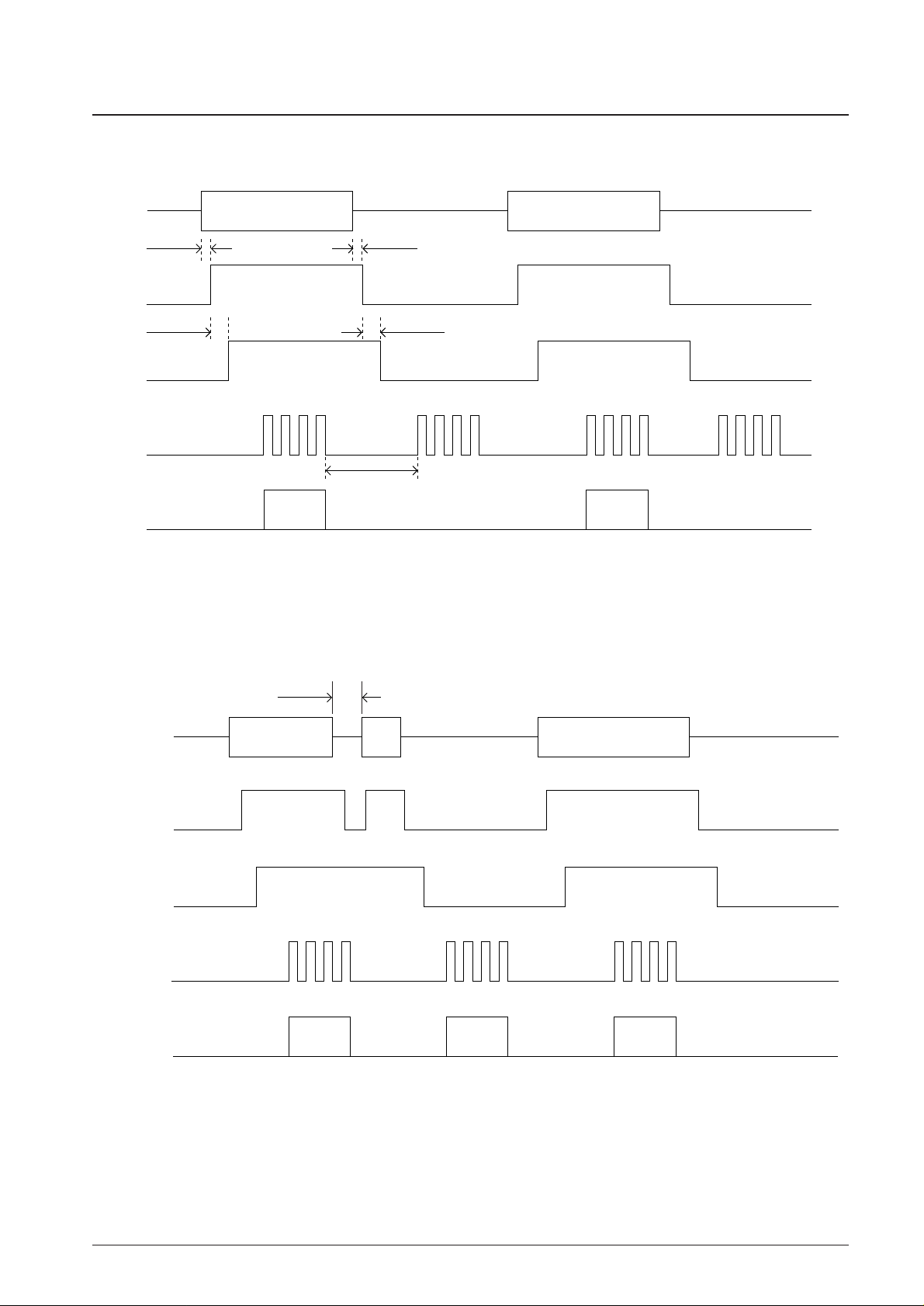
Timing Chart (DTMF mode)
Timing chart for the normal state (when DTMF signal #n and #n+1 have been input.)
When a DTMF signal (#n) is separated into two events due to a burst waveform or other problem.
No. 6124-6/17
LC73815M
Page 7

No. 6124-7/17
LC73815M
INPUT
EST
STD
ACK
DATA
#n
#n+α
t
REC
t
REC
#n+1
#n #n+α #n+1
A12314
INPUT
EST
STD
ACK
DATA
#n
t
ID
#n+2#n+1
#n #n+2
A12315
LSB MSB LSB MSB
When a pseudo-DTMF signal consisting of noise (#n + α) is input.
When the output data is incorrect due to displacement of the input clock
Note: The output data is output from the DATA pin in response to four pulses applied as a set to the ACK pin. The output data are composed of four ACK
pulses.There must be a wait time of at least 20 µs between the last of these 4 ACK pulses and the next ACK pulse.
Page 8

No. 6124-8/17
LC73815M
DR
b7
RDO
Parity Start
Stop
ACK
RDO P STOP
t
SDATA
t
SDR
RDO
DATA
ACK
DR
DATA
ACK
START b1 b2
b6b5 b7 P
b1 b2
DATA
A12316
P 1 0 b1 b2
b2b1
b3 b4 b5 b6 b7 P 1 0 b1 b2 b3 b4 b5 b6 b7 p1
b3 b4 b5 b6 b7 b2b1 b3 b4 b5 b6 b7 PP
t
CKL
t
CKH
f
ACK
t
SCKDR
t
SCKD
Timing Chart (FSK mode reception)
Page 9

No. 6124-9/17
LC73815M
STOP START b1n STOP START b1n+1b2n b3n b4n b5n b6n b7n b2n+1 b3n+1 b3n+1 b4n+1Pn
STOP START STOP STARTb1n b2n b3n b4n b5n b6n b7n Pn
b1n+1 b2n+1 b3n+1 b3n+1 b4n+1 b5n+1
T
DDEM
FSK
RDO
DR
ACK
DATA
FSK
RESET
OSCO
DR
RDO
ACK
b1n-1 b2n-1 b3n-1 b4n-1 b5n-1 b6n-1 b7n-1 Pn-1 b1n b2n b3n b4n b6nb5n
A12317
A12318
01010101010101010101
Channel seizure signal mark signal
1111111111111111111 Message data
0101010101010101---
Invalid data
Message data1111111111111111--- invalid data
Page 10

No. 6124-10/17
LC73815M
S/R
ACK
DATA
DR
FSK
DRCNT
D0 to D7
Idling
Start bit
Start bit
IdlingD0 D1 D2 D3 D4 D5 D6 D7
S/R
ACK
DATA
DR
FSK
DRCNT
A12319
A12320
#1
#1 #2 #3 #4
#2
Start bit
Idling
Stop bit Stop bit Stop bit Stop bit
Start bit
#4#3
Idling
Start bit Start bit
At least 5 bits of idling inserted
Idling
Timing Chart (FSK mode transmission)
Page 11

No. 6124-11/17
LC73815M
S/R
ACK
DATA
DR
DRCNT
D0 to D7
FSK
Start bit
DC bias
Start bit
Idling
D0 D1 D2 D3 D4 D5 D6 D7
A12321
A12322
S/R
ACK
DATA
DR
FSK
DRCNT
#1 #2 #3 #4
Start bit
DC bias
Stop bit Stop bit Stop bit
Stop bit
Idling
Start bit
Idling
Start bit Start bit
At least 5 bits of idling inserted
#1 #2 #3 #4
Page 12

No. 6124-12/17
LC73815M
DR
FSK
DRCNT
Idling
Idling
S/R
A12323
D0 D1 D2 D3 D4 D5 D6 D7 D0 D1 D2 D3 D4 D5 D6 D7
DATA
#1
#2
ACK
DC bias
Idling
Start bit
Start bit
Stop bitStop bit
#1 #2
At least 5 bits of idling inserted
DR
FSK
DRCNT
Idling
Idling
S/R
A12324
D0 D1 D2 D3 D4 D5 D6 D7 D0 D1 D2 D3 D4 D5 D6 D7
DATA
#1
#2
ACK
DC bias
Idling
Start bit
DC bias
Idling
Start bitStop bit
Stop bit
#1 #2
At least 5 bits of idling inserted
Page 13

No. 6124-13/17
LC73815M
Pin Internal Connection
Pin No. Pin Internal connection
1
2
3
IN
+
IN
–
GS
+
–
IN
–
IN
+
V
DD
V
DD
V
DD
GS
A12325
3
2
1
4
10
AGNDI
AGNDO
+
–
V
DD
V
DD
V
DD
AGNDI
AGNDO
A12326
10
4
6 FSKOUT
V
DD
V
DD
FSKOUT
A12327
6
7
8
AGCO
FSKIN
+
–
V
DD
+
–
1/2V
DD
V
DD
AGCO
FSKIN
A12328
7
8
12
13
21
22
TESTI
B/V
S/R
F/D
V
DD
A12329
13
12
21
22
B/V
TESTI
S/R
F/D
Continued on next page.
Page 14

No. 6124-14/17
LC73815M
Continued from preceding page.
Pin No. Pin Internal connection
15
16
OSCIN
OSCOUT
V
DD
V
DD
OSCIN
SOCOUT
A12330
16
15
24 DATA
DATA
V
DD
V
DD
V
DD
A12331
24
25
29
ACK
RES
V
DD
A12332
29
25
RES
ACK
30 DRCNT
DRCNT
V
DD
A1233
30
26
27
31
34
EST/DR
STD/DR
TESTO1
TESTO2
EST/DR
STD/DR
TESTO1
TESTO2
V
DD
V
DD
A12334
27
26
31
34
Page 15

Pin Assignment
No. 6124-15/17
LC73815M
18
17
16
15
14
13
12
11
10
9
8
7
6
5
4
3
2
1
19
20
21
22
23
24
25
26
27
28
29
30
31
32
33
34
35
36
V
DD
NC
S/R
F/D
NC
DATA
ACK
EST/DR
STD/DR
RDO
RES
DRCNT
TESTO1
NC
NC
TESTO2
(I)
(I)
(I/O)
(I)
(O)
(O)
(O)
(I)
(I)
(O)
(O)
NC
NC
V
SS
NC
OSCOUT
OSCIN
NC
B/V
TESTI
NC
AGND
NC
FSKIN
AGCO
FSKOUT
NC
AGND
GS
IN
–
IN
+
(I)
(I)
(I)
(I)
(O)
(O)
(O)
(O)
(I)
(I)
LC73815M
Top view
A12335
Page 16

No. 6124-16/17
LC73815M
18
17
16
15
14
13
12
11
10
9
8
7
6
5
4
3
2
1
V
SS
NC
OSCOUT
OSCIN
NC
B/V
TESTI
NC
AGNDI
NC
FSKIN
AGCO
FSKOUT
NC
AGNDO
GS
IN
–
IN
+
V
DD
NC
S/R
F/D
NC
DATA
ACK
EST/DR
STD/DR
RDO
RES
DRCNT
TESTO1
NC
NC
TESTO2
NC
NC
19
20
21
22
23
24
25
26
27
28
29
30
31
32
33
34
35
36
0.1 µF
10 µF
Power supply: 5 V
CPU
Reset (negative logic)
DTMF detection
Clock
Data
FSK/DTMF
switching
0.1 µF
0.1 µF
0.1 µF
DTMF IN
FSK OUT
10 kΩ
33 kΩ
100 kΩ
100 kΩ
A12336
Top view
Sample Application Circuit
This example uses the DTMF receiver and the V.23 modulator, but does not use the FSK demodulator.
Page 17

PS No. 6124-17/17
LC73815M
This catalog provides information as of December, 2000. Specifications and information herein are
subject to change without notice.
Specifications of any and all SANYO products described or contained herein stipulate the performance,
characteristics, and functions of the described products in the independent state, and are not guarantees
of the performance, characteristics, and functions of the described products as mounted in the customer’s
products or equipment. To verify symptoms and states that cannot be evaluated in an independent device,
the customer should always evaluate and test devices mounted in the customer’s products or equipment.
SANYO Electric Co., Ltd. strives to supply high-quality high-reliability products. However, any and all
semiconductor products fail with some probability. It is possible that these probabilistic failures could
give rise to accidents or events that could endanger human lives, that could give rise to smoke or fire,
or that could cause damage to other property. When designing equipment, adopt safety measures so
that these kinds of accidents or events cannot occur. Such measures include but are not limited to protective
circuits and error prevention circuits for safe design, redundant design, and structural design.
In the event that any or all SANYO products (including technical data, services) described or contained
herein are controlled under any of applicable local export control laws and regulations, such products must
not be exported without obtaining the export license from the authorities concerned in accordance with the
above law.
No part of this publication may be reproduced or transmitted in any form or by any means, electronic or
mechanical, including photocopying and recording, or any information storage or retrieval system,
or otherwise, without the prior written permission of SANYO Electric Co., Ltd.
Any and all information described or contained herein are subject to change without notice due to
product/technology improvement, etc. When designing equipment, refer to the “Delivery Specification”
for the SANYO product that you intend to use.
Information (including circuit diagrams and circuit parameters) herein is for example only; it is not
guaranteed for volume production. SANYO believes information herein is accurate and reliable, but
no guarantees are made or implied regarding its use or any infringements of intellectual property rights
or other rights of third parties.
 Loading...