

SANYO LC4120NV Datasheet
Overview
The LC4120NV is an LCD power supply switching IC
that provides 3 input channels and 6 output channels. It is
fabricated in an 80-V high-voltage CMOS process and
features low power dissipation, high speed, and a low
output impedance. This IC is optimal for switching the
row driver LCD drive voltage in a wide range of LCD
products.
Features
• 3 input channels/6 output channels
• Logic voltage: 2.7 to 5.5 V
• Output voltage: 80 V (maximum)
• Output impedance: 110Ω (maximum)
(When VHA– VLA= 60 V)
• Output delay time: 0.5 µs (maximum)
• Operating temperature: –20 to 75°C
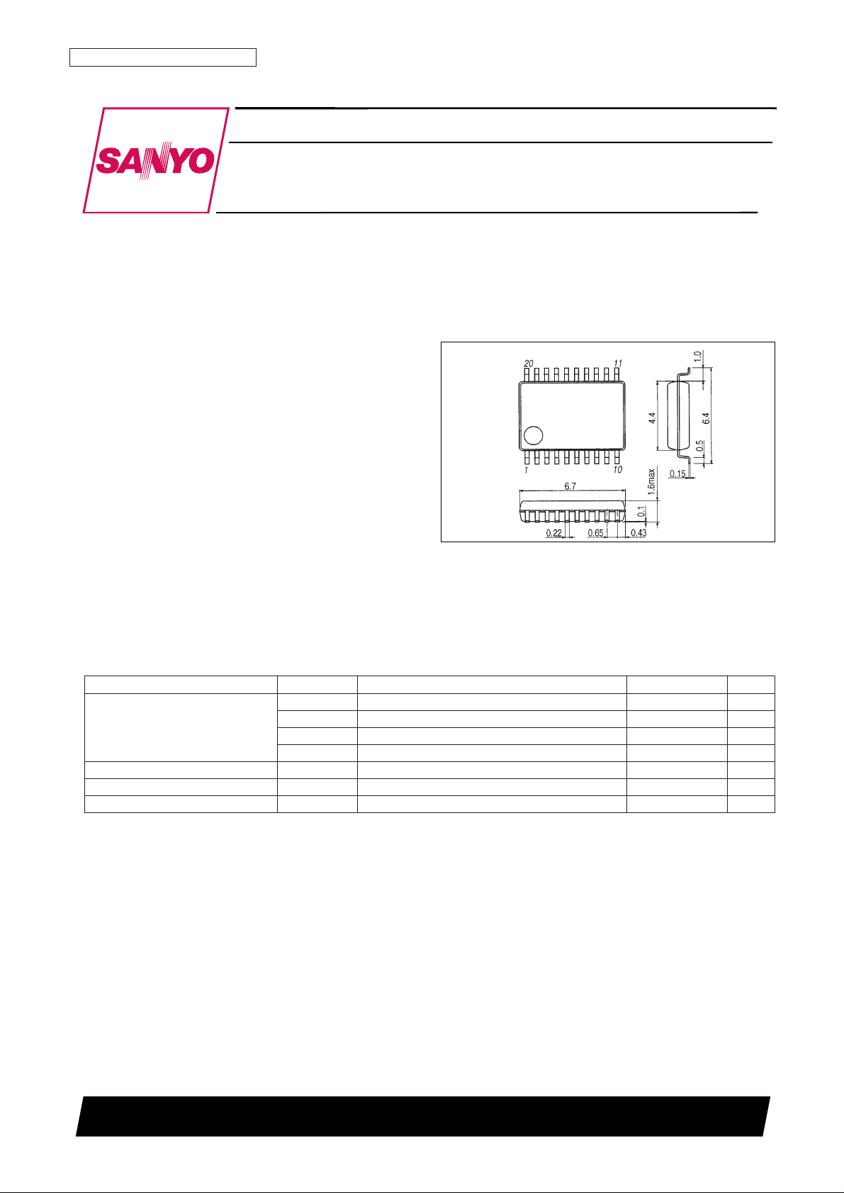
• Package: 20-pin SSOP
Package Dimensions
unit: mm
3179A-SSOP20
CMOS IC
31398HA (OT) No. 5912-1/4
SANYO: SSOP20
[LC4120NV]
SANYO Electric Co.,Ltd. Semiconductor Bussiness Headquarters
TOKYO OFFICE Tokyo Bldg., 1-10, 1 Chome, Ueno, Taito-ku, TOKYO, 110-8534 JAPAN
LCD Power Supply Switching IC
LC4120NV
Ordering number : EN5912
Parameter Symbol Conditions Ratings Unit
V
DD
max V
DD
–0.3 to +7.0 V
Maximum supply voltage
V
HA, B–VLA, BVHA, B/VLA, B
–0.3 to +85 V
V
HA/VHB
VHA/V
HB
–0.3 to +45.0 V
V
LA/VLB
VLA/V
LB
–40.0 to +0.3 V
Input voltage V
IN
S1 to S3 –0.3 to VDD+0.3 V
Operating temperature Topr –20 to +75 °C
Storage temperature Tstg –40 to +125 °C
Specifications
Absolute Maximum Ratings (
The following conditions must hold at all times: VHA≥ VHB> VDD> VSS> VLB≥ VLA)
No. 5912-2/4
LC4120NV
Parameter Symbol Conditions
Ratings
Unit
min typ max
V
DD
V
DD
2.7 5.0 5.5 V
Operating voltage
V
HA, B–VLA, BVHA, B
, V
LA, B
40.0 80.0 V
V
HA
, V
HB
VHA, V
HB
20.0 42.5 V
V
LA
, V
LB
VLA, V
LB
–37.5 –20.0 V
Potential difference
V
HA–VHB
VHA, V
HB
0 5.0 V
V
LA–VLB
VLA, V
LB
0 5.0 V
Input high-level voltage V
IH
S1 to S3 VDD× 0.8 V
DD
V
Input low-level voltage V
IL
S1 to S3 0 VDD× 0.2 V
Output high-level voltage
R
OHA
V
OUT
= VHA– 0.5 : VH1 to VH3 *1 70 110 Ω
R
OHB
V
OUT
= VHB– 0.5 : VH1 to VH3 *1 70 110 Ω
Output low-level voltage
R
OLA
V
OUT
= VLA+ 0.5 : VL1 to VL3 *2 70 110 Ω
R
OLB
V
OUT
= VLB+ 0.5 : VL1 to VL3 *2 70 110 Ω
I
DDOPE
f = 40 kHz, Input signals operating *3 80 µA
Current drain I
HOPE
f = 40 kHz, Input signals operating *3 600 µA
I
HLEAK
f = 40 kHz, Input signals stopped *3 –10 +10 µA
Electrical Characteristics
DC Characteristics at Ta = –20 to 75°C, VSS= 0 V, VDD= 2.7 to 5.5 V unless otherwise specified
(The following conditions must hold at all times: VHA≥ VHB> VDD> VSS> VLB≥ VLA.)
Notes: 1. VHA– VLA= 60 V, VHA– VHB= 1.0 V
2. V
HA
– VLA= 60 V, VLA– VLB= 1.0 V
3. V
HA
– VLA= 60 V, VHA– VHB= VLA– VLB= 1.0 V
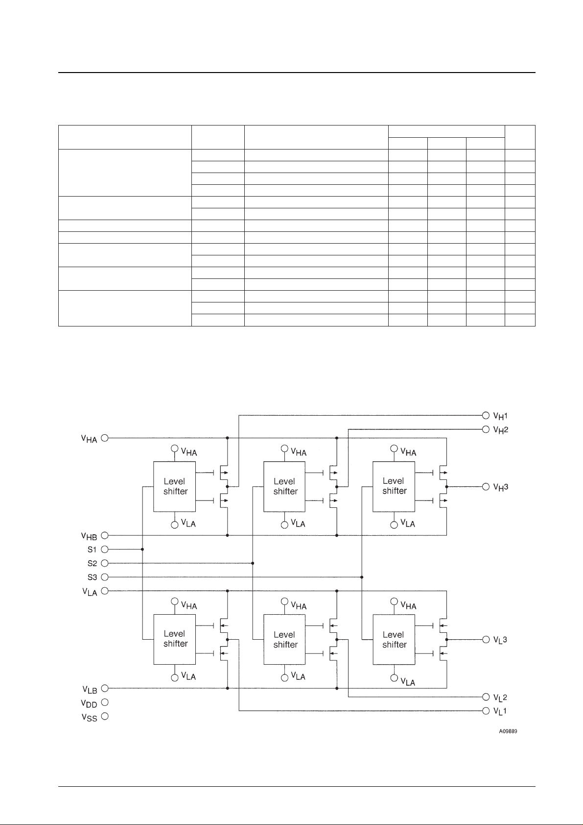
Block Diagram
 Loading...