

SANYO LC4105V Datasheet

Overview
The LC4105V is a level shifter driver that converts 5-V
signals into signals with amplitudes between 10 and 18 V.
Features
• Seven inputs and eleven outputs
IN1 to IN3 produce only true outputs.
IN4 to IN7 produce both true and inverted outputs.
• Slim SSOP-30 package
Package Dimensions
unit: mm
3191-SSOP30
CMOS LSI
43098HA(OT)/13097HA(OT) No. 5641-1/6
SANYO: SSOP30
[LC4105V]
SANYO Electric Co.,Ltd. Semiconductor Bussiness Headquarters
TOKYO OFFICE Tokyo Bldg., 1-10, 1 Chome, Ueno, Taito-ku, TOKYO, 110-8534 JAPAN
Level Shifter
LC4105V
Ordering number : EN5641A
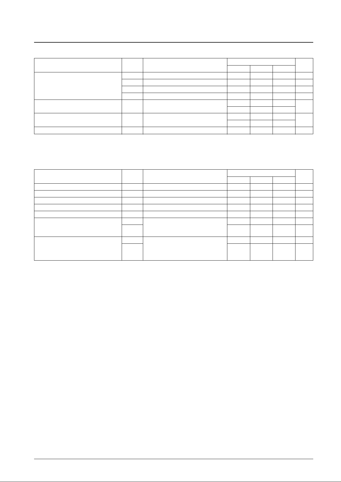
Specifications
Absolute Maximum Ratings at Ta = 25°C ± 2°C, all voltages are relative to VSS, unless otherwise specified
Parameter Symbol Conditions
Ratings
Unit
min typ max
V
DD
–0.3 20 V
Power supply voltage
V
DD
1 –0.3 20 V
V
CC
–0.3 7 V
V
SS
1 –0.3 +0.3 V
Input voltage V
IN
IN1 to IN7 –0.5 VCC+0.5 V
Power dissipation Pd Ta ≤ 75°C 200 mW
Storage temperature Tstg –55 +125 °C
No. 5641-2/6
LC4105V
Parameter Symbol Conditions
Ratings
Unit
min typ max
V
DD
* 10 18 V
Power supply voltage
V
DD
1 * V
DD
V
V
CC
* 3.0 5.5 V
V
SS
1 * V
SS
V
High-level input voltage V
IN
-H
IN1 to IN7 (VCC= 4.5 to 5.5 V) 2.4 V
CC
V
(V
CC
= 3.0 to 4.5 V)
0.7 V
CC
V
CC
Low-level input voltage VIN-L
IN1 to IN7 (VCC= 4.5 to 5.5 V) 0 0.8
V
(V
CC
= 3.0 to 4.5 V)
0 0.1 V
CC
Operating temperature Topr –10 +75 °C
Allowable Operating Ranges at voltages relative to V
SS
Note: * Applications must observe the directions in the note on page 5 at power on and at power off.
Note: * I
DD
I and IDDa are the total currents flowing into power supply pins VDDand VDD1.
Parameter Symbol Conditions
Ratings
Unit
min typ max
High-level input current I
ih
Vin = VCCIN1 to IN7 1 µA
Low-evel input current I
il
Vin = VSSIN1 to IN7 –1 µA
High-level output voltage V
oh
Io = 1 mA VDD–1 V
DD
V
Low-level output voltage V
ol
Io = –1 mA V
SS
VSS+1 V
Output on resistance Rout V
DD
= VDD1 = 10 V Io = ±1 mA 60 Ω
Current drain while idling
I
CCI
VDD= VDD1 = 18 V, VCC= 5.5 V 0.01 10 µA
I
DDI
*
IN1 to IN7 = 0 V
0.10 10 µA
. All outputs open.
I
CCa
VDD= VDD1 = 15 V, VCC= 5.5 V
16 µA
Current drain during operation
IN0 to IN6 = 0 V
I
DDa
* IN7 = 0 to 5.5 V/2 MHz 10 mA
Load 1
Electrical Characteristics
at Ta = 25°C ±2°C, VCC= 5 V, and VDD= 16 V, all voltages are relative to VSS, unless othrewise specified
 Loading...