

SANYO LC4100C Datasheet
Overview
The LC4100C is a common driver for large-scale dot
matrix LCD panels. It includes a 240-bit bidirectional shift
register and 4-level LCD driver circuits. The number of
bits can be further increased by using the provided input
and output pins to connect multiple LC4100Cs in cascade.
The LC4100C and LC4101C form a large-screen LCD
panel driver chip set.
Features
• Fabricated in a CMOS (P-sub) high-voltage process.
• LCD drive voltage: 36 V
• Logic system power-supply voltage: 3.0 to 5.5 V
•f
load
max: 1 MHz
• Slim chip (output pads are concentrated on one of the
longer sides)
• 240 outputs (pad pitch: 70 µm)
• Bidirectional shift register
• The shift register can be split into two 120-bit registers.
• DISPOFF function that locks the drive voltages output
to the LCD at fixed levels.
• Display duty: 1/160 to 1/480
CMOS LSI
93096HA (OT)/31596HA (OT) No. 5279-1/8
SANYO Electric Co.,Ltd. Semiconductor Bussiness Headquarters
TOKYO OFFICE Tokyo Bldg., 1-10, 1 Chome, Ueno, Taito-ku, TOKYO, 110 JAPAN
LCD Dot Matrix Common Driver
for STN Displays
LC4100C
Ordering number : EN5279B
Parameter Symbol Conditions Ratings Unit
V
DD
–0.3 to +7 V
Supply voltage V
EEn
–0.3 to +40 V
V
SSn
–0.3 to +0.3 V
V
IN
LOAD, L/R, DISP, DF, EIO1, EIO3, EIO4 –0.3 to VDD+ 0.3 V
Input voltage
V
0
, V
1
VEE– 7 to VDD+ 0.3 V
V
4
–0.3 to VSS+7 V
V
5
–0.3 to +0.3 V
Operating temperature Topr –20 to +75 °C
Storage temperature Tstg –55 to +125 °C
Specifications
Absolute Maximum Ratings at Ta = 25°C ± 2°C, standard VSS, V
EEn
= V
EE1
or V
EE2
, V
SSn
= V
SS1
or V
SS2
Note: The voltages V1, V2, V3, V4, and V5must obey the relationships V
EEn
+ 0.3 ≥ V0≥ V1≥ VEE– 7, and 7 ≥ V4≥ V5≥ V
SSn
– 0.3. (Unit: V)

No. 5279-2/8
LC4100C
Parameter Symbol Conditions
Ratings
Unit
min typ max
V
DD
3.0 5.5 V
Supply voltage V
EEn
20 36 V
V
SSn
0 V
Input high-level voltage V
IH
LOAD, L/R, DISP, DF, EIO1, EIO3, EIO4 0.8 V
DD
V
DD
V
Input low-level voltage V
IL
LOAD, L/R, DISP, DF, EIO1, EIO3, EIO4 0 0.2 V
DD
V
V
0
, V1V0, V
1
V
EEn
– 7 V
EEn
V
Input voltage V
4
V
4
0 V
EEn
+ 7 V
V
5
V
5
0 V
Clock frequency f
load
LOAD 1 MHz
V
DD
=
High-level clock
t
w (ldh)
LOAD 50 ns
5 V ± 10%
pulse width
EIO input setup time t
su (ei)
LOAD, EIO1, EIO3, EIO4 100 ns
EIO input hold time t
ho (ei)
LOAD, EIO1, EIO3, EIO4 30 ns
Clock frequency f
load
LOAD 200 kHz
V
DD
=
High-level clock
t
w (ldh)
LOAD 120 ns
3 to 4.5 V
pulse width
EIO input setup time t
su (ei)
LOAD, EIO1, EIO3, EIO4 120 ns
EIO input hold time t
ho (ei)
LOAD, EIO1, EIO3, EIO4 40 ns
Allowable Operating Ranges at Ta = –20 to +75°C, standard VSS, V
EEn
= V
EE1
or V
EE2
, V
SSn
= V
SS1
or V
SS2
Parameter Symbol Conditions
Ratings
Unit
min typ max
Input high-level current I
IH
VIN= VDD: LOAD, L/R, DISP, DF, EIO1, EIO3, EIO4 1 µA
Input low-level current I
IL
VIN= VSS: LOAD, L/R, DISP, DF, EIO1, EIO3, EIO4 –1 µA
Output high-level voltage V
OH
IO= –0.4 mA: EIO1, EIO4 0.8 V
DD
V
DD
V
Output low-level voltage V
OL
IO= 0.4 mA: EIO1, EIO4 V
SS
0.2 V
DD
V
V
EE1
, V
EE2
= 20 V, V0= 20 V, V0– V0= 0.5 V,
Output on resistance R
OUT
V1= 20 V, V1– V0= 0.5 V, V4= 0 V, V0– V4= 0.5 V, 0.3 0.6 kΩ
V
5
= 0 V, V0– V5= 0.5 V: OUT1 to OUT240
Current drain (1) I
DD
VDD= 3 to 5.5 V, fcp= 50 kHz, fDF= 100 Hz,
300 µA
with no output load
Current drain (2) I
EE
V
EEn
= 36 V, 1 data shift 750 µA
Electrical Characteristics at Ta = –20 to +75°C, standard VSS, VDD= 3 to 5.5 V
Note: 1. The voltages V1, V2, V3, V4, and V5must obey the relationships V
EEn
≥ V0≥ V1≥ VEE– 7, and 7 ≥ V4≥ V5≥ V
SSn
. (Unit: V)
2. When turning on the power supplies, first turn on the logic system power supply and then turn on the high-voltage system power supply;
alternatively, turn both on at the same time.
When turning off the power supplies, first turn off the high-voltage system power supply and then turn off the logic system power supply;
alternatively, turn both off at the same time.
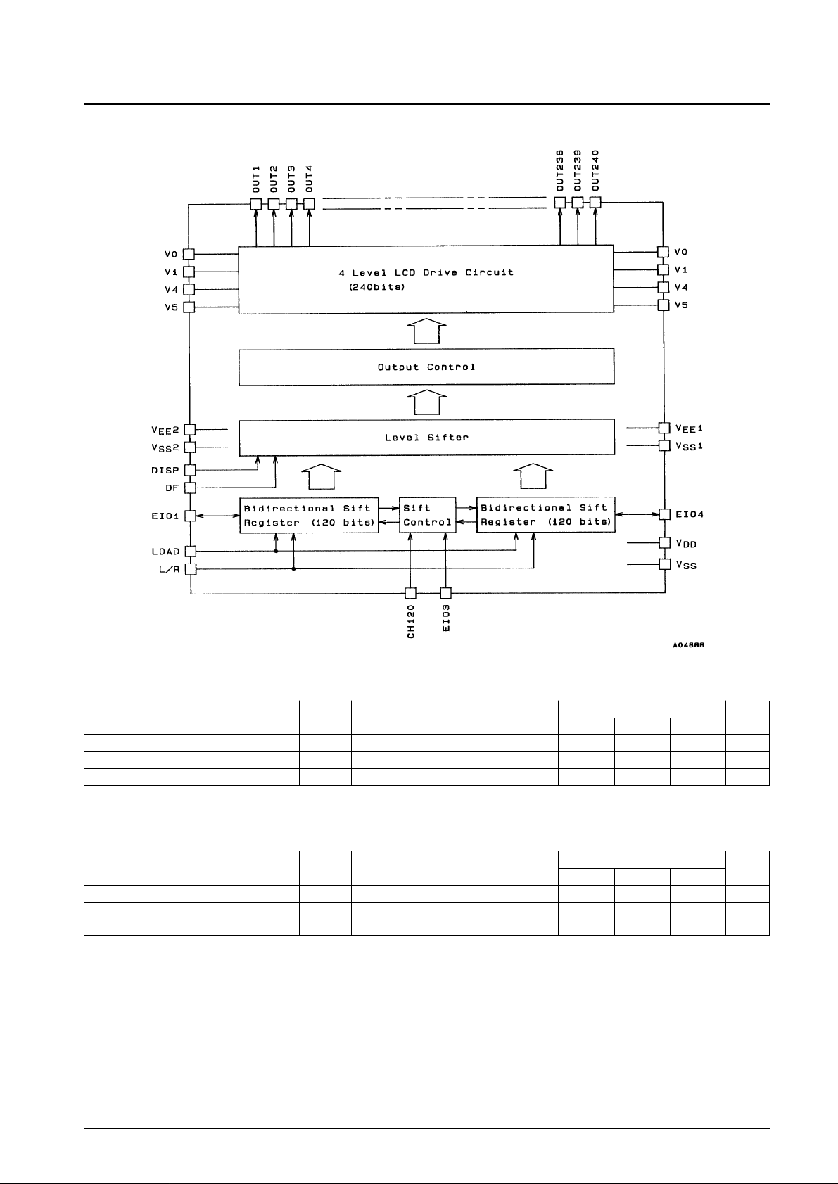
Block Diagram
No. 5279-3/8
LC4100C
Parameter Symbol Conditions
Ratings
Unit
min typ max
EIO output delay time t
d (eo)
30 pF capacitance load: LOAD, EIO1, EIO4 180 ns
LOAD-OUTn delay time t
d (ldo)
100 pF capacitance load: LOAD, OUTn 700 ns
DF-OUTn delay time t
d (dfo)
100 pF capacitance load: DF, OUTn 1.2 µs
Switching Characteristics at VDD= 5 V ± 10%, Ta = –20 to +75°C
Parameter Symbol Conditions
Ratings
Unit
min typ max
EIO output delay time t
d (eo)
30 pF capacitance load: LOAD, EIO1, EIO4 350 ns
LOAD-OUTn delay time t
d (ldo)
100 pF capacitance load: LOAD, OUTn 3 µs
DF-OUTn delay time t
d (dfo)
100 pF capacitance load: DF, OUTn 3 µs
Switching Characteristics at VDD= 3 to 4.5 V, Ta = 25°C ± 2°C
 Loading...