

Overview
The LC374500ST is a 524288-word × 8-bit (4M) mask
programmable ROM that is pin compatible with flash
memory. Since this product supports the wide operating
voltage range of 2.6 to 5.5 V and achieves access times of
100 ns (tCA) when VCCis between 4.5 and 5.5 V and 200
ns when VCCis between 2.6 and 5.5 V, it can be used both
in high-speed 5-V systems and battery-operated 3-V
systems. Since this product is pin compatible with flash
memory it can replace flash memory used during
prototyping and production.
Features
• 524288-word × 8-bit organization
• Wide supply voltage range: 2.6 to 5.5 V
• Access times (tAA): 120 ns (maximum) at VCC= 4.5 to
5.5 V
(tCA): 100 ns (maximum) at VCC= 4.5 to
5.5 V
200 ns (maximum) at VCC= 2.6 to
5.5 V
• Operating supply current: 50 mA (maximum)
• Standby mode supply current: 30 µA (maximum)
• Fully static operation (internal synchronization)
• Three-state outputs
• Pin compatible with flash memory
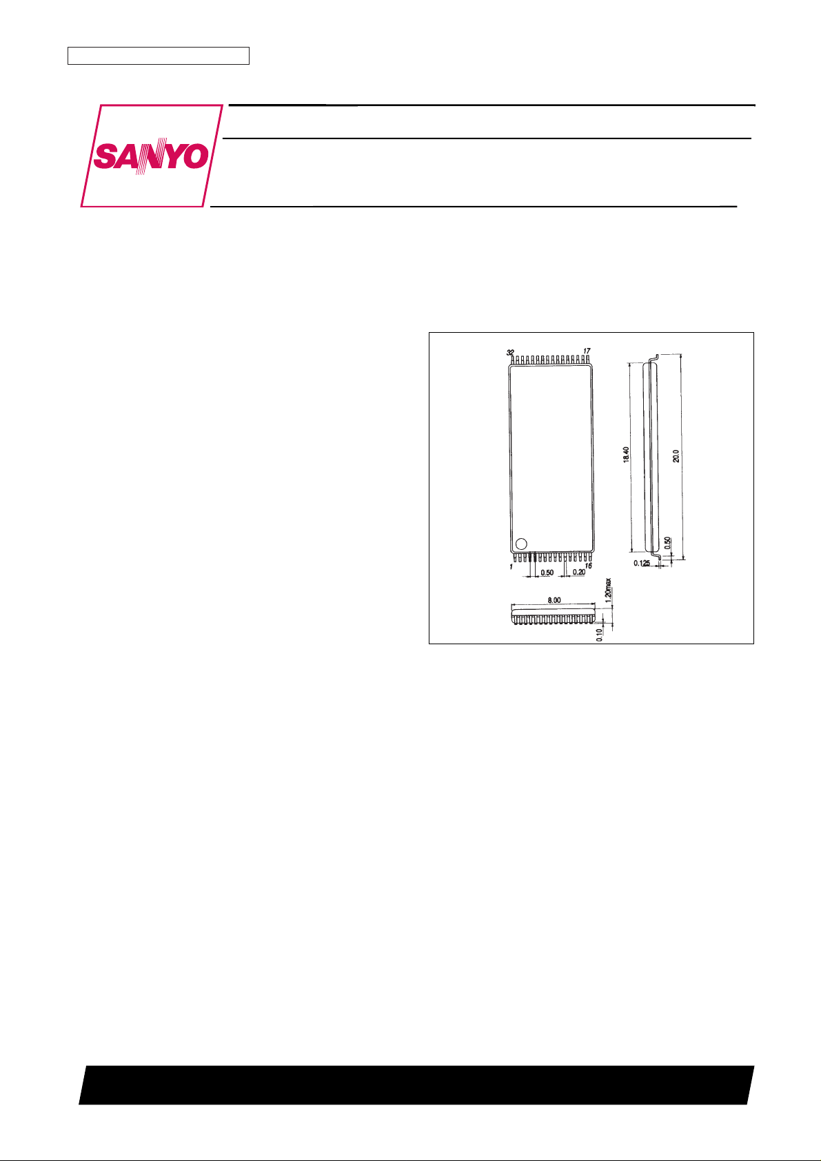
• Package—32-pin TSOP ( 8 × 20 mm) plastic package:
LC374500ST
Package Dimensions
unit: mm
3224-TSOP32
CMOS LSI
22898HA (OT) No. 5610-1/4
Preliminary
SANYO: TSOP32
[LC374500ST]
SANYO Electric Co.,Ltd. Semiconductor Bussiness Headquarters
TOKYO OFFICE Tokyo Bldg., 1-10, 1 Chome, Ueno, Taito-ku, TOKYO, 110-8534 JAPAN
Internal Synchronization Silicon Gate 4M (524288-word
× 8-bit) mask ROM Pin Compatible with Flash Memory
LC374500ST
Ordering number : EN*5610A
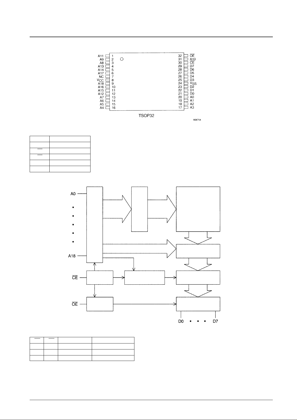
Pin Assignment
No. 5610-2/4
LC374500ST
Block Diagram
Pin Functions
A0 to A18 Address input
Do to D7 Data output
CE Chip enable input
OE Output enable input
V
CC
Power supply
V
SS
Ground
Address buffer
Row decoder
Memory cell array
Column decoder
Sense amplifiers
Output buffer
CE buffer
OE buffer
Internal timing
generator
Function Logic Table
Note: “X” indicates either a high or a low level.
CE OE Output pin state Supply current
H X High-impedance Standby mode current
L H High-impedance Operating mode current
L L DOUT Operating mode current
Top view
 Loading...