

SANYO LB1998 Datasheet
Ordering number : EN5979A
LB1998
Monolithic Digital IC
LB1998
Three-Phase Brushless Motor Driver
for CD-ROM Spindle Drive
Overview
The LB1998 is a three-phase brushless motor driver
especially suited for CD-ROM spindle motor drives.
Functions
• Current linear drive
• Control V type amplifier
• Top side current detection technique reduces loss
voltage of current detection resistor. Voltage effect of
this resistor reduces internal current drain of IC.
• Built-in current limiter circuit
• Built-in reverse blocking circuit
• Hall FG output
• Built-in 1 Hall FG/3 Hall FG switching circuit
• Built-in short braking circuit
• Built-in Hall bias cicuit
• Built-in thermal shutdown circuit
• Built-in S/S function
• Built-in 3 mode gain switching function ensures
compatibility with 8/12 cm CAV and CLV discs
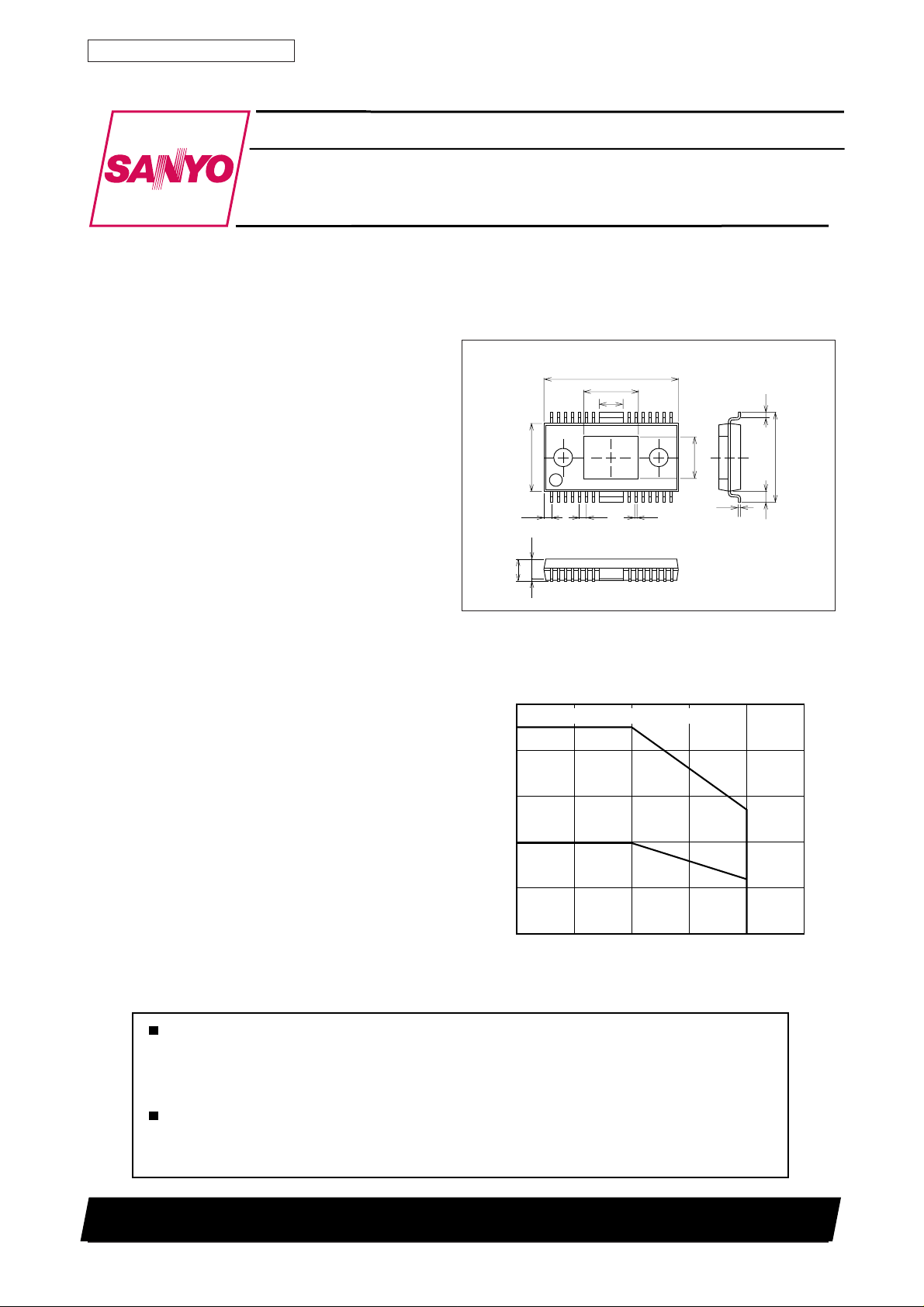
Package Dimensions
unit: mm
3234-HSOP28HC
[LB1998]
15.3
6.2
28 15
7.9
1
0.85
2.25
2.5max
0.1
2.0
With substrate (
1.8
1.6
2.7
0.8
Pd max – Ta
114.3 mm×76.1 mm×1.6 mm3)
0.65
4.9
0.3
0.25
SANYO : HSOP28HC
10.5
1.3
1.2
IC only
0.8
0.4
Allowable power dissipation, Pd max – W
0
Any and all SANYO products described or contained herein do not have specifications that can handle
applications that require extremely high levels of reliability, such as life-support systems, aircraft's
control systems, or other applications whose failure can be reasonably expected to result in serious
physical and/or material damage. Consult with your SANYO representative nearest you before using
any SANYO products described or contained herein in such applications.
SANYO assumes no responsibility for equipment failures that result from using products at values that
exceed, even momentarily, rated values (such as maximum ratings, operating condition ranges, or other
parameters) listed in products specifications of any and all SANYO products described or contained
herein.
0–25 25 50 75 100
Ambient temperature, Ta – °C
0.79
1.08
0.474
SANYO Electric Co.,Ltd. Semiconductor Company
TOKYO OFFICE Tokyo Bldg., 1-10, 1 Chome, Ueno, Taito-ku, TOKYO, 110-8534 JAPAN
60499RM(KI)/30299RM(KI)
No. 5979-1/9
LB1998
Specifications
Maximum Ratings at Ta = 25°C
Parameter Symbol Conditions Ratings Unit
Power supply voltage 7.0 V
Applied output voltage 14.4 V
Applied intput voltage V
Output current 1.3 A
Allowable power dissipation Pd max IC only 0.79 W
Operating temperature Topr –20 to +75 °C
Storage temperature Tstg –55 to +150 °C
Operating Conditions at Ta = 25°C
Parameter Symbol Conditions Ratings Unit
Power supply voltage 4 to 6 V
VCC1 max
VCC2 max
VCC3 max
VO max
VIN max
IO max
VCC1
VCC2
with substrate (114.3 × 76.1 × 1.6 mm3,
glass exposy)
≥VCC1
14.4 V
14.4 V
VCC1
1.80 W
4 to 13.6 V
Sample Application at Ta = 25°C
Parameter Symbol Conditions Ratings Unit
12V type Regulated voltage 4 to 6 V
VCC1
VCC2
Unregulated voltage 4 to 13.6 V
No. 5979-2/9
LB1998
Electrical Characteristics at Ta = 25°C, VCC1 = 5V, VCC2 = 12V
Parameter
[Power supply current]
Power supply current 8 mA
Output idle current 200 µA
[Output]
Saturation voltage, upper side 1 V
Saturation voltage, lower side 1 0.3 V
Current limiter setting voltage 0.25 V
[Hall amplifier]
Common mode input voltage range 1.2 V
Input bias current 1 µA
Minimum Hall input level 60
[S/S pin]
High level voltage 2.0 V
Low level voltage 0.7 V
Input current 200 µA
Leak current –30 µA
[Control]
V
pin input current
CIN
V
pin input current
CREF
Voltage gain 0.25 times
Startup voltage 1.55 1.85 V
Startup voltage width 100 200 mV
[Gain switching amplifier]
Input offset voltage Design target value –8 +8 mV
OPEN LOOP voltage gain f = 10 kHz, Design target value 43 dB
Same-phase input voltage range 0 3.5 V
[Hall power supply]
Hall power supply voltage 0.8 V
Allowable current 20 mA
[Thermal shutdown]
Operating temperature Design target value 150 180 210 °C
Hysterisis Design target value 15 °C
[Short braking]
Brake pin at High level 4 5 V
Brake pin at Low level 0 1 V
[1 Hall FG/3 Hall FG switching]
FG
pin at High level
SEL
FG
pin at Low level
SEL
[Gain switching analog switch]
Analog switch at High level
Analog switch at Low level 0 0.2
Symbol
ICC1
ICC2
ICC1OQ
ICC2OQ
VOU1
VOD1
V
CL
V
HCOM
I
HIB
V
HIN
V
S/SH
V
S/SL
I
S/SI
I
S/SL
I
VC
I
VCREF
GV
CO
V
CTH
∆V
CTH
V
GCOFFSET
G
VGC
V
GCOM
V
H
I
H
T
TSD
∆T
TSD
V
BRH
V
BRL
V
FSH
V
FSL
R
INH
R
INL
V
= V
CIN
V
= V
CIN
V
= 0V
S/S
V
= 0V
S/S
IO = –0.5A, VCC1 = 5V, VCC2 = 12V
IO = 0.5A, VCC1 = 5V, VCC2 = 12V
RRF = 0.25Ω
V
= 5V
S/S
V
= 0V
S/S
V
= V
CIN
CREF
V
= V
CIN
CREF
∆VRF/∆VC, Note 1
V
= 1.65V, Note 1
CREF
V
= 1.65V, Note 1
CREF
IH = 5 mA
Conditions
CREF
CREF
= 1.65V
= 1.65V
Note:
• During S/S OFF (standby), the Hall comparator is at High.
• Gain switching amplifier operated at a factor of 1.
• Design target values are not measured.
Ratings
min typ max
250 300 mA
1.0
VCC1–1.0
Unit
60 µA
mV
VCC1
1 µA
1 µA
4 5
0 1
VCC1VCC–0.5
P-P
No. 5979-3/9
 Loading...