

SANYO LB1991V Datasheet
Overview
The LB1991V is a 3-phase brushless motor driver IC that
is optimal for driving the capstan motor in portable VCR
products.
Functions
• 3-phase full-wave voltage drive technique (120°
voltage-linear technique)
• Torque ripple correction circuit (overlap correction)
• Speed control technique based on motor voltage and
current control.
• Built-in FG comparators
• Built-in thermal shutdown circuit
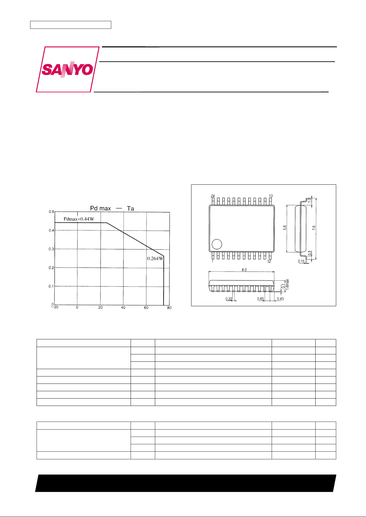
Package Dimensions
unit: mm
3175A-SSOP24
Monolithic Digital IC
53098RM (OT) No. 5792-1/7
SANYO: SSOP24
[LB1991V]
SANYO Electric Co.,Ltd. Semiconductor Bussiness Headquarters
TOKYO OFFICE Tokyo Bldg., 1-10, 1 Chome, Ueno, Taito-ku, TOKYO, 110-8534 JAPAN
Three-Phase Brushless Motor Driver for Portable
VCR Capstan Motors
LB1991V
Ordering number : EN5792
Ambient temperature, Ta — °C
Parameter Symbol Conditions Ratings Unit
V
CC
1 max 10 V
Maximum supply voltage V
CC
2 max 11 V
V
S
max 11 V
Applied output voltage V
O
max VS+ 2 V
Maximum output current I
O
max 1.0 A
Allowable power dissipation Pd max Independent IC 440 mW
Operating temperature Topr –20 to +75 °C
Storage temperature Tstg –55 to +150 °C
Specifications
Absolute Maximum Ratings at Ta = 25°C
Parameter Symbol Conditions Ratings Unit
V
CC
1VCC1 ≤ VCC2 2.7 to 6.0 V
Supply voltage V
CC
2 3.5 to 9.0 V
V
S
Up to VCC2V
Hall input amplitude V
HALL
Between Hall effect element inputs ±20 to ±80 mVp-p
Allowable Operating Ranges at Ta = 25°C
Allowable power dissipation, Pd max — W

No. 5792-2/7
LB1991V
Parameter Symbol Conditions
Ratings
Unit
min typ max
[Supply Current]
V
CC
1 current drain ICC1 I
OUT
= 100 mA 3 5 mA
V
CC
2 current drain ICC2 I
OUT
= 100 mA 7.0 10.0 mA
V
CC
1 quiescent current ICC1Q V
STBY
= 0 V 1.5 3.0 mA
V
CC
2 quiescent current ICC2Q V
STBY
= 0 V 100 µA
VS quiescent current I
S
Q V
STBY
= 0 V 75 100 µA
[VX1]
High side residual voltage V
XH
1 I
OUT
= 0.2 A 0.15 0.22 0.29 V
Low side residual voltage V
XL
1 I
OUT
= 0.2 A 0.15 0.20 0.25 V
[VX2]
High side residual voltage V
XH
2 I
OUT
= 0.5 A 0.25 0.40 V
Low side residual voltage V
XL
2 I
OUT
= 0.5 A 0.25 0.40 V
Output saturation voltage V
O
(sat) I
OUT
= 0.8 A, Sink + Source 1.4 V
Overlap O.L R
L
= 39 Ω × 3, Rangle = 20 kΩ *2 73 80 87 %
High/low overlap difference ∆O.L
(Average high side overlap) –
–8 +8 %
(Average low side overlap) *2
[Hall Amplifiers]
Input offset voltage V
HOFF
*1 –5 +5 mV
Common-mode input voltage range V
HCM
Rangle = 20 kΩ 0.95 2.1 V
I/O voltage gain V
GVH
Rangle = 20 kΩ 25.5 28.5 31.5 dB
[Standby Pin]
High-level voltage V
STH
2.5 V
Low-level voltage V
STL
0.4 V
Input current I
STINVSTBY
= 3 V 25 40 µA
Leakage current I
STLKVSTBY
= 0 V –30 µA
[FRC Pin]
High-level voltage V
FRCH
2.5 V
Low-level voltage V
FRCL
0.4 V
Input current I
FRCINVFRC
= 3 V 20 30 µA
Leakage current I
FRCLKVFRC
= 0 V –30 µA
[VH]
Hall supply voltage V
HALLIH
= 5 mA, VH(+) – VH(–) 0.85 0.95 1.05 V
(–) pin voltage V
H
(–) IH= 5 mA 0.81 0.88 0.95 V
[FG Comparator]
Input offset voltage V
FGOFF
–3 +3 mV
Input bias voltage I
bFG
V
FGIN
+ = V
FGIN
– = 1.5 V 500 nA
Input bias current offset ∆I
bFGVFGIN
+ = V
FGIN
– = 1.5 V –100 +100 nA
Common-mode input voltage range V
FGCM
1.2 2.5 V
Output high-level voltage V
FGOH
At the internal pull-up resistors 2.8 V
Output low-level voltage V
FGOL
At the internal pull-up resistors 0.2 V
Voltage gain V
GFG
*1 100 dB
Output current (sink) I
FGOS
For the output pin low level 5 mA
[TSD]
TSD operating temperature T-TSD Design target value *1 180 °C
TSD temperature hysteresis ∆TSD Design target value *1 20 °C
Electrical Characteristics at Ta = 25°C, VCC1 = 3 V, VCC2 = 4.75 V, VS= 1.5 V
Notes: 1. Items specified as design target values in the conditions column are not tested.
2. The standard for overlap is the value as measured.

Pin Assignment
No. 5792-3/7
LB1991V
Truth Table
Note: The “H” entries in the FRC column indicate a voltage of 2.50 V or higher, and the “L” entries indicate a voltage of 0.4 V or lower. (When VCC1 is 3 V.)
At the Hall inputs, for each phase a high-level input is the state where the (+) input is 0.02 V or higher than the (–) input. Similarly, a low-level input is
the state where the (+) input is 0.02 V or lower than the (–) input.
Source phase → Sink phase Hall input FRC
1
V → W
H H L
H
W → V L
2
U → W
H L L
H
W → U L
3
U → V
H L H
H
V → U L
4
W → V
L L H
H
V → W L
5
W → U
L H H
H
U → W L
6
V → U
L H L
H
U → V L
 Loading...