

SANYO LB1978V Datasheet

Ordering number : EN6186
LB1978V
Monolithic Digital IC
LB1978V
Three-Phase Half-Wave Sensorless Motor Driver
for Headphone Stereos
Functions and Features
• Three-phase sensorless motor driver
• Built-in speed control
• Built-in reference voltage and forward/reverse
switching pin
• Soft switching
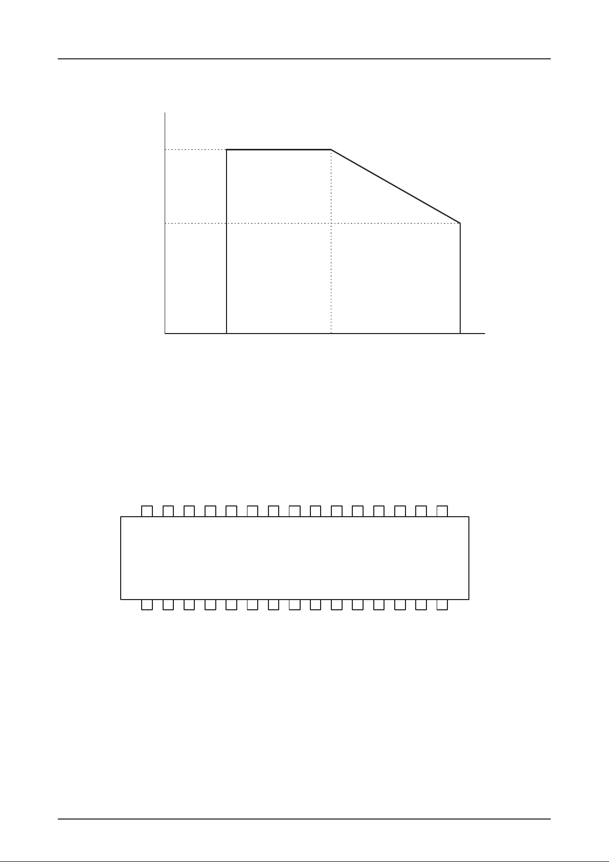
Package Dimensions
unit: mm
3191-SSOP30
[LB1978V]
30
16
1.0
• Built-in short brake drive pin
5.6
115
9.95
0.22
0.65
0.43
0.15
0.1
1.6max
SANYO : SSOP30
7.6
0.5
Specifications
Absolute Maximum Ratings at Ta = 25˚C
Parameter Symbol Conditions Ratings Unit
Maximum supply voltage Vcc max 2.0 V
Output transistor withstand voltage Vsus 4V
Maximum output current Io max 0.6 A
Allowable power dissipation Pd max Tj = 125˚C 0.4 W
Operating temperature Topr 0 to 60 ˚C
Storage temperature Tstg –40 to +125 ˚C
Allowable Operating Ranges at Ta = 25˚C
Parameter Symbol Conditions Ratings Unit
Power supply voltage Vcc 1.0 to 1.7 V
Any and all SANYO products described or contained herein do not have specifications that can handle
applications that require extremely high levels of reliability, such as life-support systems, aircraft's
control systems, or other applications whose failure can be reasonably expected to result in serious
physical and/or material damage. Consult with your SANYO representative nearest you before using
any SANYO products described or contained herein in such applications.
SANYO assumes no responsibility for equipment failures that result from using products at values that
exceed, even momentarily, rated values (such as maximum ratings, operating condition ranges, or other
parameters) listed in products specifications of any and all SANYO products described or contained
herein.
SANYO Electric Co.,Ltd. Semiconductor Company
TOKYO OFFICE Tokyo Bldg., 1-10, 1 Chome, Ueno, Taito-ku, TOKYO, 110-8534 JAPAN
63099RM(KI)
No. 6186-1/9
LB1978V
Electrical Characteristics at Ta = 25˚C, Vcc = 1.2V, in the specified test circuit
Parameter Symbol Conditions
Power supply current Icc START pin H, RIRF = 180 kΩ 6.8 10 mA
START pin L, VBR = 0V 0 10 µA
Reference voltage Vref 0.725 0.755 0.785 V
Reference voltage characteristics ∆Vref
Reference voltage load characteristics
Oscillator cycle T
Rotation switching load characteristics
/ ∆Vcc Vcc = 1.0 to 1.7V 1.0 2.0 %/V
∆Iref
∆Vref
∆Iref
T
Iref = 0 to –50 µA –0.2 –0.06 mV/µA
CS = 1500 pF 0.52 0.6 0.68 ms
S
CS = 1500 pF, 7.70 10.9 ms
F/S
R
= 180 kΩ *Target
IRF
Rotation detection accuracy NF/S TS = 0.60 ms *Target –16 +16 %
COM voltage V
COM
–R
COM
= 1 kΩ 12 25 38 mV
F side output saturation voltage Vsat1 Vcc = 1.0V, Im = 0.3A 0.17 0.30 V
S side output saturation voltage Vsat2 Vcc = 1.0V, Im = 0.2A 0.12 0.25 V
S/S pin input High level voltage V
S/S pin input Low level voltage V
F/S DR pin ON voltage V
F/S DR pin OFF voltage V
SSH
SSL
Lon
Loff
Vcc–0.3 V
TC pin pull-in voltage VTC1 F/S = H 80 110 150 mV
VTC2 F/S = L 160 220 300 mV
BR1 ON voltage V
BR1 OFF voltage V
BRsat voltage V
CI rise voltage V
CI hysteresis width ∆V
IRF voltage V
VI output current I
PV pin voltage V
∆IFC/∆VVI ratio ∆IFC/∆V
Output transistor OFF voltage V
Output transistor ON voltage V
BRon
BRoff
BRsat
OUT
OUT
Io = 6 mA, V
CI
CI
R
IRF
VI
PV
VI
= 180 kΩ 0.725 0.755 0.785 V
IRF
VVI = 0.3V, VIV = GND 26 30 34 µA
= 1.2V 0.15 0.3 V
BR1
OFF Vcc–0.3 V
ON 0.3 V
Note: Items shown to be “Target” are not measured.
Ratings
min typ max
Unit
0.9 V
0.3 V
0.2 V
0.9 V
0.3 V
0.620 0.650 0.680 V
60 80 100 mV
0.720 0.755 0.785 V
150 210 250 µA/V
No. 6186-2/9
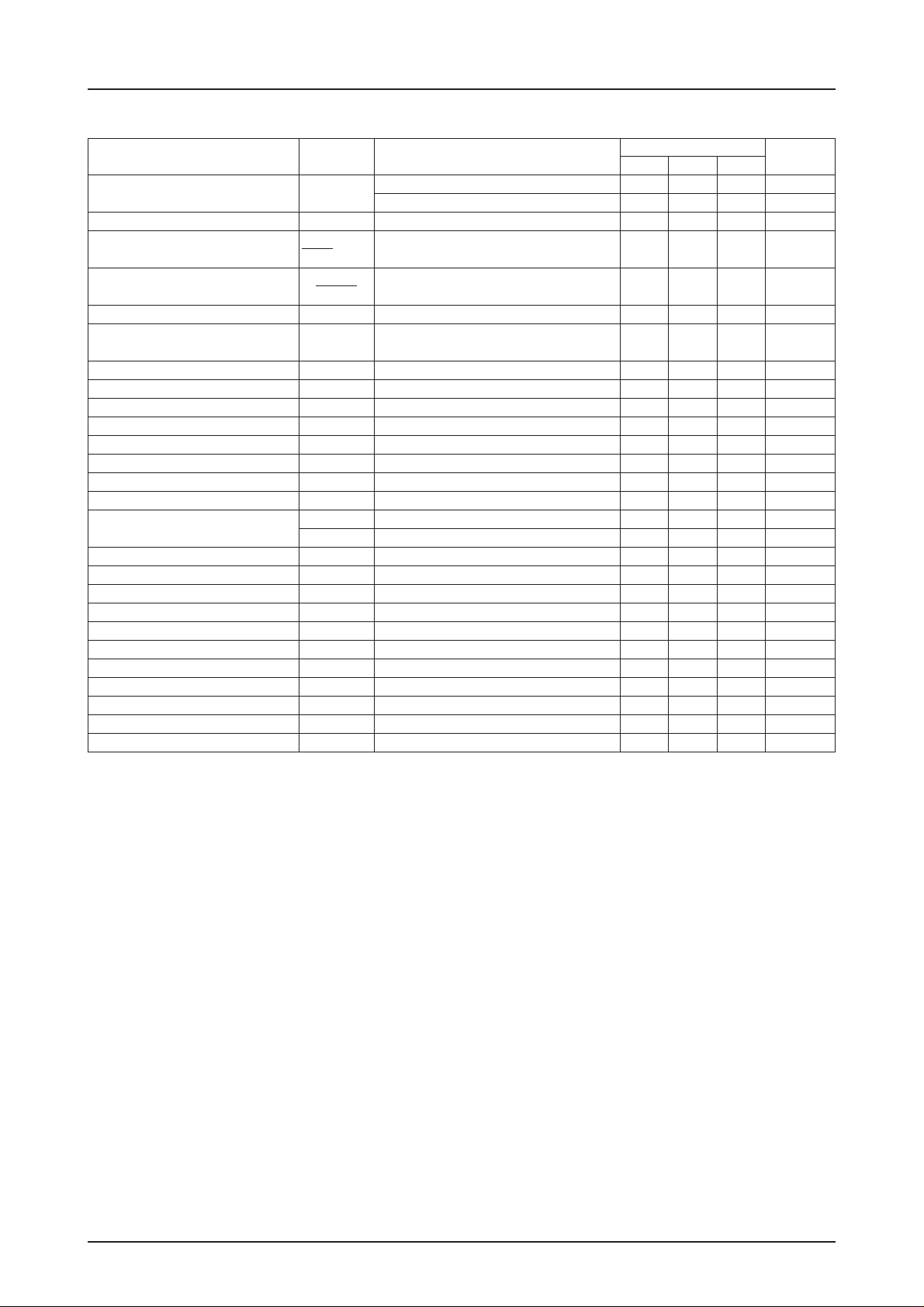
0.4
0.26
Allowable power dissipation, Pd max (W)
025 60
LB1978V
Pd max – Ta
Pin Assignment
Ambient temperature, Ta – (°C)
Vcc
VREF
S/S
DR
F/S
W1
V1
U1
PGNDW2V2
30 2829 27 2526 24 2223 21 1920 18 1617
U2
DU
LB1978V
1 3 2 4 6 5 7 9 8 10 1211 13 1514
IV
FC
OSC
COM
IRF
CI
PW
PV
VI
BR1
BR2
TC1
TC2
SGND
P1
P3
P2
Top view
No. 6186-3/9
 Loading...