

SANYO LB1824 Datasheet
Overview
The LB1824 produces the direct PWM drive output
appropriate for the brushless motors used in office data
processing (OA) equipment, and integrates on a single
chip the speed control circuits, FG amplifier, and other
circuits required to form the drive circuit.
Features
• Breakdown voltage: 30 V, output current: 2.5 A
• Direct PWM drive output
• Crystal oscillator circuit
• Speed discriminator plus PLL speed control system
• Forward/reverse switching circuit
• Start/stop switching circuit
• Current control circuit
• Overheating protection circuit
• Built-in FG amplifier
• Lock detection output
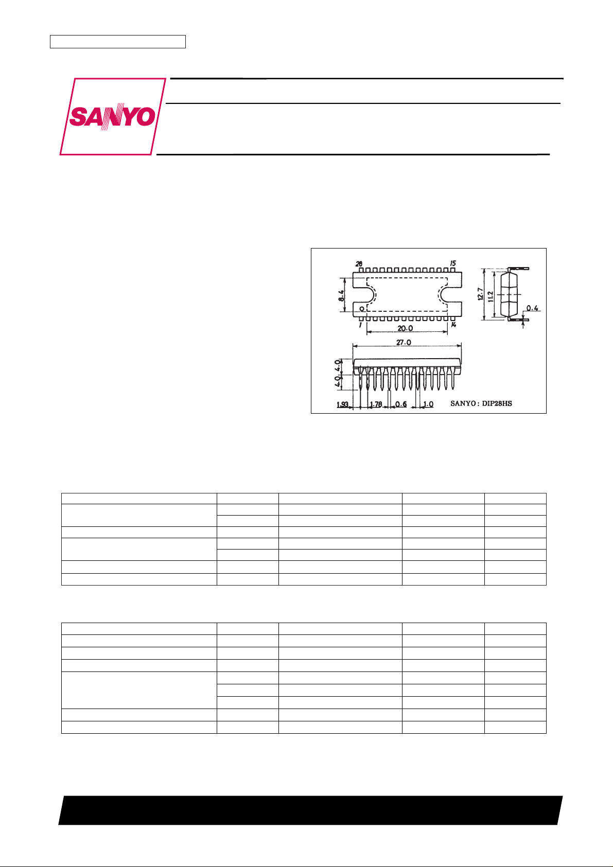
Package Dimensions
unit: mm
3147A-DIP28HS
Specifications
Absolute Maximum Ratings at Ta = 25°C
Parameter Symbol Conditions Ratings Unit
Maximum supply voltage
V
CC
max 30 V
V
M
max 30 V
Output current I
O
max T ≤ 100 ms 2.5 A
Allowable power dissipation
Pd max1 The IC independently 3 W
Pd max2 With an arbitrary large heat sink 20 W
Operating temperature Topr –20 to +80 °C
Storage temperature Tstg –55 to +150 °C
Allowable Operating Ranges at Ta = 25°C
Parameter Symbol Conditions Ratings Unit
Supply voltage range V
CC
9.5 to 28 V
Supply voltage range V
M
9 to 28 V
FG Schmitt output, applied voltage V
FGS
0 to 8 V
I
O1
7 V output 0 to –20 mA
Fixed voltage output current I
O2
5 V output 0 to –20 mA
I
O3
4 V output 0 to –15 mA
FG Schmitt output, output current I
FGS
0 to 5 mA
Lock detection output current I
LD
0 to 20 mA
Monolithic Digital IC
Ordering number : EN4264A
93097HA (OT) / 52893TS A8-8630 No. 4264-1/9
SANYO Electric Co.,Ltd. Semiconductor Bussiness Headquarters
TOKYO OFFICE Tokyo Bldg., 1-10, 1 Chome, Ueno, Taito-ku, TOKYO, 110 JAPAN
Power Brushless Motor Driver
for OA Equipment
LB1824
[LB1824]
Electrical Characteristics at Ta = 25°C, VCC= VM= 24 V
Ratings
Parameter Symbol Conditions
min typ max
Unit
Current drain
I
CC1
34 50 mA
I
CC2
When stopped 8 11 mA
Output saturation voltage
V
Osat1
IO= 1A 2.0 3.0 V
V
Osat2
IO= 2A 2.7 4.2 V
Output leakage current I
Oleak
100 µA
Output voltage V
H
IO= –10 mA 6.65 7.0 7.35 V
7 V fixed voltage output Voltage variation
∆V
H1
VCC= 9.5 to 28 V 50 200 mV
Load variation ∆V
H2
IO= –5 to –20 mA 40 200 mV
Output voltage V
X
IO= –5 mA 4.45 4.80 5.15 V
5 V fixed voltage output Voltage variation ∆V
X1
VCC= 9.5 to 28 V 50 200 mV
Load variation ∆V
X2
IO= –5 to –20 mA 5 200 mV
Output voltage V
FG
IO= –5 mA 3.65 4.0 4.35 V
4 V fixed voltage output Voltage variation ∆V
FG1
V
CC
= 9.5 to 28 V 40 200 mV
Load variation ∆V
FG2
IO= –5 to –15 mA 110 200 mV
Input bias current I
HB
–4 –1 µA
Common mode input voltage range V
ICM
1.5 5.1 V
Hall amplifier
Hall input sensitivity 60 mVp-p
Hysteresis ∆V
IN
8 14 24 mV
Input voltage low → high V
SLH
7 mV
Input voltage high → low V
SHL
–7 mV
Output high level voltage V
OH(CR)
2.8 3.1 3.4 V
Oscillator
Output low level voltage V
OL(CR)
0.8 1.1 1.4 V
Oscillator frequency f
(CR)
R = 56 kΩ, C = 1000 pF 15 kHz
Amplitude V
(CR)
2.0 Vp-p
Current control operation Limiter V
CC –VM
0.4 0.5 0.6 V
Thermal shutdown operation
Thermal shutdown operating temperature
TSD Design target 150 180 °C
Hysteresis ∆TSD 50 °C
Input offset voltage V
IO(FG)
–10 +10 mV
Input bias current I
B(FG)
–1 +1 µA
Output high level voltage V
OH(FG)IFG
= –2 mA 5.5 6 V
FG amplifier
Output low level voltage V
OL(FG)
IFG= 2 mA 1 1.5 V
FG input sensitivity 100x gain 3 mV
Next stage Schmitt width 100 180 250 mV
Operating frequency range 2 kHz
Open loop gain f
(FG)
= 2 kHz 45 51 dB
FGS output
Output saturation voltage V
O(FGS)
I
O(FGS)
= 2 mA 0.1 0.5 V
Output leakage current I
L(FGS)
VO= 5 V 10 µA
Output high level voltage V
OH(D)
4.0 4.3 V
Speed discriminator Output low level voltage I
OL(D)
0.8 1.1 V
Number of counts 512
PLL output
Output high level voltage V
OH(P)
3.2 3.5 3.8 V
Output low level voltage V
OL(P)
1.2 1.5 1.8 V
Lock detection
Output low level voltage V
OL(LD)
ILD= 10 mA 0.15 0.5 V
Locking range ±6.25 %
Input bias current I
B(INT)
–0.4 +0.4 µA
Output high level voltage V
OH(INT)
3.7 4.3 V
Integrator
Output low level voltage V
OL(INT)
0.8 1.2 V
Open loop gain 60 dB
Gain-bandwidth product 1.6 MHz
Reference voltage –5% V
X
/2 5% V
Crystal oscillator Operating frequency range f
OSC
1 10 MHz
Input high level voltage V
IH(S/S)
4.0 V
Start/stop pin Input low level voltage V
IL(S/S)
1.5 V
Pull-down resistance R
D(S/S)
30 50 70 kΩ
Input high level voltage V
IH(F/R)
4.0 V
Forward/reverse pin
Input low level voltage V
IL(F/R)
1.5 V
Hysteresis ∆V
IN
0.5 V
Pull-down resistance R
D(F/R)
30 50 70 kΩ
LB1824
No. 4264-2/9
LB1824
No. 4264-3/9
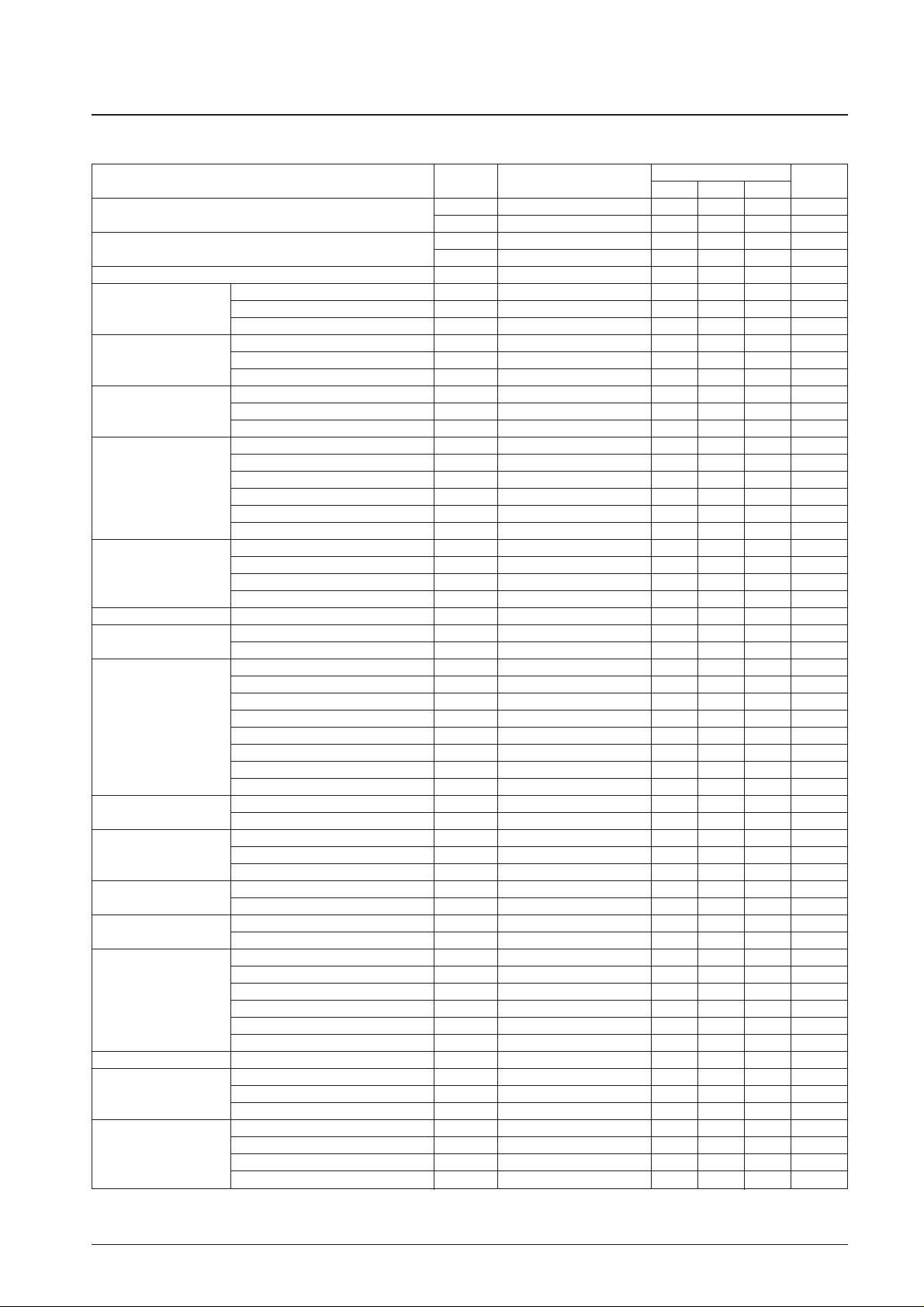
Pd max – Ta
Ambient temperature Ta – °C
Allowable power dissipation, Pd max – W
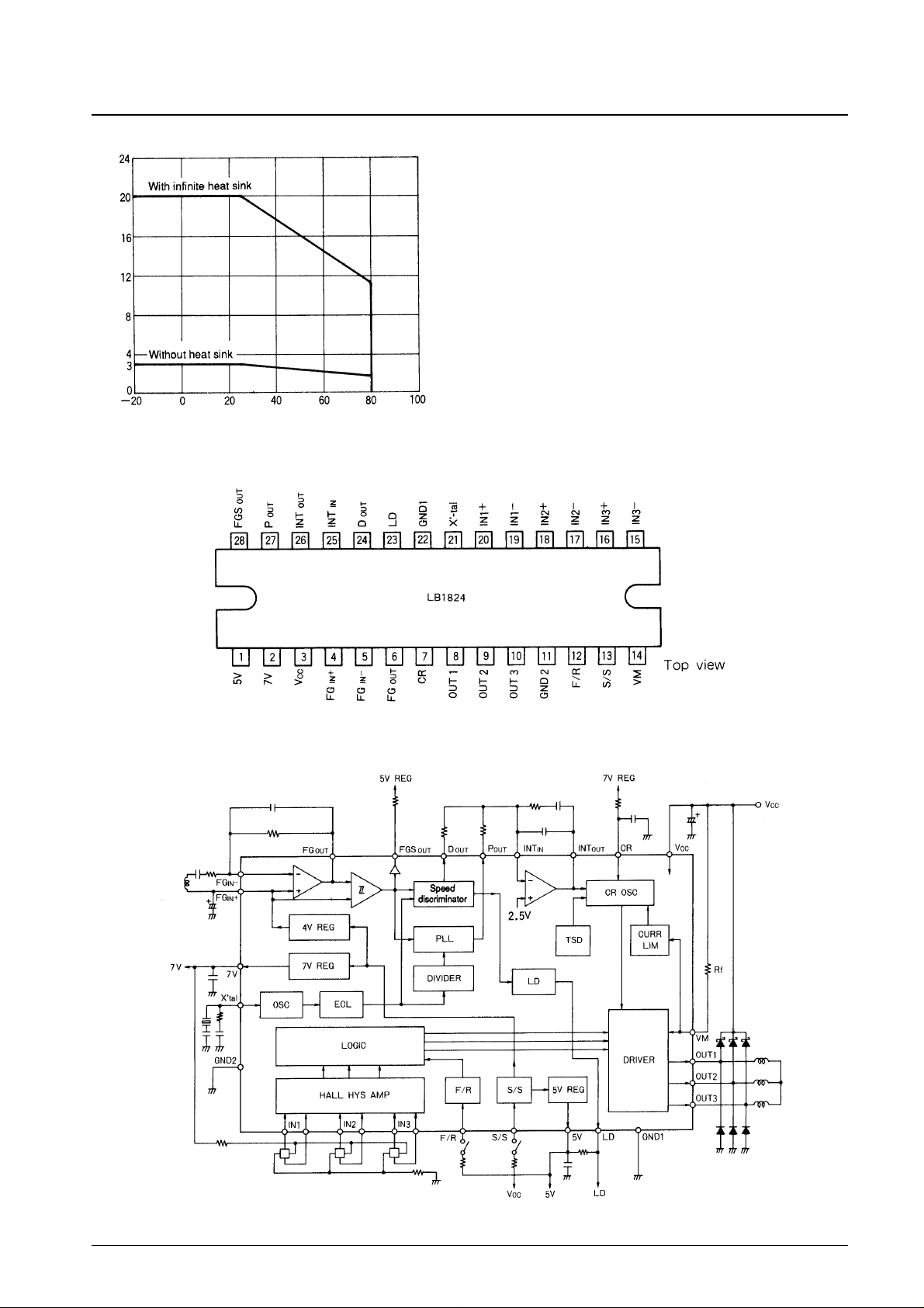
Pin Assignment
Equivalent Circuit Block Diagram
 Loading...