

SANYO LB1823M Datasheet

Ordering number : EN4696B
13097HA(OT)/83095HA (OT) No. 4696-1/11
SANYO Electric Co.,Ltd. Semiconductor Bussiness Headquarters
TOKYO OFFICE Tokyo Bldg., 1-10, 1 Chome, Ueno, Taito-ku, TOKYO, 110 JAPAN
Monolithic Digital IC
LB1823M
SANYO Electric Co.,Ltd. Semiconductor Bussiness Headquarters
TOKYO OFFICE Tokyo Bldg., 1-10, 1 Chome, Ueno, Taito-ku, TOKYO, 110 JAPAN
Power Brushless Motor Predriver IC
for OA Applications
Overview
The LB1823M is a predriver IC developed for driving
power brushless motors in office automation applications.
A motor driver circuit with the desired output power
(current and voltage) can be constructed by attaching
either a driver array or discrete components at the output.
The LB1823M output supports direct PWM drive and thus
allows the implementation of low-loss drive circuits.
Additionally, the LB1823M includes several associated
circuits, such as a speed control circuit, and FG amplifier,
and an integrating amplifier, on chip.
Features
• Direct PWM drive output
• Crystal oscillator circuit
• Speed discriminator plus PLL speed control system
• Lock detector output
• Forward/reverse switching circuit
• Braking circuit (short braking technique)
• Start/stop switching circuit
• Over current limiter circuit (OCL)
• Thermal shutdown circuit (TSD)
• Built-in FG amplifier, integrating amplifier
• Shunt regulator output (7.0 V)
Package Dimensions
unit: mm
3073A-MFP30SD
∏SANYO: MFP30SD
[LB1823M]
Specifications
Absolute Maximum Ratings at Ta = 25°C
Allowable Operating Ranges at Ta = 25°C
Electrical Characteristics at Ta = 25°C, VCC= 6.3 V
No. 4696-2/11
LB1823M
Parameter Symbol Conditions Ratings Unit
Maximum supply voltage V
CC
max 9 V
Maximum input current I
REG
V
REG
pin 10 mA
Output current I
O
UL, VL and WL outputs 30 mA
Allowable power dissipation Pd max 0.9 W
Operating temperature Topr –20 to +80 °C
Storage temperature Tstg –55 to +150 °C
Parameter Symbol Conditions Ratings Unit
Input current range I
REG
V
REG
pin (7 V) 1 to 5 mA
FG Schmitt output applied voltage V
FGS
0 to 8 V
FG Schmitt output current I
FGS
0 to 5 mA
Lock detector output current I
LD
0 to 20 mA
Supply voltage V
CC
4.5 to 7 V
Parameter Symbol Conditions min typ max Unit
Current drain
I
CC
1 33 50 mA
I
CC
2 When stopped 15 25 mA
Output saturation voltage V
O
sat UL, VL and WL outputs: IO= 20 mA 0.2 0.7 V
Output current I
O
UH, VH and WH outputs: V
OUT
= 1.4 V 8 12 16 mA
Output leakage current I
O
leak UL, VL and WL outputs 100 µA
Output off voltage V
O
off UH, VH and WH outputs 0.5 V
[Hall Amplifier]
Input bias current I
HB
–4 –1 µA
Common-mode input
V
ICM
1.5 4.4 V
voltage range
Hall input sensitivity ∆V
IN
60 mVp-p
Hysteresis ∆V
IN
17 32 60 mV
Input voltage low to high V
SLH
16 mV
Input voltage high to low V
SHL
–16 mV
[Oscillator]
Output high level voltage V
OH (CR)
3.1 3.4 3.7 V
Output low level voltage V
OL (CR)
1.2 1.5 1.8 V
Oscillator frequency f
(CR)
R = 56 kΩ, C = 1500 pF 20 kHz
Amplitude V
(CR)
2.0 Vp-p
[Current Limiter Operation]
Limiter V
RF
0.4 0.5 0.6 V
[Thermal Shutdown Operation]
Thermal shutdown operating
TSD Design target 150 180 °C
temperature
Hysteresis ∆TSD Design target 30 °C
[V
REG
Pin]
V
REG
pin voltage V
REG
6.6 7.0 7.3 V
Continued on next page.
Continued from preceding page.
No. 4696-3/11
LB1823M
Parameter Symbol Conditions min typ max Unit
[FG Amplifier]
Input offset voltage V
IO (FG)
–10 +10 mV
Input bias current I
B (FG)
–1 +1 µA
Output high level voltage V
OH (FG)
4.8 5.3 V
Output low level voltage V
OL (FG)
1 1.5 V
FG input sensitivity Gain: 100
× 3 mV
Schmitt amplitude for the
100 180 250 mV
next stage
Operating frequency range 2 kHz
Open-loop gain f
(FG)
= 2 kHz 45 51 dB
[FGS Output]
Output saturation voltage V
O (FGS)IO (FGS)
= 2 mA 0.1 0.5 V
Output leakage current I
L (FGS)VO
= V
CC
10 µA
[Speed Discriminator]
Output high level voltage V
OH (D)
5.3 5.6 V
Output low level voltage V
OL (D)
0.4 1.1 V
[PLL Output]
Output high level voltage V
OH (P)
4.05 4.35 4.65 V
Output low level voltage V
OL (P)
1.85 2.15 2.45 V
Number of counts 512
[Lock Detector]
Output low level voltage V
OL (LD)ILD
= 10 mA 0.1 0.5 V
Output leakage current I
L (LD)
VO= V
CC
10 µA
Lock range ±6.25 %
[Integrator]
Input bias current I
B (INT)
–0.4 +0.4 µA
Output high level voltage V
OH (INT)
5.0 5.6 V
Output low level voltage V
OL (INT)
0.8 1.2 V
Open-loop gain 60 dB
Gain bandwidth product 1.6 MHz
Reference voltage –5% V
CC
/2 5% V
[Crystal Oscillator]
Crystal oscillator frequency f
OSC
Crystal oscillator 1 10 MHz
External input frequency f
CLK
External signal input 1 10.2 MHz
[S/S Pin]
Input high level voltage V
IH (S/S)
4.0 3.05 V
Input low level voltage V
IL (S/S)
2.60 1.5 V
Hysteresis ∆V
IN
0.45 V
Pull-up resistor R
U (S/S)
63 kΩ
[F/R Pin]
Input high level voltage V
IH (F/R)
4.0 3.05 V
Input low level voltage V
IL (F/R)
2.60 1.5 V
Hysteresis ∆V
IN
0.45 V
Pull-down resistor R
D (F/R)
30 50 70 kΩ
[BR Pin]
Input high level voltage V
IH (BR)
4.0 3.05 V
Input low level voltage V
IL (BR)
2.60 1.5 V
Hysteresis ∆V
IN
0.45 V
Pull-down resistor R
D (BR)
30 50 70 kΩ
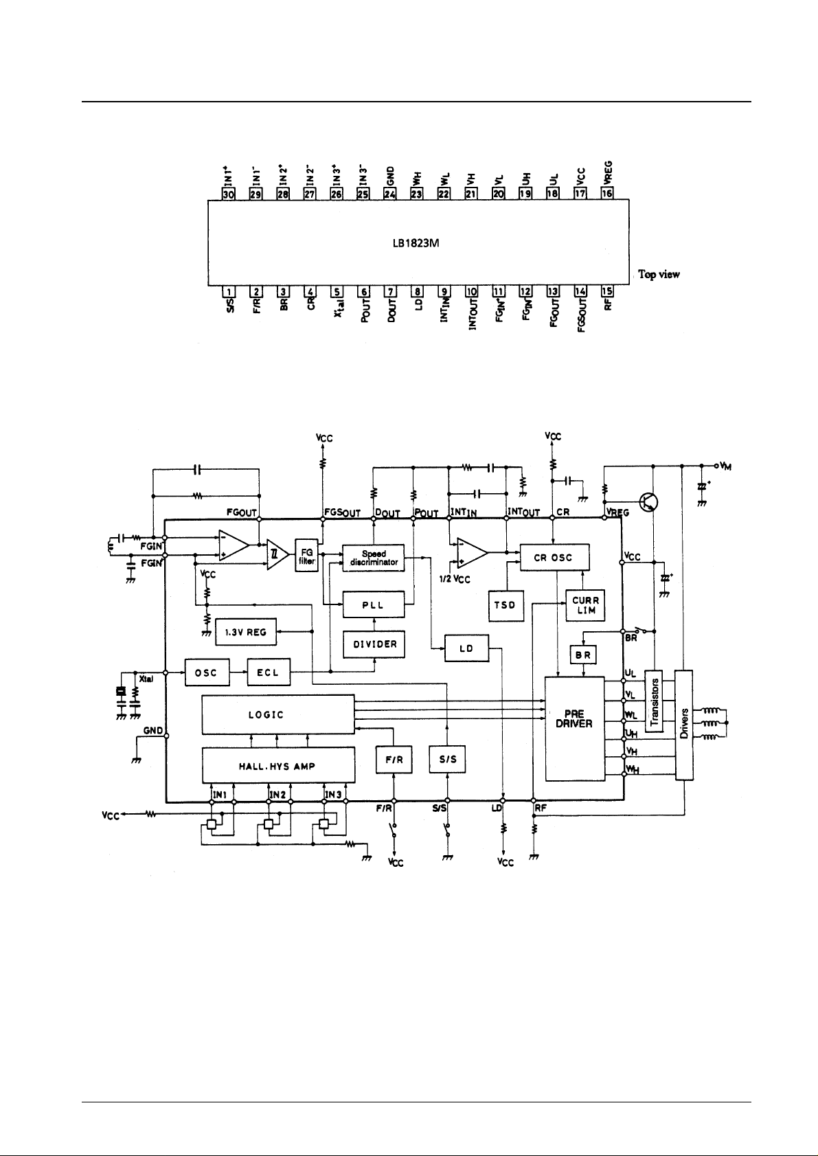
Pin Assignment
Block Diagram
No. 4696-4/11
LB1823M
 Loading...