

SANYO LB1820 Datasheet
Ordering number: EN3302A
Monolithic Digital IC
LB1820
Office Automation-Use 3-Phase Brushless Motor
Driver
Overview
The LB1820 is a three-phase brushless motor with a digital
speed control circuit built in.
The LB1820 is ideally suited for use in office automation
applications such as laser beam printers and drum motor
drivers.
Features
.
Three-phase brushless motor driver with digital speed control
function
.
30 V withstand voltage and 2.5 A output current
.
Current limiter built in
.
Low-voltage protection circuit built in
.
Thermal shutdown circuit built in
.
Hall amp with hysteresis
.
Start/stop pin built in
.
Crystal oscillator and divider built in
.
Digital speed control circuit built in
.
Lock detector built in
Specifications
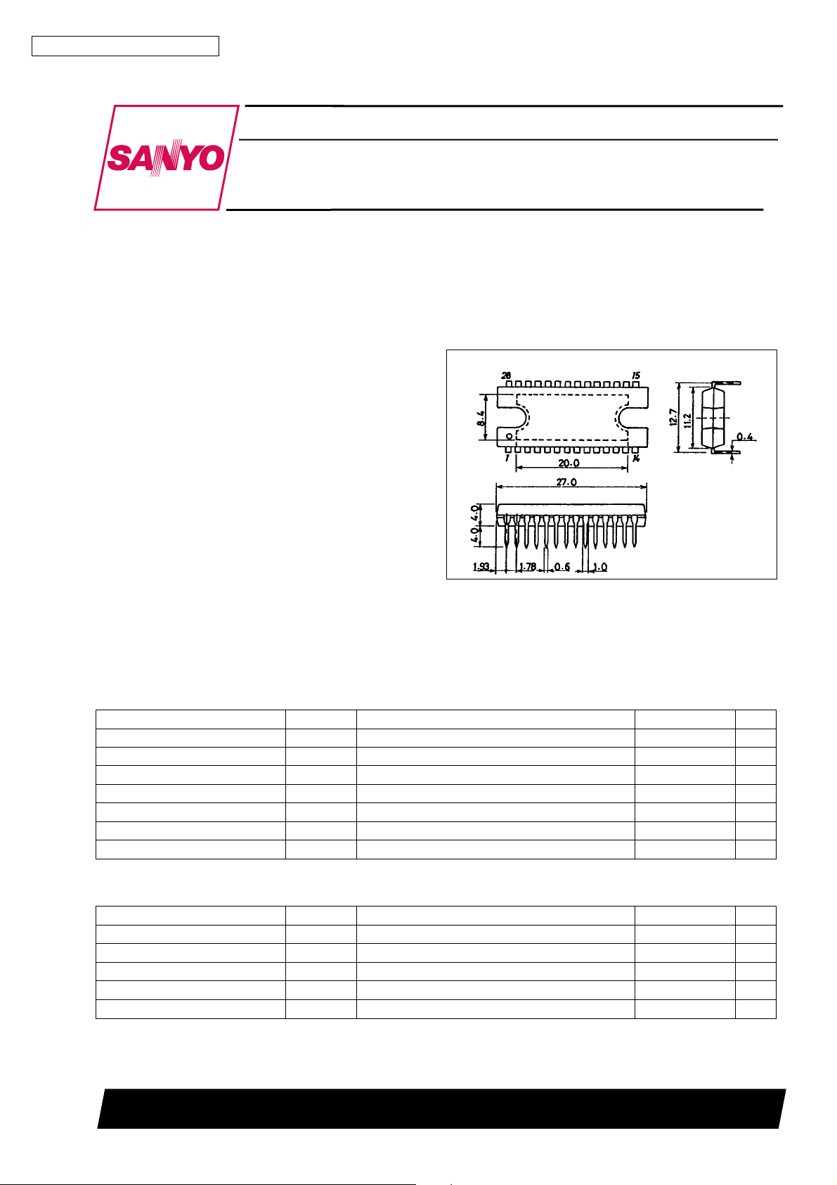
Package Dimensions
unit : mm
3147-DIP28HS
[LB1820]
SANYO : DIP28HS
Absolute Maximum Ratings atTa=25°C
Parameter Symbol Conditions Ratings Unit
Maximum supply voltage 1 V
Maximum supply voltage 2 V
Output current I
Allowable power dissipation 1 Pd max 1 Independent IC 3 W
Allowable power dissipation 2 Pd max 2 With arbitrarily large heat sink 20 W
Operating temperature Topr –20 to +80
Storage temperature Tstg –55 to +150
CC
O
M
t % 100 ms 2.5 A
30 V
30 V
Allowable Operating Ranges atTa=25°C
Parameter Symbol Conditions Ratings Unit
Supply voltage range 1 V
Supply voltage range 2 V
Voltage regulator output current I
Comparator output current I
Lock detector output current I
CC
M
VH
OSC
LD
9.5 to 28 V
5to28 V
0 to +20 mA
0 to +30 mA
0 to +20 mA
C
°
C
°
SANYO Electric Co.,Ltd. Semiconductor Bussiness Headquarters
TOKYO OFFICE Tokyo Bldg., 1-10, 1 Chome, Ueno, Taito-ku, TOKYO, 110 JAPAN
43096HA(II)/3260TA, TS(GTPS) No.3302-1/7
LB1820
Electrical Characteristics atTa=25°C, VCC=VM=24V
Parameter Symbol
Supply current 1 I
Supply current 2 I
Output saturation voltage
V
V
Output leak current I
CC1
CC2
O (sat)
O(sat)
leak 100 µA
O
Stop mode 3 5 mA
1IO= 1 A 2.1 3.0 V
2IO= 2 A 3.0 4.2 V
Conditions
min typ max Unit
33 50 mA
Voltage regulator
Output voltage V
Voltage variation ∆V
Load variation ∆V
IVH= 10 mA 3.8 4.15 4.5 V
H
1VCC= 9.5 to 28 V 60 150 mV
H
2IVH=5to20mA 60 150 mV
H
Temperature coefficient –2 mV/°C
Hall amp
Input bias current I
Common-mode input voltage V
HB
ICM
1.5 2.8 V
14µA
Hall input sensitivity 100 mVp-p
Hysteresis width ∆V
Low-to-high input voltage V
High-to-low input voltage V
IN
SLH
SHL
24 33 42 mV
82032mV
–25 –13 –1 mV
Oscillator
High-level output voltage V
Low-level output voltage V
OH(CR)
OL(CR)
2.9 3.2 3.5 V
0.9 1.1 1.3 V
Oscillation amplitude 1.8 2.1 2.4 V
Oscillation frequency f R = 30 kΩ, C = 1500 pF 18.5 kHz
Temperature coefficient ∆f 0.1 %/°C
Comparator output voltage V
OSC
I
= 20 mA 1.5 V
OSC
Current limiter
Limiter 1 V
Limiter 2 V
1 0.42 0.5 0.6 V
Rf
2 0.4 0.44 0.48 V
Rf
Thermal shutdown
Thermal shutdown
temperature
TSD Design target 150 180
Hysteresis width ∆TSD 30
Low-voltage protection voltage V
Hysteresis width ∆V
LVSD
LVSD
7.5 8.1 8.7 V
0.45 0.6 0.75 V
FG amp
Input offset voltage V
Input bias current I
High-level output voltage V
Low-level output voltage V
IO(FG)
B(FG)
OH(FG)IFG
OL(FG)I(FG)
= –2 mA 5.6 6.2 6.8 V
= 2 mA 1 1.5 V
–10 +10 mV
–1 +1 µA
FG input sensitivity 10 × Gain 5 mV
Schmitt width at next stage 16 mV
Operating frequency range 5 kHz
Open-loop voltage gain 60 dB
Speed discriminator
High-level output voltage V
Low-level output voltage V
OH(D)
OL(D)
4.7 V
0.3 V
Maximum clock frequency 1.0 MHz
Number of counts 2044 2046 2048
Integrator
Input offset voltage V
Input bias current I
High-level output voltage V
Low-level output voltage V
IO(INT)
B(INT)
OH(INT)
OL(INT)
–10 +10 mV
–0.4 +0.4 µA
3.7 4.3 4.9 V
0.8 1.2 V
Open-loop gain 60 dB
Gain-bandwidth product 1.6 MHz
Reference voltage –5% V5/2 5% V
5 V supply V5 4.6 5 5.4 V
C
°
C
°
Continued on next page.
No.3302-2/7

Continued from preceding page.
LB1820
Parameter Symbol
Lock detector
Low-level output voltage V
Lock range ±3.125 %
Start/stop pin
Start/stop operating voltage 0.4 0.5 0.6 V
Crystal Oscillator
Precision of oscillating
frequency
Temperature coefficient –3
Drift in rotational speed ±0.01 %
OL(LD)ILD
=10 mA 0.5 V
Referenced to indicated frequency –500 +500 ppm
Conditions
min typ max Unit
ppm/°C
Truth Table
Source → Sink
1 OUT 3 → OUT 2 H H L
2 OUT 3 → OUT 1 H L L
3 OUT 2 → OUT 1 H L H
4 OUT 2 → OUT 3 L L H
5 OUT 1 → OUT 3 L H H
6 OUT 1 → OUT 2 L H L
Input
IN1 IN2 IN3
Pin Assignment
Allowable power dissipation, Pd max – W
Top view
With arbitrarily large
heat sink
Without heat sink
Ambient temperature, Ta –°C
No.3302-3/7
 Loading...