

SANYO LB1696 Datasheet
Ordering number: EN5244
Monolithic Digital IC
LB1696
3-phase Brushless Motor Driver
Overview
The LB1696 is a 3-phase brushless motor driver IC that is
ideal for driving DC fan motors in air conditioners, hot-water
supply systems, and the like. The LB1696 has a regulator built
in, and can be used with a single power supply (motor power
supply only).
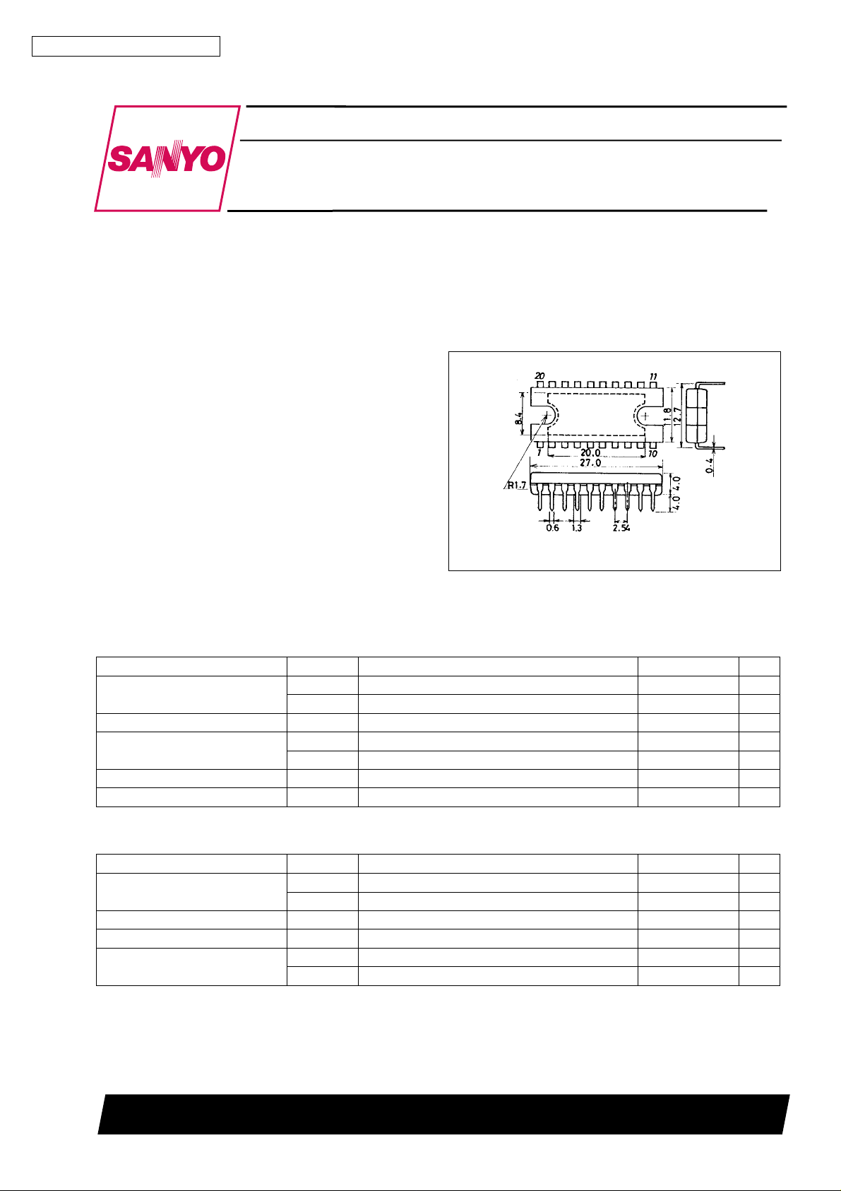
Package Dimensions
unit : mm
3037A-DIP20H
[LB1696]
Features
.
3-phase brushless motor driver.
.
Withstand voltage: 60 V; output current: 2.5 A.
.
Current limiter built in.
.
Low-voltage protector built in.
.
Thermal shutdown protector built in.
.
Hall amplifier with hysteresis built in.
.
FG output function.
.
Regulator built in.
SANYO : DIP20H
Specifications
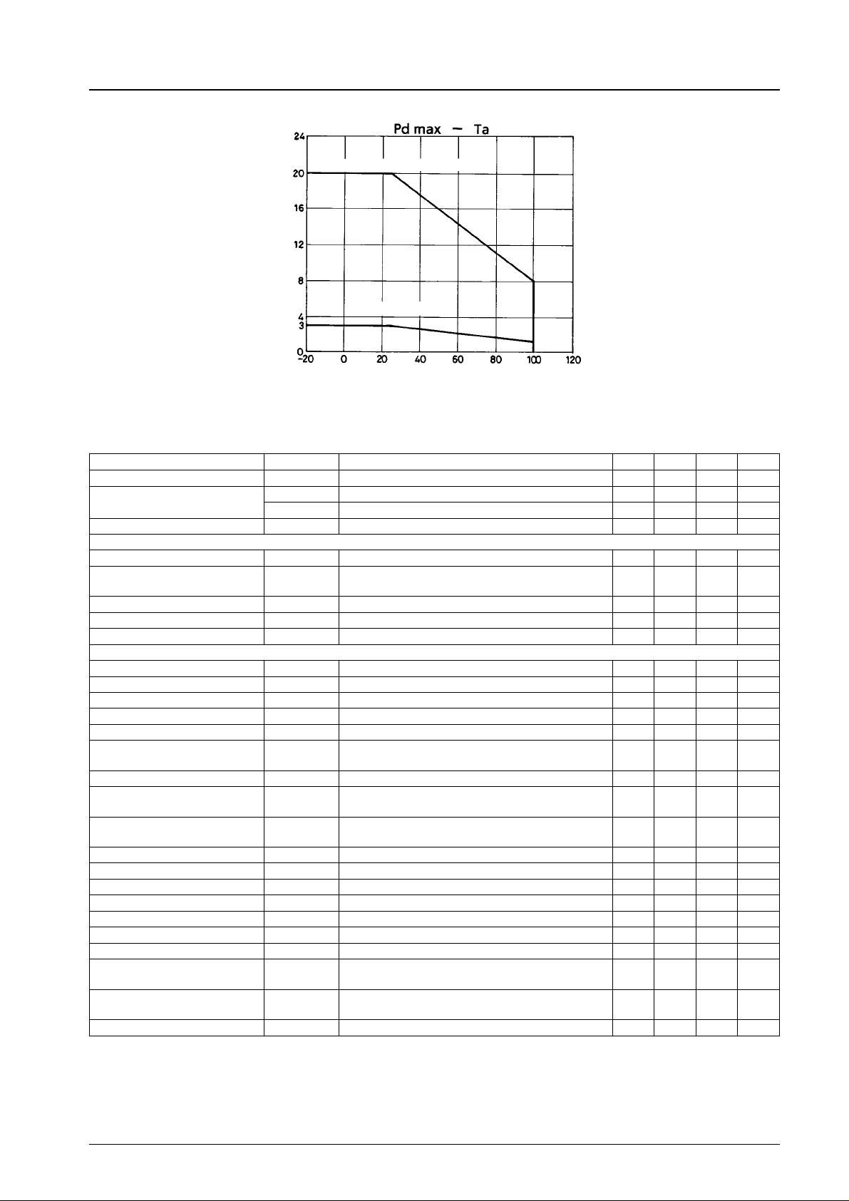
Absolute Maximum Ratings atTa=25°C
Parameter Symbol Conditions Ratings Unit
V
max 10 V
Maximum supply voltage
Output current I
Allowable power dissipation
Operating temperature Topr –20 to +100
Storage temperature Tstg –55 to +150
CC
V
max 60 V
M
O
Pd max1 Independent IC 3 W
Pd max2 With arbitrarily large heat sink 20 W
2.5 A
C
°
C
°
Allowable Operating Ranges atTa=25°C
Parameter Symbol Conditions Ratings Unit
V
Supply voltage range
Regulator input voltage V
V
pin output current I
REG
Power supply voltage rise rate
*1 If the supply voltage rise rate is fast when power is applied, through current may flow to output.
CC
V
M
(REG) 7 to 56 V
M
REGO
∆V
/ ∆tVCC=V
CC
∆V
/ ∆tVM= 0 V point*1 to 0.16 V/µs
M
(OFF) point*1 to 0.04 V/µs
LVSD
SANYO Electric Co.,Ltd. Semiconductor Bussiness Headquarters
TOKYO OFFICE Tokyo Bldg., 1-10, 1 Chome, Ueno, Taito-ku, TOKYO, 110 JAPAN
D3095HA(II) No.5244-1/9
4.5 to 6.0 V
5to56 V
400(max) µA
LB1696
With arbitrarily large heat sink
Independent IC
Allowable power dissipation, Pd max — W
Ambient temperature, Ta —°C
Electric Characteristics atTa=25°C, VCC=5V,VM=45V
Parameter Symbol Conditions min typ max Unit
Supply current I
Output saturation voltage
Output leakage current I
CC
V
Osat1IO
V
Osat2IO
O(leak)
Hall amplifier
Input bias current I
Common-mode input voltage
range
HB
V
ICM
Hysteresis width ∆V
Input voltage L → HV
Input voltage H → LV
SLH
SHL
FG pin (rate pulse output)
Output low level voltage V
Dull-up resistance R
Forward F/R operation V
Reverse F/R operation V
Current limit operator limiter V
Thermal shutdown operation
temperature
FGL
FR1
FR2
T
FG
RF
SD
Hysteresis width ∆T
Reduced voltage protection
operation voltage
Reduced voltage protection
release voltage
Hysteresis width ∆V
C pin charge current 1 I
C pin charge current 2 I
C pin discharge current I
C pin charge start voltage V
C pin discharge start voltage V
Output current neglect time t
Output off time 1 t
Output off time 2 t
Regulator output voltage V
V
LVSD
V
LVSD(OFF)
LVSD
CL
CL
CH
CL
CH
sm
so
so
CC(REG)
Forward 16 23 mA
= 1 A, VO(sink) + VO(source) 2.1 3.0 V
= 2 A, VO(sink) + VO(source) 3.0 4.2 V
IN
IFG= 5 mA 0.4 V
Design target 150 165
Design target 25
SD
1 R1=68kΩ, R2 = open 15 21 27 µA
2 R1=68kΩ,R2=10kΩ 111 158 205 µA
R1=68kΩ 168 225 282 µA
R1=68kΩ 0.3 0.4 0.5 V
R1=68kΩ 1.5 2.0 2.5 V
R1=68kΩ, C = 6800 pF 42 51 60 µs
R1=68kΩ, R2 = open,
1
C = 6800 pF
R1=68kΩ,R2=10kΩ,
2
C = 6800 pF
100 µA
14µA
1.5 3.2 V
27 32 36 mV
816 23mV
–23 –16 –8 mV
7.5 10 12.5 kΩ
0 0.8 V
4.2 5.0 V
0.42 0.5 0.6 V
3.5 3.8 4.1 V
4.3 4.5 V
0.4 0.5 0.6 V
462 545 628 µs
51 74 97 µs
4.5 5.2 5.9 V
C
°
C
°
No.5244-2/9
Truth Table
Input F/R control Output FG output
IN1 IN2 IN3 F/R Source → Sink FG1 FG2
1HLH
2HLL
3HHL
4LHL
5LHH
6LLH
LB1696
L OUT2 → OUT1
H OUT1 → OUT2
L OUT3 → OUT1
H OUT1 → OUT3
L OUT3 → OUT2
H OUT2 → OUT3
L OUT1 → OUT2
H OUT2 → OUT1
L OUT1 → OUT3
H OUT3 → OUT1
L OUT2 → OUT3
H OUT3 → OUT2
LL
LH
LL
HH
HL
HH
F/R
Forward L 0.0 to 0.8 V
Reverse H 4.2 to 5.0 V
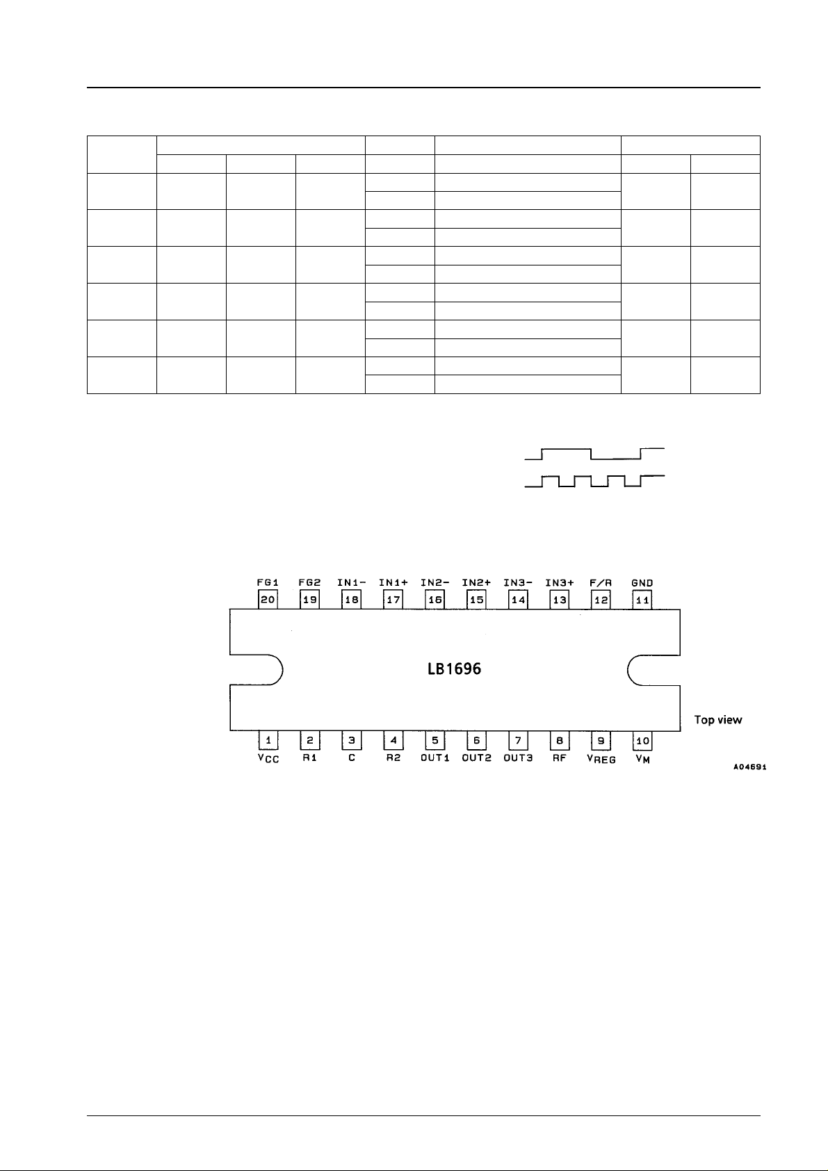
Pin Assignment
FG output
FG1
FG2
No.5244-3/9
 Loading...