

SANYO LB1695 Datasheet
Overview
The LB1695 is a three-phase brushless motor driver IC
that is optimal for DC fan motor drive in home appliances
such as on-demand water heaters.
Features
• Three-phase brushless motor drive
• 45-V voltage handling capacity, 2-A output current
• Current limiter circuit
• Low-voltage protection circuit
• Thermal shutdown protection circuit
• Hall amplifiers with hysteresis characteristics
• FG output function
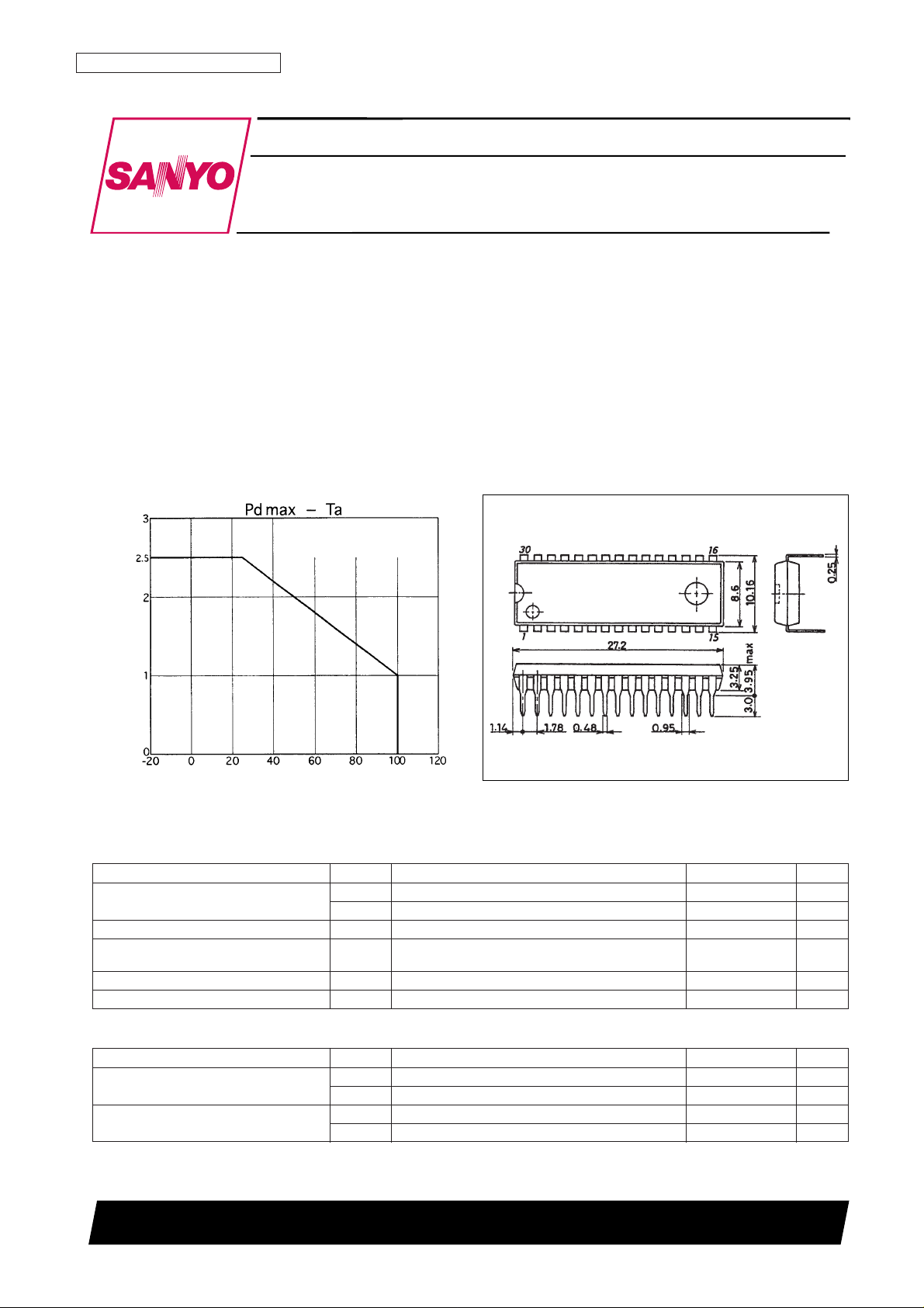
Package Dimensions
unit: mm
3196-DIP30SD
Monolithic Digital IC
Ordering number : EN5678
63097HA(OT) No. 5678-1/7
SANYO: DIP30SD
[LB1695]
SANYO Electric Co.,Ltd. Semiconductor Bussiness Headquarters
TOKYO OFFICE Tokyo Bldg., 1-10, 1 Chome, Ueno, Taito-ku, TOKYO, 110 JAPAN
Three-Phase Brushless Motor Driver
LB1695
Parameter Symbol Conditions Ratings Unit
Supply voltage
V
CC
10 V
V
M
45 V
Output current I
O
2.0 A
Allowable power dissipation Pd max
Mounted on a printed circuit board (114.3
× 76.2 × 1.6 mm
3
2.5 W
glass-epoxy board)
Operating temperature Topr –20 to +100 °C
Storage temperature Tstg –55 to +150 °C
Specifications
Absolute Maximum Ratings at Ta = 25°C
Parameter Symbol Conditions Ratings Unit
Power-supply voltage range
V
CC
4.5 to 5.5 V
V
M
5 to 42 V
Maximum power-supply slew rate at power on
∆V
CC
/∆t At VCC= V
LVSD
(OFF)* No more than 0.04 V/µs
∆V
M
/∆t At VM= 0 V* No more than 0.16 V/µs
Note: *These items are stipulated because output through currents can occur if the speed with which the power-supply voltage rises is too fast when power is
first applied.
Allowable Operating Ranges at Ta = 25°C
With a 20% wiring density on
a glass-epoxy board
114.3 × 76.2 × 1.6 mm
3
Ambient temperature, Ta – °C
Allowable power dissipation, Pdmax – W
No. 5678-2/7
LB1695
Parameter Symbol Conditions
Ratings
Unit
min typ max
Current drain I
CC
Forward rotation 13 19 mA
Output saturation voltage V
O
(sat)1 IO= 0.5 A, VO(sink) + VO(source) 1.8 2.4 V
V
O
(sat)2 IO= 1.0 A, VO(sink) + VO(source) 2.1 2.8 V
Output leakage current I
O
leak 100 µA
[Hall Amplifier]
Input bias current I
HB
1 4 µA
Common-mode input voltage range V
ICM
1.5 3.2 V
Hysteresis ∆V
IN
21 30 37 mV
Input voltage (low → high) V
SLH
5 15 25 mV
Input voltage (high → low) V
SHL
–25 –15 –5 mV
[FG Pin] (Speed pulse output)
Output low-level voltage V
FGLIFG
= 5 mA 0.4 V
Pull-up resistance R
FG
7.5 10.0 12.5 kΩ
[Forward/Reverse Operation]
Forward V
FR1
0 0.8 V
Reverse V
FR2
4.2 5.0 V
[Current Limiter Operation]
Limiter V
RF
0.42 0.5 0.6 V
[Thermal Shutdown Operation]
Operating temperature TSD * 150 180 °C
Hysteresis ∆TSD * 40 °C
[Low-Voltage Protection Operation]
Operating voltage V
LVSD
3.5 3.8 4.1 V
Release voltage V
LVSD(OFF)
4.3 4.5 V
Hysteresis ∆V
LVSD
0.4 0.5 0.6 V
[Pin C]
Charge current I
CL
R = 33 kΩ 30 40 50 µA
Discharge current I
CH
R = 33 kΩ 90 120 150 µA
Charge start voltage V
CL
R = 33 kΩ 0.3 0.4 0.5 V
Discharge start voltage V
CH
R = 33 kΩ 1.5 2.0 2.5 V
Output current ignored time t
sm
R = 33 kΩ, C = 4700 pF 58 68 78 µs
Output off time t
so
R = 33 kΩ, C = 4700 pF 164 193 222 µs
Electrical Characteristics at Ta = 25°C, VCC= 5 V, VM= 30 V
Note: *The items marked with an asterisk are design target values and are not tested.
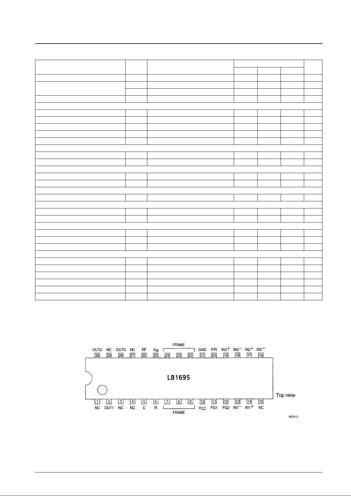
Pin Assignment
No. 5678-3/7
LB1695
Truth Table
F/R
Forward (low): 0.0 to 0.8 V
Reverse (high): 4.2 to 5.0 V
FG Output
Input Forward/reverse control Output FG output
IN1 IN2 IN3 F/R Source → sink FG1 FG2
1 H L H
L OUT2 → OUT1
L L
H OUT1 →OUT2
2 H L L
L OUT3 → OUT1
L H
H OUT1 →OUT3
3 H H L
L OUT3 → OUT2
L L
H OUT2 →OUT3
4 L H L
L OUT1 → OUT2
H H
H OUT2 →OUT1
5 L H H
L OUT1 → OUT3
H L
H OUT3 →OUT1
6 L L H
L OUT2 → OUT3
H H
H OUT3 →OUT2
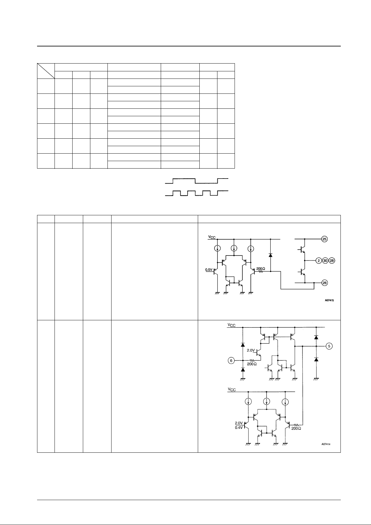
Pin Functions
Pin No. Pin Pin voltage(V) Pin function Equivalent circuit
2
30
28
25
26
OUT1
OUT2
OUT3
V
M
RF
• Output pin 1
• Output pin 2
• Output pin 3
• Power supply pin that provides the
output
• Output current detection
Connect the resistor Rf between this pin
and ground.
• The current limiter limits the output
current to the value set by V
RF
/Rf
(current limiter operation).
5
6
C
R
• The capacitor connected to this pin
determines both the time the output is
turned off when the current limiter
operates and the time the output current
is ignored.
• The resistor connected to this pin
determines the charge current for the pin
C capacitor.
Continued on next page.
FG1
FG2
 Loading...