SANYO LB1674V Datasheet

Ordering number: EN4392A
Monolithic Digital IC
LB1674V
Brushless, Sensorless Motor Driver
Overview
The LB1674V is a small motor driver ideal for mini-cassettes,
headphone stereos and micro-cassettes.
Functions and Features
c 3-phase unipolar, brushless, sensorless motor driver
c Reverse function
c Built-in speed control function (V servo)
c Built-in reference voltage (0.5 V)
c Soft switching driver
Specifications
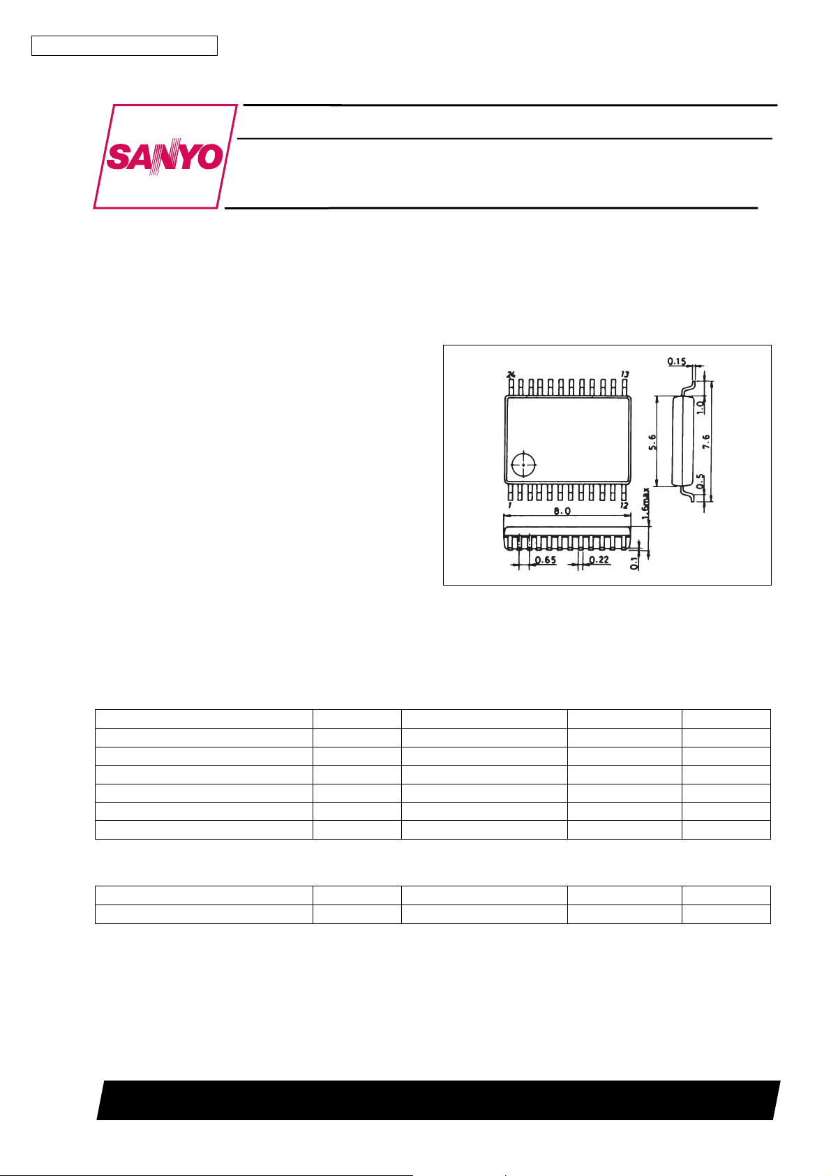
Package Dimensions
unit : mm
3175A-SSOP24
[LB1674V]
SANYO : SSOP24
Absolute Maximum Ratings at Ta = 25°C
Parameter Symbol Conditions Ratings Unit
Maximum supply voltage V
Output transistor withstand voltage Vsus 10 V
Maximum output current Im max 0.6 A
Allowable power dissipation Pd max Tj = 125°C 0.4 W
Operating temperature Topr 0 to + 80 °C
Storage temperature Tstg –40 to + 125 °C
max 5 V
CC
Allowable Operating Range at Ta = 25°C
Parameter Symbol Conditions Ratings Unit
Supply voltage V
CC
1.0 to 3.5 V
SANYO Electric Co.,Ltd. Semiconductor Bussiness Headquarters
TOKYO OFFICE Tokyo Bldg., 1-10, 1 Chome, Ueno, Taito-ku, TOKYO, 110 JAPAN
83096HA(II)/90793TS No.4392-1/6

LB1674V
Electrical Characteristics at Ta = 25°C, VCC= 1.5 V, unless otherwise noted
Parameter Symbol Conditions min typ max Unit
Supply current I
Reference voltage Vref 0.47 0.50 0.53 V
Reference-voltage characteristic
Reference-voltage load
characteristics
Reference-voltage temperature
characteristics
Speed signal detection accuracy Vsp V
Speed signal interphase error –5 +5 %
Speed-signal voltage
characteristics
Speed-signal temperature
characteristics
Current detection accuracy V
Current detection ratio K
Starting pulse period T
COM* lead-in current I
Output saturation voltage Vsat V
Logic input high-level voltage V
Logic input low-level voltage V
TC pin lead-in current I
∆Vref
Vref
∆Vref
Vref
∆Vsp
Vsp
∆Vsp
Vsp
CC
/ ∆V
∆Vref
∆Iref
/ ∆Ta
/ ∆V
/ ∆Ta
RI
COM
TC
START pin: high 6.5 10 mA
START pin: low 0 10 µA
CCVCC
CCVCC
I
S
* 25 35 45 µA
H
L
= 1.0 to 3.5 V 1 1.5 %/V
Iref=0to–50µA –0.2 –0.06 mV/µA
Ta=0to80°C 0.01 %/°C
= 750 mV 140 155 170 mV
IN
= 1.0 to 3.5 V 2 3 %/V
= 0.75 V, Ta=0to80°C 0.05 %/°C
V
IN
VIN1 = 0.3 V, VIN2 = 1.0 V, RI = 330 Ω 70 85 100 mV
VIN1 = 0.3 V, VIN2=1to1.3V 0.17 0.22 0.27
CS= 0.1 µF 32 ms
= 1.0 V, Im = 0.3 A 0.15 0.25 V
CC
0.9 V
0.3 V
35 50 65 µA
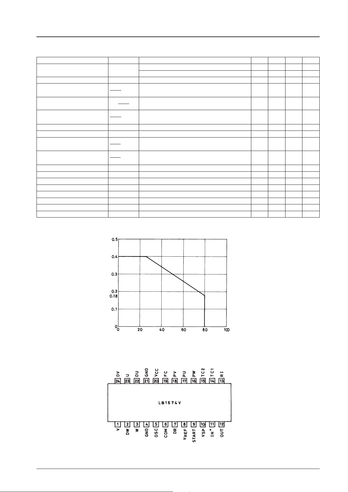
Pin Assignment
Pd max – Ta
Allowable power dissipation, Pd max – W
Ambient temperature, Ta – °C
Top view
No.4392-2/6
 Loading...