

SANYO LB1638M, LB1638 Datasheet
Ordering number: EN3515A
Monolithic Digital IC
LB1638, 1638M
Low-Saturation Bidirectional Motor Drive
for Low-Voltage Applications
Overview
The LB1638, 1638M are low-saturation bidirectional motor
driver ICs for use in low-voltage applications. At an I
500 mA, they have a low saturation output of V
0.75 V. They are especially suited for use in compact motor of
portable equipment.
O
O
(sat) =
of
Features
.
Low voltage operation (2.5 V min.)
.
Low saturation voltage (upper transistor + lower transistor
residual voltage; at I
.
Low current drain at standby mode (I
less)
.
Separate logic power supply and motor power supply
.
Brake function
.
Built-in spark killer diodes
.
Compact package (MFP-10S) suited for surface mounting.
= 500 mA, VO(sat) = 0.75 V typ.)
O
= 0.1 µA typ. or
CCO
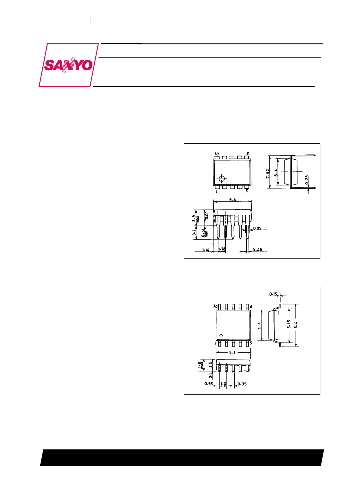
Package Dimensions
unit : mm
3098B-DIP10S
[LB1638]
SANYO : DIP10S
unit : mm
3086A-MFP10S
[LB1638M]
SANYO : MFP10S
SANYO Electric Co.,Ltd. Semiconductor Bussiness Headquarters
TOKYO OFFICE Tokyo Bldg., 1-10, 1 Chome, Ueno, Taito-ku, TOKYO, 110 JAPAN
73096HA(II)/7190TA(GTPS) No.3515-1/4

LB1638, 1638M
Specifications
Absolute Maximum Ratings atTa=25°C
Parameter Symbol Conditions Ratings Unit
V
max –0.3 to +10.5 V
Maximum supply voltage
Output applied voltage V
Input applied voltage V
Ground pin flow-out current I
Allowable power dissipation Pd max
Operating temperature Topr –20 to +75
Storage temperature Tstg –40 to +125
* Specified board (30 × 30 × 1.5 mm3glass epoxy)
Allowable Operating Ranges atTa=25°C
Parameter Symbol Conditions Ratings Unit
Supply voltage range
Input high-level voltage V
Input low-level voltage V
CC
V
max –0.3 to +10.5 V
S
OUT
GND
V
CC
V
IN
LB1638 1.0 W
LB1638M: Independent IC 440 mW
LB1638M: *With board 550 mW
S
IH
IL
–0.3 to VS+VF V
–0.3 to +10.0 V
2.5 to 9.0 V
2.2 to 9.0 V
2.0 to 9.0 V
–0.3 to +0.7 V
1.0 A
C
°
C
°
Electrical Characteristics atTa=25°C, VCC=VS=3V
Parameter Symbol
0VIN1, 2 ICC+I
I
CC
I
Current drain
Output saturation voltage
(upper + lower)
Output pin voltage difference I
Output sustain voltage V
Input current I
[Spark killer diode]
Reverse current I
Forward voltage V
1VIN1=3V,VIN2=0V ICC+I
CC
I
2VIN1,2=3V ICC+I
CC
V
1I
OUT
V
2I
OUT
(sus) I
O
IN
(leak) VCC,VS=7V 10 µA
S
SF
= 200 mA 0.25 0.5 V
OUT
= 500 mA 0.70 1.3 V
OUT
= 200 mA 0.1 V
O
= 500 mA 9 V
OUT
VIN=7V,VCC= 7 V 0.5 mA
I
= 200 mA 1.7 V
OUT
Conditions
Pin Assignment
min typ max Unit
S
S
S
10 µA
20 mA
40 mA
Top view
Note: both ground pins must be grounded.
No.3515-2/4
 Loading...