

SANYO LB1412 Datasheet
Ordering number: EN1218C
Monolithic Digital IC
LB1412
Level Meter Driver for 12 LEDs
Functions and Features
.
Bar-shaped display of input level by means of 12 LEDs
.
High-order 5 dots with peak hold
.
Built-in oscillator for peak hold reset. Requires 1 pce. each
of external C, R. Uses either oscillator at the time of stereo
operation. Capable of also resetting manually.
.
Capable of constant-current driving low-order 7 dots (green
LED). Constant-current value variable with an external
resistor
.
Lower current drain available by connecting green LEDs in
series
.
Built-in input amplifier
.
Requires no other light-up level adjustment than adjustment
for 0 dB. D1 error: within ±3dBof20dB
.
Supply voltage range : 10 to 16 V
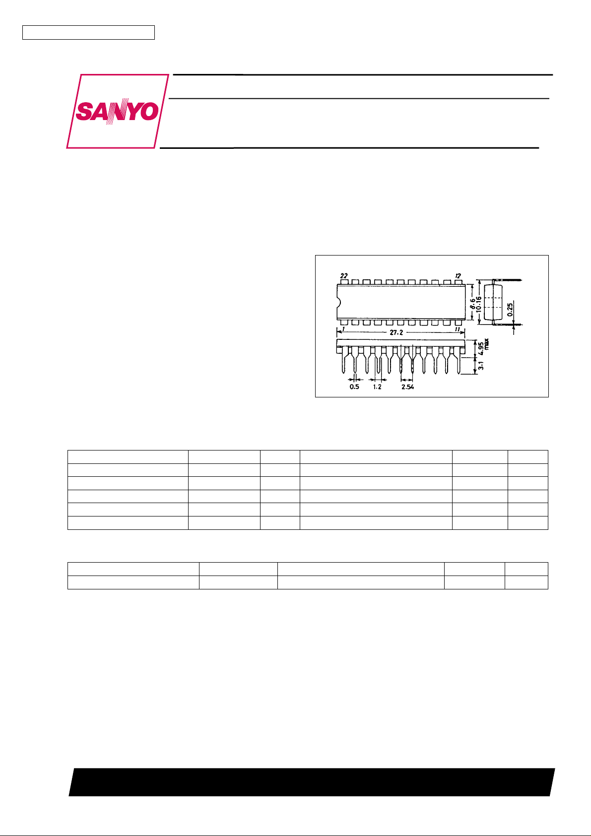
Package Dimensions
unit : mm
3010A-DIP22
[LB1412]
SANYO : DIP22
Specifications
Absolute Maximum Ratings at Ta = 25°C
Parameter Symbol Pin No. Conditions Ratings Unit
Maximum supply voltage V
Output current I
Allowable power dissipation Pd max Ta = 60°C 650 mW
Operating temperature Topr −30 to +75 °C
Storage temperature Tstg −40 to +125 °C
max 15 −0.3 to+18 V
CC
OL
1 to 5 D8 to D12, output on 30 mA
Allowable Operating Range at Ta = 25°C
Parameter Symbol Conditions Ratings Unit
Supply voltage V
CC
10 to 16 V
SANYO Electric Co.,Ltd. Semiconductor Bussiness Headquarters
TOKYO OFFICE Tokyo Bldg., 1-10, 1 Chome, Ueno, Taito-ku, TOKYO, 110 JAPAN
53096HA(II)/9097KI/8075MW/113KI(KOT) No.1218-1/5

LB1412
Electrical Characteristics at Ta = 25°C, VCC=12V
Parameter Symbols Pin No. Conditions min typ max Unit
Input bias current Amp (1) I
Output saturation
voltage
Amp (1) V
Amp (1) V
Voltage gain Amp (1) V
Input resistance Amp (2) R
Load resistance Amp (2) R
Output current Amp (2) I
Voltage gain Amp (2) V
Output current I
Output saturation voltage
Output leak current
D8 V
D1 G
D2 G
D3 G
D4 G
Comparator level
D5 G
D6 G
D7 G
D9 G
D10 G
D11 G
D12 G
Reference voltage V
R pin flow-out current I
R pin voltage V
Oscillation frequency f
Current drain I
BIN1
OH01
OL01
GA1
IN2
02
OL02
GA2
OL
V
sat
V
sat
l
off
l
off
THD8
D1
D2
D3
D4
D5
D6
D7
D9
D10
D11
D12
Z
OLR
R
OSC
CC
7 −3 −0.2 0 µA
8 Pins 8, 9 short 10.5 11.2 11.6 V
8 Pins 8, 9 short 1.0 1.5 2.0 V
9 8 12 16 kΩ
10 35 50 65 kΩ
10 3 6 12 mA
19,22 D1,D5:3kΩacross VZand I
17, 18,
19, 21,
D2 to D4, D6 to D7 : Output
Transistor on across V
22
1 to 5 D8 to D12 : I
19, 22 D1, D5 : output transistor off 0 30 µA
1 to 15 D8 to D12 : output transistor off 0 30 µA
D8 : Voltage to turn on D8 by
1
applying DC voltage across VZand
I
NZ
16 D8 light-up level:0dB −23 −20 −17 dB
17 D8 light-up level:0dB −17 −15 −13 dB
18 D8 light-up level:0dB −12 −10 −8 dB
19 D8 light-up level:0dB −8 −7 −6 dB
20 D8 light-up level:0dB −6 −5 −4 dB
21 D8 light-up level:0dB −4 −3 −2 dB
22 D8 light-up level:0dB −1.5 −1 −0.5 dB
2 D8 light-up level:0dB 0.5 1 1.5 dB
3 D8 light-up level:0dB 2 3 4 dB
4 D8 light-up level:0dB 4 5 6 dB
5 D8 light-up level:0dB 7 8 9 dB
12 3 kΩ across VZand I
11 VR= 0 V, OSC pin: open −0.6 −0.3 −0.1 mA
11 OSC pin: open 0.4 0.7 0.9 V
13 1 MΩ, 2.2 µF across VCCand V
3kΩacross V
15
outputs off
OLD1 to D5
and I
Z
30 100 dB
1.8 2.0 2.2 times
13 17 20 mA
1.0 1.3 V
Z
and I
LED
LED
= 30 mA 1.5 2.0 V
−0.625 −0.55 −0.465 V
LED
LED
Z
, all D
5.6 6.3 6.8 V
1.5 2 2.5 s
915mA
Allowable power dissipation, Pd max – mW
Pd max – Ta
Ambient temperature, Ta – °C
No.1218-2/5
 Loading...