

SANYO LA70001 Datasheet
Overview
The LA70001 and LA70001M ICs provide record and
playback amplifiers for VHS format VCRs. A system with
an adjustment-free Y/C record current can be achieved by
combining the LA70001/M with an LA71000M or
LA71500M video signal processing IC.
Features
• Direct connection of the head to the playback amplifier
input allows the number of external devices to be
reduced.
• A fixed-current drive technique that is strongly resistant
to load fluctuations is adopted in the record amplifier for
stable recording characteristics. The record amplifier
includes a built-in AGC circuit.
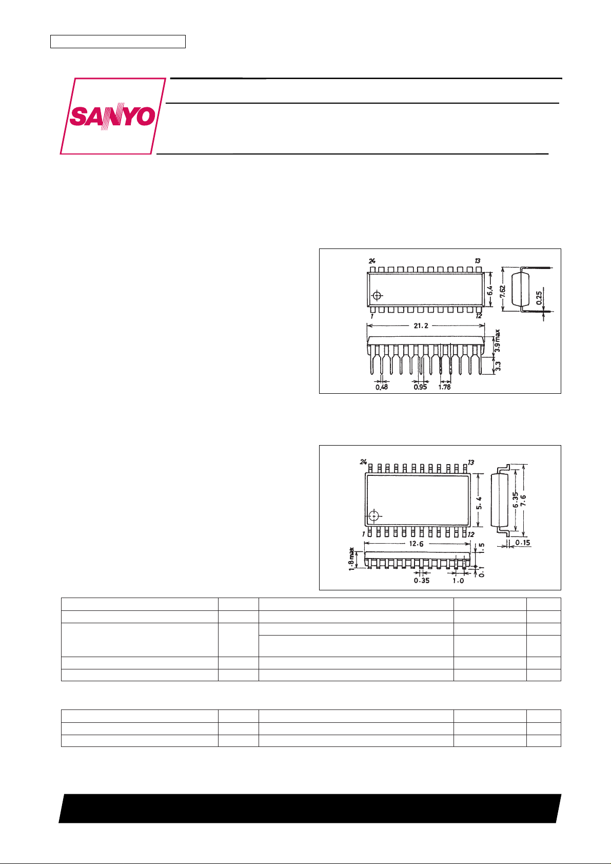
• These products have the same package dimensions as
the LA70011 and LA70011M to allow a common PCB
to be used. These products can also share the same PCB
with the LA70020 by mounting the IC at the right end of
the LA70020 socket.
Package Dimensions
unit: mm
3067-DIP24S
unit: mm
3112-MFP24S
Monolithic Linear IC
13098RM (OT) No. 5709-1/8
SANYO: DIP24S
[LA70001]
SANYO: MFP24S
[LA70001M]
SANYO Electric Co.,Ltd. Semiconductor Bussiness Headquarters
TOKYO OFFICE Tokyo Bldg., 1-10, 1 Chome, Ueno, Taito-ku, TOKYO, 110-0005 JAPAN
Record/Playback Amplifiers for VHS Format VCRs
LA70001, 70001M
Ordering number : EN5709
Parameter Symbol Conditions Ratings Unit
Maximum supply voltage V
CC
max 7.0 V
Ta ≤ 65°C [LA70001] 600 mW
Allowable power dissipation Pd max Ta ≤ 65°C [LA70001M]
500 mW
(Using a 114.3
× 76.1 × 1.6 mm glass epoxy PCB)
Operating temperature Topr –10 to +65 °C
Storage temperature Tstg –40 to +150 °C
Specifications
Maximum Ratings at Ta = 25°C
Parameter Symbol Conditions Ratings Unit
Recommended supply voltage V
CC
5.0 V
Operating supply voltage range V
CC
op 4.8 to 5.5 V
Operating Conditions at Ta = 25°C
No. 5709-2/8
LA70001, 70001M
Parameter Symbol Conditions
Ratings
Unit
min typ max
[Playback Mode]
Current drain I
CCP
The pin 13 inflow current. 23 29 35 mA
Voltage gain
CH1 G
VP
1 VIN= 38 m Vp-p, f = 1 MHz 56 59 62 dB
CH2 G
VP
2 56 59 62 dB
Voltage gain difference 1 ∆G
VP
1 GVP1—GVP2 –1 0 +1 dB
With the same conditions as for the voltage
Equivalent input noise voltage
CH1 V
NIN
1 gain, the ratio of the output passed through a
CH2 V
NIN
2 1.1-MHz low-pass filter and the output with no 1.0 1.5 µVrms
input signal.
Frequency characteristics CH1 ∆Vfp1 The ratio of the output for VIN= 38 mVp-p,
CH2 ∆V
fp
2 f = 7 MHz and GVP1, 2, 3, and 4. –2.5 0 dB
With V
IN
= 38 mVp-p, f = 4 MHz, the ratio of
Second harmonic distortion
CH1 V
HDP
1 the 8-MHz output component (second
CH2 V
HDP
2 harmonic) and the 4-MHz component (the –40 –35 dB
fundamental).
CH1 V
OMP
1
At f = 1 MHz, the output level when the ratio
Maximum output level
CH2 V
OMP
2
of the 3-MHz output (third harmonic) and the 1.0 1.2 Vp-p
1-MHz output (fundamental) is –30 dB.
Crosstalk SP V
CR
1
The ratio of the V
IN
= 38 mVp-p, f = 4 MHz
–40 –35 dB
output and G
VP
1.
Output DC offset ∆V
ODC
1 CH1 – CH2 –100 0 +100 mV
Envelope detector output pin voltage V
ENV
The T6 DC level when there is no input signal. 0 0.8 1.3 V
V
ENVSP
1
With a f = 4 MHz input, the T6 DC level when
2.0 2.5 3.0 V
Envelope detector output pin voltage SP1
the T7A output level becomes 175 mVp-p.
V
ENVSP
2
With a f = 4 MHz input, the T6 DC level when
3.5 4.0 4.5 V
the T7A output level becomes 400 mVp-p.
V
ENVEP
1
With a f = 4 MHz input, the T6 DC level when
2.0 2.5 3.0 V
Envelope detector output pin voltage EP
the T7A output level becomes 125 mVp-p.
V
ENVEP
2
With a f = 4 MHz input, the T6 DC level when
4.0 4.5 5.0 V
the T7A output level becomes 300 mVp-p.
Switch transistor on resistance in playback
R
PON
18
Measure the difference in the DC levels with
4 6 Ω
mode a 1-mA and a 2-mA inflow current.
SW30 threshold level
SW30-1 Lch → Hch *1 1.2 5.0 V
SW30-2 Hch → Lch 0.0 0.8 V
[Record Mode]
Current drain I
CCR
The pin 13 inflow current. 43 50 57 mA
Record AGC amplifier output level V
RSP
The output level when VIN= 400 mVp-p, f = 4 MHz.
105 112 119 mVp-p
∆V
AGC
1-SP
At f = 4 MHz, when VIN= 700 mVp-p: the
0.5 1.0 dB
Record AGC amplifier control output level /VRSP, EP
characteristics
∆V
AGC
2-SP
At f = 4 MHz, when VIN= 100 mVp-p: the
–1.0 –0.5 dB
output level /VRSP, EP
Record AGC amplifier frequency
At VIN= 400 mVp-p, the ratio of the outputs
characteristics
∆V
FRS
when f is 1 MHz and 7 MHz, i.e. the ratio of –1 0 +1 dB
the 7-MHz value to the 1-MHz value.*2.
With VIN= 400 mVp-p, f = 4 MHz, the ratio
Record AGC amplifier second harmonic
∆V
HDRS
of the 8-MHz output component (second
–45 –40 dB
distortion harmonic) and the 4-MHz component (the
fundamental).
Record AGC amplifier maximum output level ∆V
MOSP
At f = 4 MHz, the output level at which the
20 22 mAp-p
second harmonic goes to –35 dB. *3
Record AGC amplifier muting attenuation ∆V
MRS
When VIN= 400 mVp-p and f = 4 MHz, the
–45 –40 dB
output level/VRSP, EP
Record AGC amplifier cross modulation
T9A: VIN= 400 mVp-p, f = 4 MHz
relative level
∆V
CYS
T10A: VIN= 2.4 Vp-p, f = 629 kHz –45 –40 dB
The ratio of the (4 MHz ± 629 kHz) and the 4-MHz outputs.
Record muting threshold level
MUTE-1 MUTE OFF → MUTE ON *1 1.2 2.8 V
MUTE-2 MUTE ON → MUTE OFF 3.2 5.0 V
Record mode to playback mode threshold level
PB-REC PB →REC *1 1.2 5.0 V
REC-PB REC →PB 0.0 0.8 V
Electrical Characteristics at Ta = 25°C
Notes:Use a resistor with an accuracy of 1.0% for the resistor between pins 13 and 14.
*1. This is the voltage application point
*2. Here, fix the AGC amplifier gain by applying a 1.8-V DC level to the AGC detector filter pin (pin 15).
*3. Here, adjust the output level by applying a DC voltage to the REC-CUR-Adj pin (pin 12).
No. 5709-3/8
LA70001, 70001M
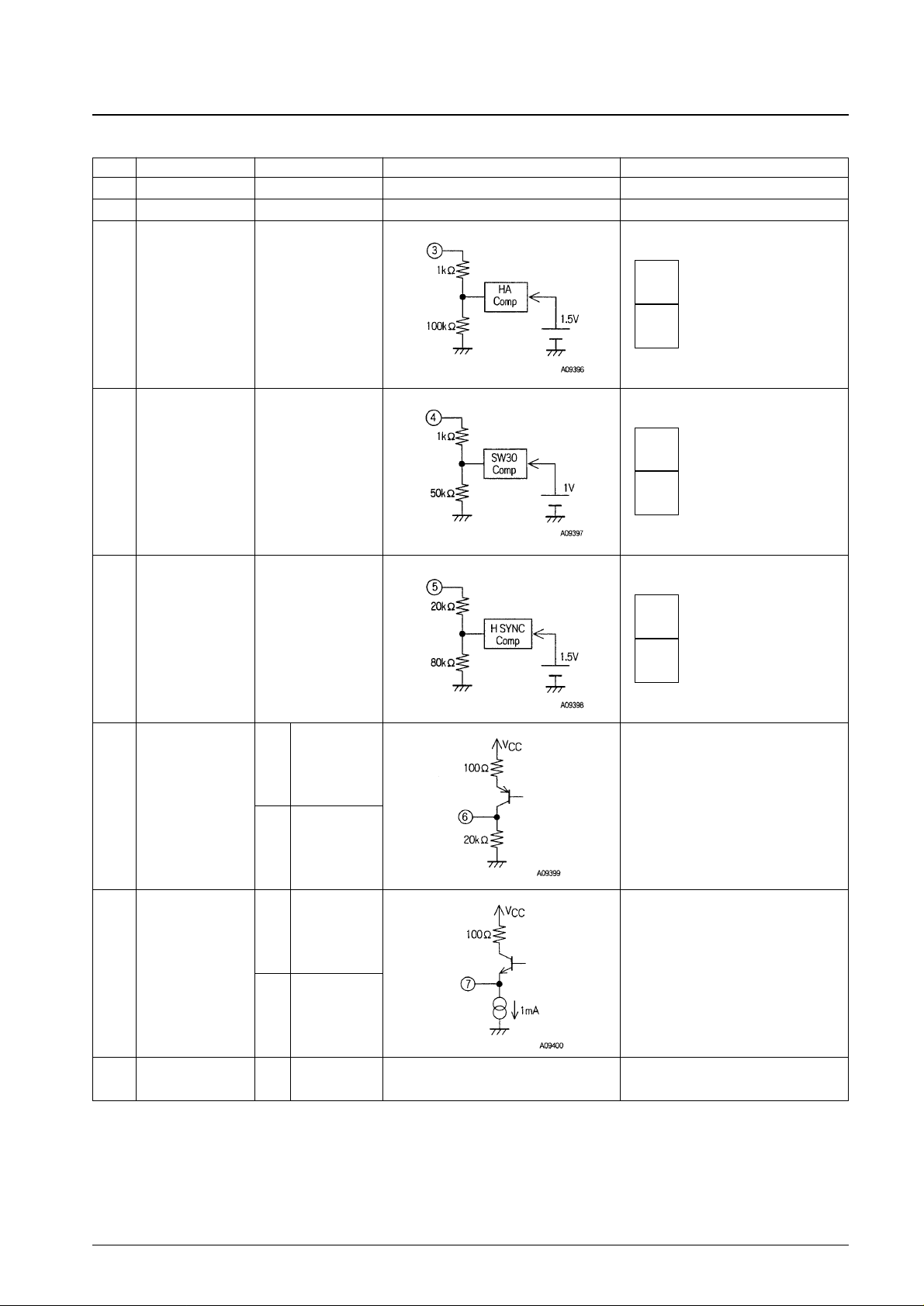
Pin Functions
Pin No. Pin name Standard DC voltage (V) Equivalent circuit Notes
1 N.C
2 N.C
3
4
5
6
7
8
20
HA (EP/SP)
SW30
H-SYNC
ENVDET-OUT
PB
REC
PB
REC
Provided in a
separate
document.
EP
1.5 V
SP
Hch
1.0 V
Lch
SYNC
H
1.5 V
L
0
1.7
2.1
PB-OUT
GND
Continued on next page.
 Loading...