

SANYO LA6602V Datasheet
Features
• The LA6602V is optimal as an interface IC between the
PD and servo ICs used in MD PU modules.
• Eight buffer amplifier channels
• On-chip low-noise high-bandwidth amplifier RF block
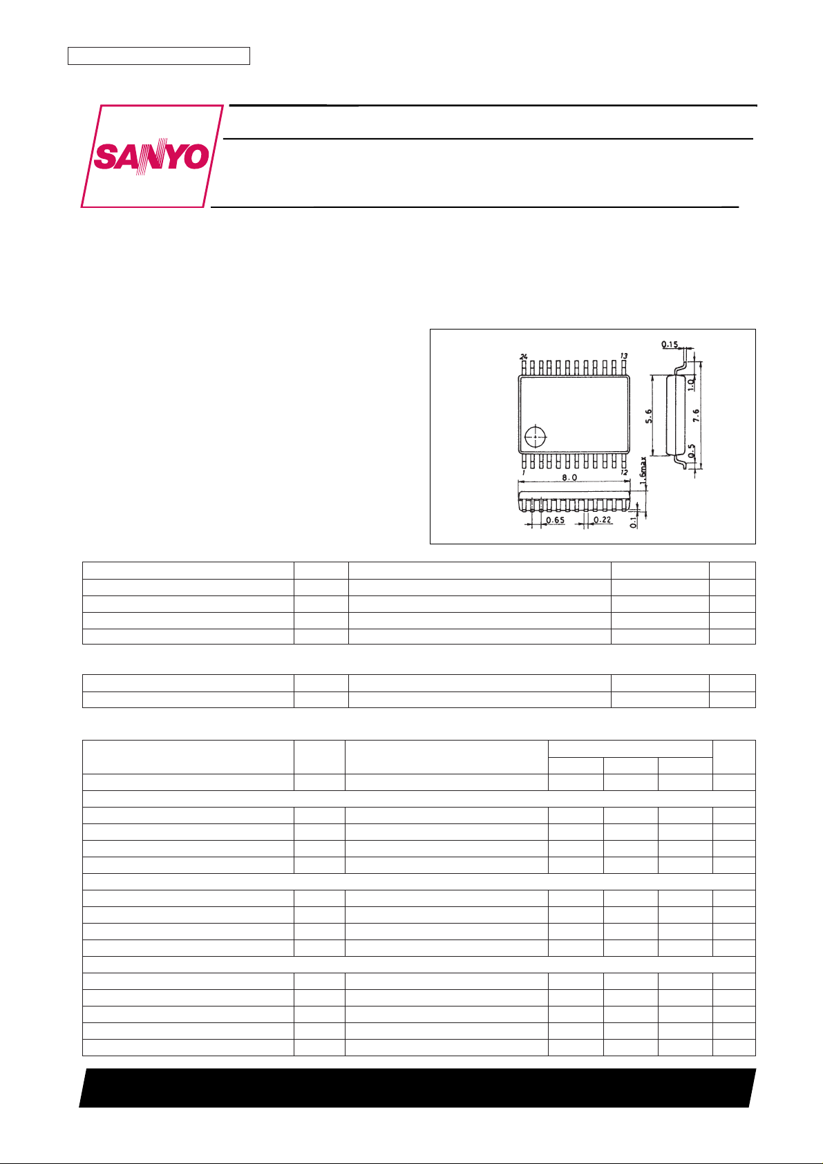
Package Dimension
unit: mm
3175A-SSOP24
Monolithic Linear IC
Ordering number : EN5307A
63097HA(OT) No. 5307-1/6
SANYO: SSOP24
[LA6602V]
SANYO Electric Co.,Ltd. Semiconductor Bussiness Headquarters
TOKYO OFFICE Tokyo Bldg., 1-10, 1 Chome, Ueno, Taito-ku, TOKYO, 110 JAPAN
I-V Amplifier for MiniDisc Drives
LA6602V
Parameter Symbol Conditions Ratings Unit
Maximum supply voltage V
CC
max 13.0 V
Allowable power dissipation Pd max Independent IC 300 mW
Operating temperature Topr –30 to +80 °C
Storage temperature Tstg –40 to +125 °C
Specifications
Maximum Ratings at Ta = 25°C
Parameter Symbol Conditions Ratings Unit
Supply voltage V
CC
3.6 to 12.0 V
Operating Conditions at Ta = 25°C
Parameter Symbol Conditions
Ratings
Unit
min typ max
Quiescent current I
CCO
See Figure 1. 5 10 20 mA
[Amplifiers A through D]
Output offset voltage V
IO
See Figure 2. 2 7 mV
Maximum output voltage V
O
max RL= 4.7 kΩ, VIN= –1 V See Figure 3. 2.0 V
Minimum output voltage V
O
min RL= 4.7 kΩ, VIN= +1 V See Figure 4. –2.0 V
Gain-bandwidth product f
T
20 [dB] amp GV = 0 [dB] See Figure 4. 0.5 0.7 MHz
[Amplifiers E and F]
Output offset voltage V
IO
See Figure 2. 2 7 mV
Maximum output voltage V
O
max RL= 4.7 kΩ, VIN= –1 V See Figure 3. 2.0 V
Minimum output voltage V
O
min RL= 4.7 kΩ, VIN= +1 V See Figure 4. –2.0 V
Gain-bandwidth product f
T
20 [dB] amp GV = 0 [dB] See Figure 4. 0.5 0.7 MHz
[Amplifiers I and J]
Output offset voltage V
IO
See Figure 2. 20 50 mV
Output offset voltage difference V
IO
I-J 3 7 mV
Maximum output voltage V
O
max RL= 2 kΩ, VIN= –1 V See Figure 3. 1.5 V
Minimum output voltage V
O
min RL= 2 kΩ, VIN= +1 V See Figure 4. –1.5 V
Gain-bandwidth product f
T
20 [dB] amp GV = 0 [dB] See Figure 4. 6 8 MHz
Operating Characteristics at Ta = 25°C, VCC/VEE= ± 2.5 V
No. 5307-2/6
LA6602V
Pin Functions
Pin No. Pin Function
1 I
OUT
IV amplifier I output
2 V
EE
IC substrate (lowest) voltage
3 E
OUT
IV amplifier E output
4 F
OUT
IV amplifier F output
5 F
IN
IV amplifier F input
6 E
IN
IV amplifier E input
7 I
IN
IV amplifier I input
8 J
IN
IV amplifier J input
9 NC Unused. Must be left open.
10 V
REF
External reference voltage
11 J
OUT
IV amplifier J output
12 NC Unused. Must be left open.
13 NC Unused. Must be left open.
14 D
OUT
IV amplifier D output
15 D
IN
IV amplifier D input
16 C
IN
IV amplifier C input
17 C
OUT
IV amplifier C output
18 B
OUT
IV amplifier B output
19 B
IN
IV amplifier B input
20 A
IN
IV amplifier A input
21 V
CC
Power-supply voltage
22 A
OUT
IV amplifier A output
23 NC Unused. Must be left open.
24 NC Unused. Must be left open.
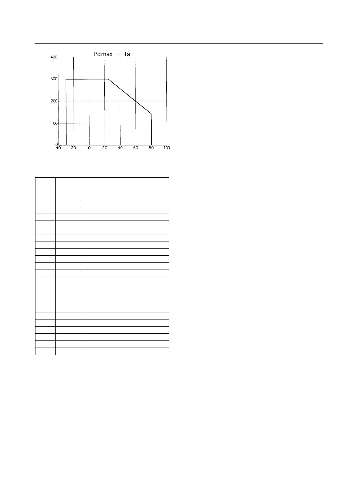
Ambient temperature, Ta – °C
Allowable power dissipation, Pd max – mW
 Loading...