

SANYO LA6557H Datasheet
Ordering number : ENN6350
51900RM (OT) No. 6350-1/8
Overview
The LA6557H is a five-channel bridge driver developed
for use in CD and MD players. It provides four BTL
power amplifier channels and one H-bridge power
amplifier channel.
Features and Functions
• Four BTL power amplifier channels and one H-bridge
power amplifier channel
•IOmax: 700 mA (each channel)
• Built-in level shifter circuits (BTL amplifiers)
• One muting circuit (output on/off control) system that
operates for the BTL amplifiers
• Thermal shutdown circuit built in
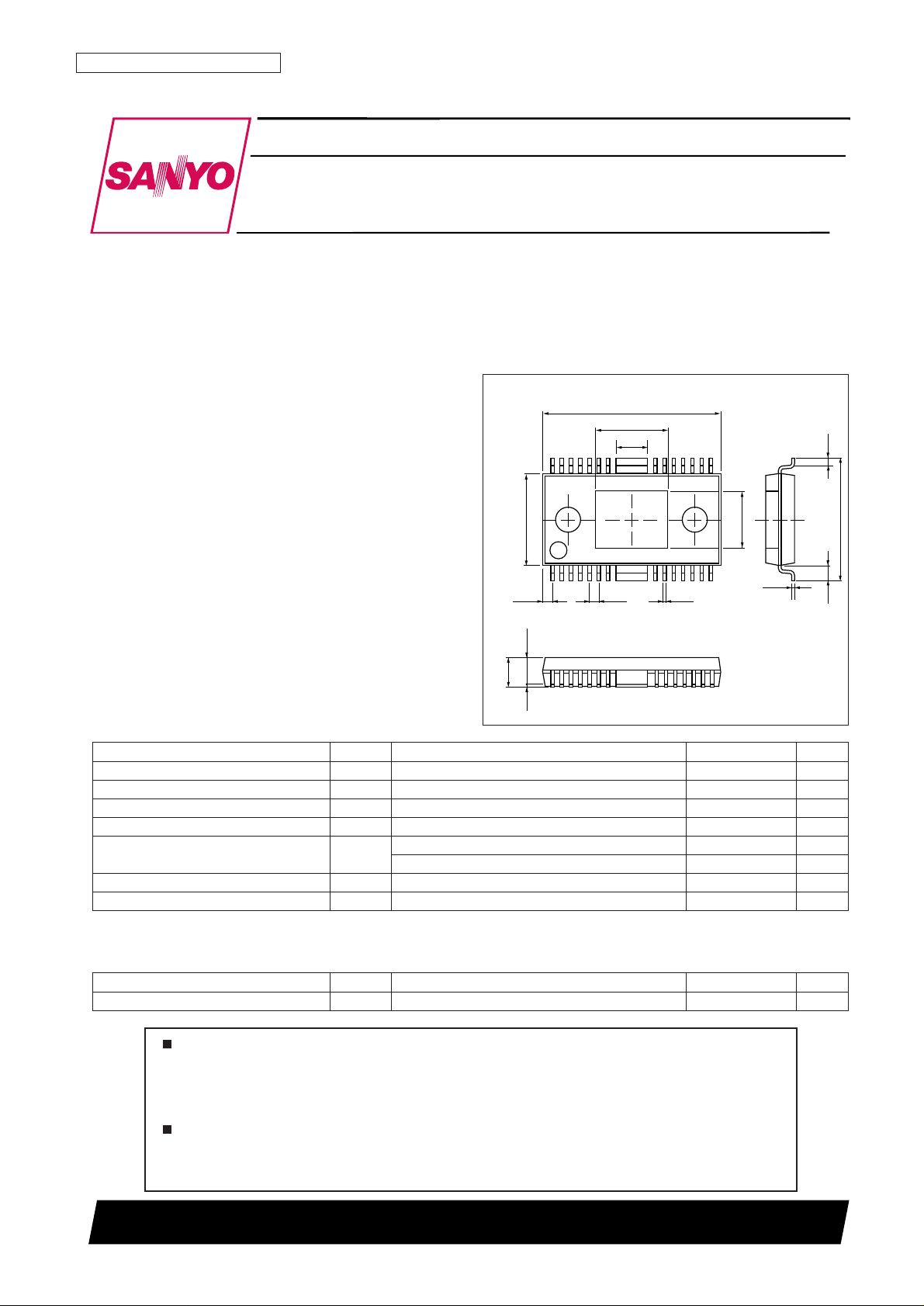
Package Dimensions
unit: mm
3234-HSOP28H-C
6.2
28 15
14
1
0.8
15.3
2.7
0.3
4.9
1.3
10.5
0.65
0.25
0.85
7.9
2.25
2.5max
0.1
SANYO: HSOP28H-C (375mil)
[LA6557H]
LA6557H
SANYO Electric Co.,Ltd. Semiconductor Company
TOKYO OFFICE Tokyo Bldg., 1-10, 1 Chome, Ueno, Taito-ku, TOKYO, 110-8534 JAPAN
Five-Channel Bridge Driver for MD and CD Players
Monolithic Linear IC
Any and all SANYO products described or contained herein do not have specifications that can handle
applications that require extremely high levels of reliability, such as life-support systems, aircraft’s
control systems, or other applications whose failure can be reasonably expected to result in serious
physical and/or material damage. Consult with your SANYO representative nearest you before using
any SANYO products described or contained herein in such applications.
SANYO assumes no responsibility for equipment failures that result from using products at values that
exceed, even momentarily, rated values (such as maximum ratings, operating condition ranges, or other
parameters) listed in products specifications of any and all SANYO products described or contained
herein.
Parameter Symbol Conditions Ratings Unit
Supply voltage V
CC
max 14 V
Maximum output current I
O
max For each channel in channels 1 to 5 0.7 A
Maximum input voltage V
IN
Bmax 13 V
Mute pin voltage V
MUTE
13 V
Allowable power dissipation Pd max
Independent IC 0.82 W
Mounted on the specified printed circuit board* 2.0 W
Operating temperature Topr –30 to +85 °C
Storage temperature Tstg –55 to +150 °C
Note: * Specified printed circuit board: 76.1 × 114.3 × 1.6 mm3glass-epoxy PCB
Specifications
Maximum Ratings at Ta = 25°C
Parameter Symbol Conditions Ratings Unit
Recommended supply voltage V
CC
5.6 to 13 V
Operating Conditions at Ta = 25°C
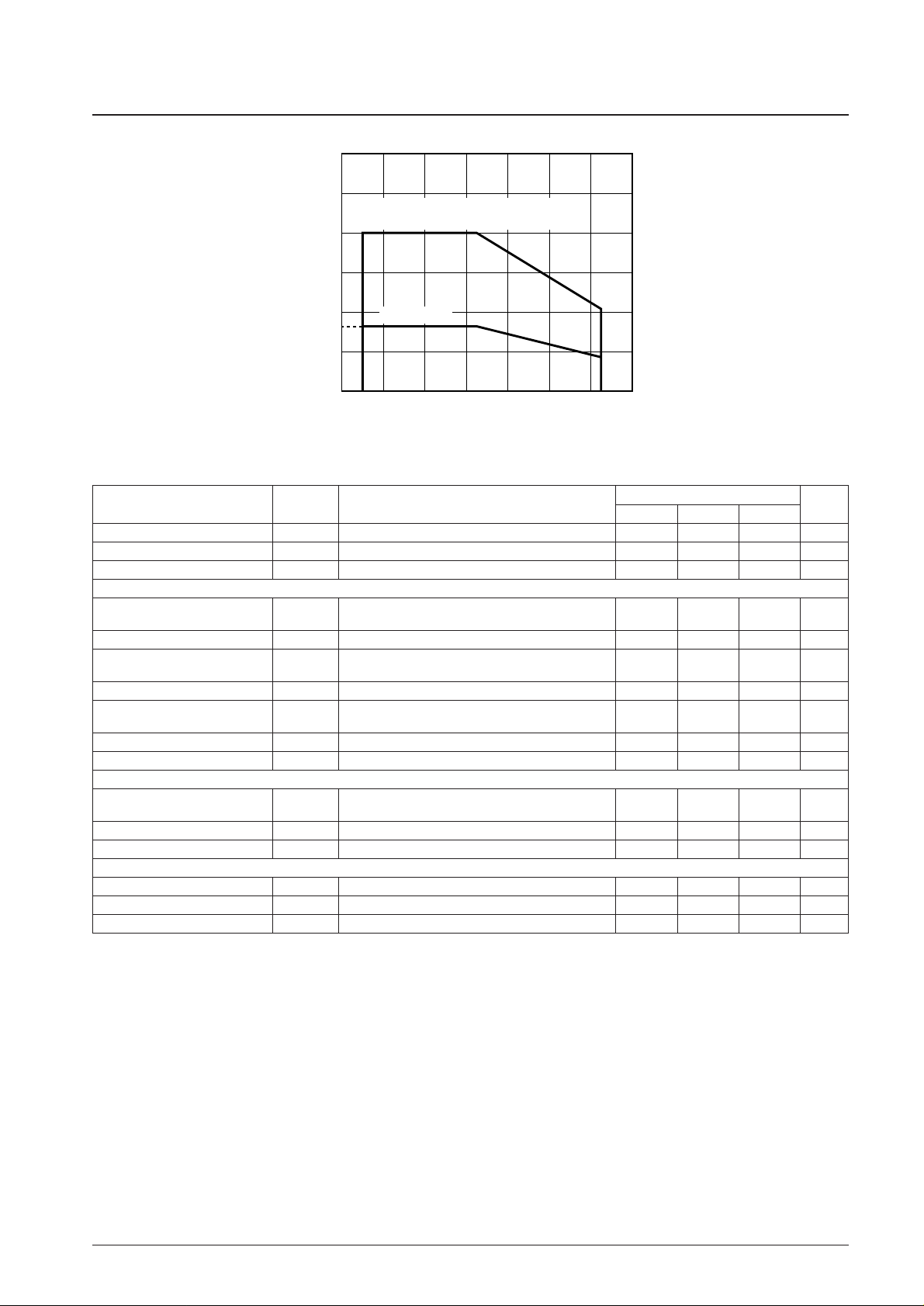
No. 6350-2/8
LA6557H
3.0
2.5
2.0
1.5
1.0
0.82
1.04
0.43
0.5
–
40–20
020406080100
0
Pd max — Ta
Allowable power dissipation, Pdmax — W
Independent IC
Ambient temperature, Ta — °C
–
30
Mounted on the specified printed circuit board
(76.1 × 114.3 × 1.6 mm
3
glass-epoxy board)
Parameter Symbol Conditions
Ratings
Unit
min typ max
No-load current drain: on I
CC
-ON All outputs on*1, FWD = REV = 0 V 30 50 mA
No-load current drain: off I
CC
-OFF All outputs off*1, FWD = REV = 0 V 10 20 mA
V
REF
input voltage range V
REF
-IN 1 VCC–1 V
[BTL Amplifier Block]
Output offset voltage V
OFF
The voltage difference between outputs for the
–50 +50 mV
BTL amplifiers
Input voltage range V
IN
The input voltage range 0 V
CC
V
Output voltage V
O
The voltage between VO+ and VO– for each channel
45 V
when R
L
= 8 Ω.*
2
Closed-circuit voltage gain V
G
Gain from input to output 12 dB
Slew rate SR
For independent amplifiers. Twice when measured
0.5 V/µs
between outputs *
4
Mute on voltage V
MUTE
-ON For each MUTE *
3
0.5 V
Mute off voltage V
MUTE
-OFF For each MUTE *
3
2V
[H Bridge Block]
Output voltage V
O
-LOAD
The voltage between V
O
+ and VO– for each channel
6V
when R
L
= 8 Ω.*
2
Low-level input voltage VIN-L 1V
High-level input voltage V
IN
-H 2 V
[Regulator Block]
Output voltage Vreg I
L
= 100 mA 4.75 5 5.25 V
Output load regulation ∆V
RLIL
= 0 to 200 mA –50 0 10 mV
Supply voltage regulation ∆VV
CCVCC
= 6 to 12 V, IL= 100 mA –15 21 60 mV
Electrical Characteristics at Ta = 25°C, VCC1 = VCC2 = 8 V, V
REF
= 1.65 V
Notes:1. The total current drain for VCC1 and VCC2 with no load.
2. The voltage across an 8 Ω load. With the output saturated.
3. MUTE: When the MUTE pin is high, the outputs will be on, and when low, off (high impedance)
4. These values are design guarantee values, and are not tested.
No. 6350-3/8
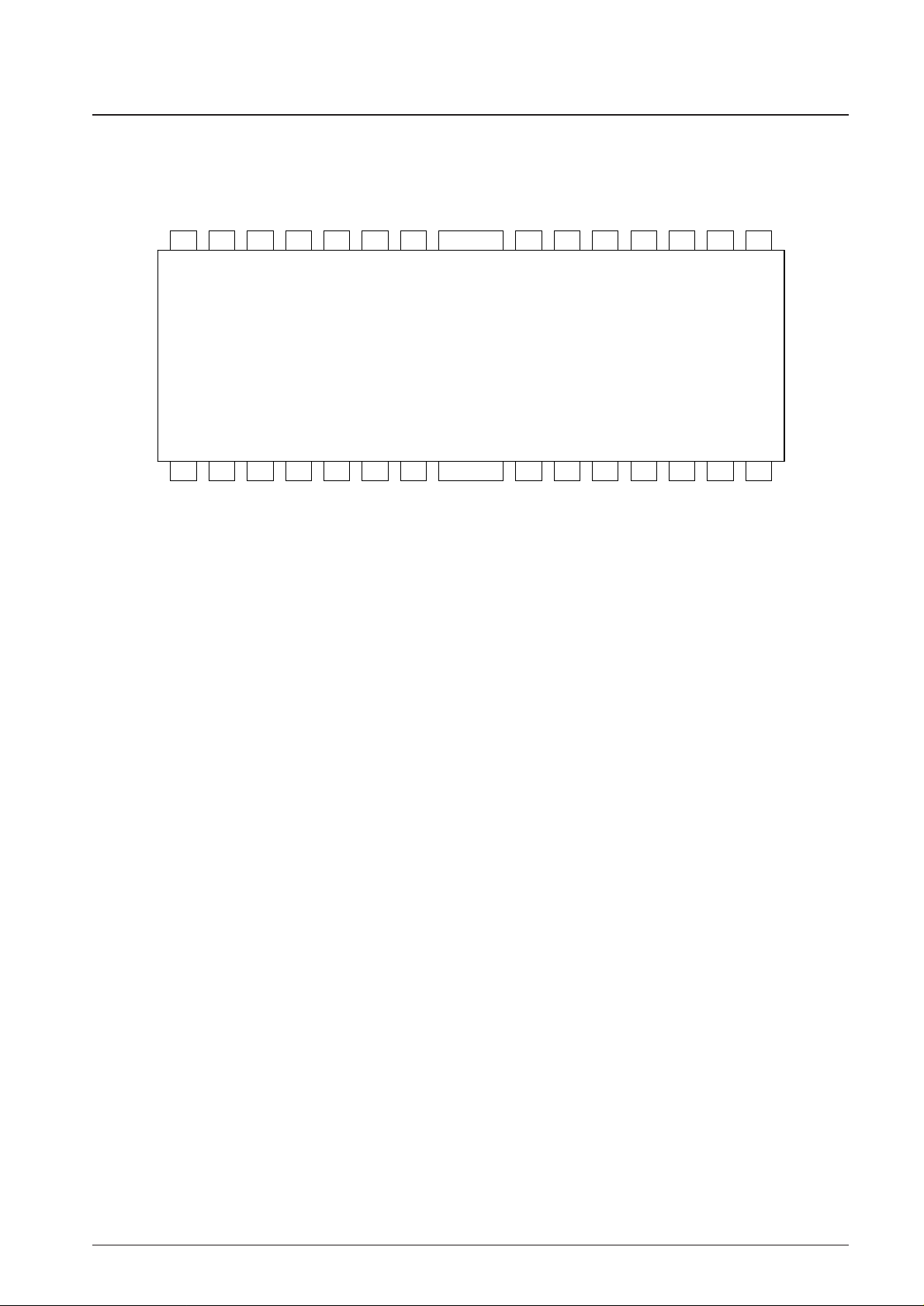
LA6557H
Pin Assignment
MUTE
1 2 3 4 5
1516
10 11 12 13 14
FR
27 26 22 21 20 19
FR
V
CC
1
V
O
1–
V
O
1+
V
O
2+
V
O
2–
V
O
4–
FWD
REV
V
O
5–
V
O
5+
V
O
3+
V
O
4+
V
IN
3
REG-IN
V
CC
-S
6 7 8 9
171823242528
V
IN
4G
V
IN
4
V
IN
2G
V
IN
3G
V
O
3–
V
CC
2
REG-OUT
V
REF
-IN
S-GND
V
IN
2V
IN
1G
V
IN
1
LA6557H
Top view
 Loading...