

SANYO LA6544M Datasheet
Ordering number : ENN6295
42800RM (OT) No. 6295-1/7
Overview
The LA6544M is a 4-channel bridge (BTL) driver
developed for use in CD-ROM systems.
Functions
• Bridge connected (BTL) four-channel power amplifier
•VCE(residual voltage) minimized (channels 1 to 3) by
using two power supplies.
•IOmax: 1.0 A
• Muting circuit provided (output on/off control)
(MUTE pin: low for output off, high for output on.
MUTE1: controls channel 1, MUTE2: controls channels
2, 3, and 4.)
• Thermal protection (shutdown) circuit
• Separated output stage power supply (VS1: channels 1,
2, and 3, VS2: channel 4)
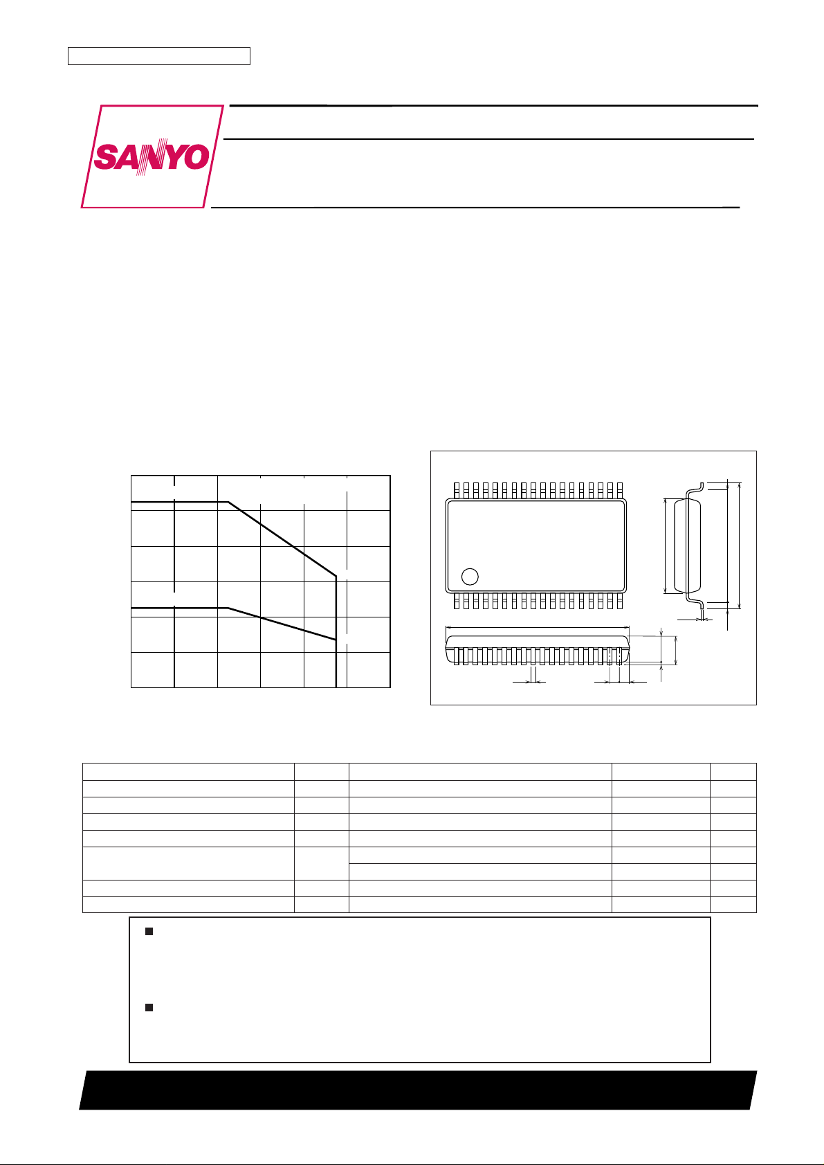
Package Dimensions
unit: mm
3129-MFP36SLF
0.25
15.3
118
36
19
0.85
0.4
0.8
2.5max
2.250.1
7.9
9.2
10.5
0.65
SANYO: MFP36SLF
[LA6544M]
LA6544M
SANYO Electric Co.,Ltd. Semiconductor Company
TOKYO OFFICE Tokyo Bldg., 1-10, 1 Chome, Ueno, Taito-ku, TOKYO, 110-8534 JAPAN
Four-Channel Bridge (BTL) Driver for CD-ROM
Monolithic Linear IC
Any and all SANYO products described or contained herein do not have specifications that can handle
applications that require extremely high levels of reliability, such as life-support systems, aircraft’s
control systems, or other applications whose failure can be reasonably expected to result in serious
physical and/or material damage. Consult with your SANYO representative nearest you before using
any SANYO products described or contained herein in such applications.
SANYO assumes no responsibility for equipment failures that result from using products at values that
exceed, even momentarily, rated values (such as maximum ratings, operating condition ranges, or other
parameters) listed in products specifications of any and all SANYO products described or contained
herein.
0.4
0.8
1.2
0.9
2.1
1.6
2.0
2.4
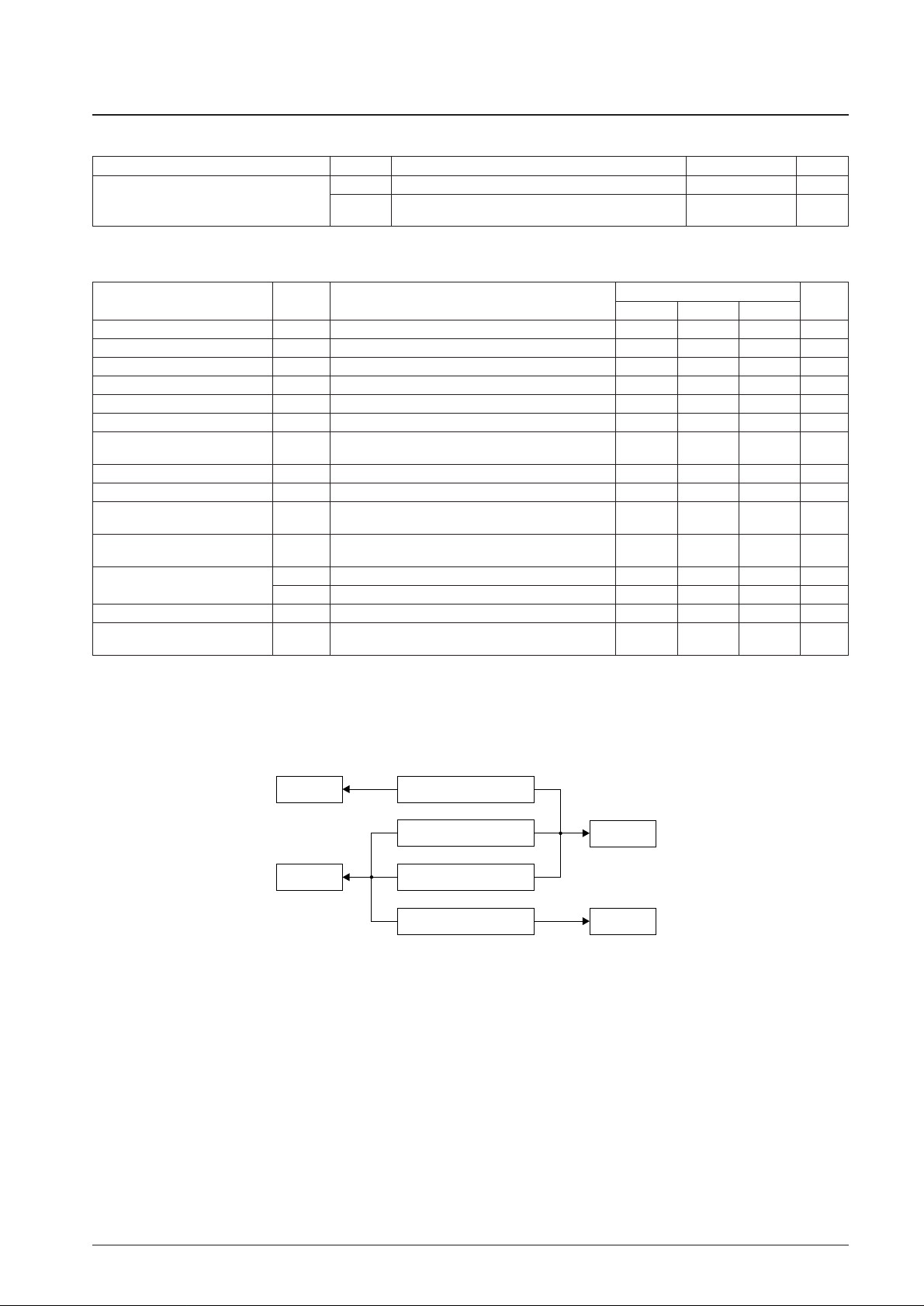
0
–20 0 20 40 60 75 80 100
Allowable power dissipation, Pdmax — W
Pd max — Ta
Ambient temperature, Ta — °C
PCB: 76.1 × 114.3 × 1.6 mm3,
glass epoxy
1.26
0.54
Mounted on a PCB
Independent IC
Parameter Symbol Conditions Ratings Unit
Maximum supply voltage 1 V
CC
max VCC≥ VS1, 2 14 V
Maximum supply voltage 2 V
S
max VS1, 2, VCC≥ VS1, 2 14 V
Input voltage V
IN
max Each of the input pins VIN1 to VIN413V
MUTE pin voltage V
MUTE
max 13 V
Allowable power dissipation Pd max
Independent IC 0.9 W
Mounted on the specified PCB (76.1 × 114.3 × 1.6 mm3, glass epoxy) 2.1 W
Operating temperature Topr –20 to +75 °C
Storage temperature Tstg –55 to +150 °C
Specifications
Maximum Ratings at Ta = 25°C
No. 6295-2/7
LA6544M
Parameter Symbol Conditions Ratings Unit
Operating supply voltage
V
CC
VCC≥ VS1, 2 4 to 13 V
V
S
1, 2
V
S
1 and VS2 are the output stage power supply.
4 to 13 V
V
CC
≥ VS1 and VS2
Recommended Operating Conditions at Ta = 25°C
Parameter Symbol Conditions
Ratings
Unit
min typ max
V
CC
no load current drain 1 ICC-ON Output on (MUTE1 and MUTE2: high), V
CC
10 25 mA
V
CC
no load current drain 2 ICC-OFF Output off (MUTE1 and MUTE2: low), V
CC
4mA
VS1 no load current drain 1 I
S
1-ON Output on (MUTE1 and MUTE2: high), VS12035mA
VS1 no load current drain 2 I
S
2-OFF Output off (MUTE1 and MUTE2: low), VS14mA
VS2 no load current drain 1 I
S
2-ON Output on (MUTE1 and MUTE2: high), VS2510mA
VS2 no load current drain 2 I
S
2-OFF Output off (MUTE1 and MUTE2: low), VS24mA
Output offset voltage V
OF
1 to 4
Potential difference between the + and – outputs for each
–50 +50 mV
channel
Input voltage range 1 V
IN
1 Input voltage range for channels 1, 2, and 3 0 VS1V
Input voltage range 2 V
IN
2 Input voltage range for channel 4 0 VS2V
Output voltage 1 VO1
I
O
= 700 mA, the difference between the outputs for
4 4.5 V
channels 1, 2, and 3
Output voltage 2 VO2
IO= 700 mA, the difference between the outputs for
10.5 11 V
channel 4
Closed circuit voltage gain
VG1 The BTL amplifier voltage gain for channels 1, 2, and 3 7 dB
VG2 The BTL amplifier voltage gain for channel 4 14 dB
Slew rate SR *
1
0.5 V/µs
Muting on voltage V
MUTE
MUTE1 and MUTE2. The voltage at which the output
1.5 2 V
turns on. *
2
Electrical Characteristics at Ta = 25°C, VCC= VS2 = 12 V, VS1 = 5 V, V
REF
= 2.5 V
Notes: 1. Design guarantee value.
2. The MUTE1, and MUTE2 pins turn the output on when high and off when low. When the output is off, the outputs will be in the high-impedance
state.
The figure below shows the relationship between the channels and the MUTE pins and between the channels and the power supplies.
System Figure
MUTE1 CH1 (7 dB)
CH2 (7 dB)
MUTE2 CH3 (7 dB)
CH4 (14 dB)
VS1
VS2
A12681
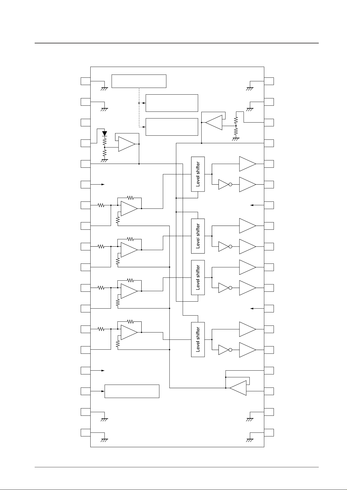
Block Diagram and Pin Assignment
No. 6295-3/7
LA6544M
1
2
3
4
5
6
7
8
9
10
11
12
13
14
15
16
17
18
RF
RF
(NC)
VSS2
VSS2-OUT
MUTE1 MUTE1
11 kΩ
12.5 kΩ
VIN1
VG1
VIN2
VG2
VIN3
VG3
VIN4
VG4
MUTE2
V
CC
RF
RF
36
35
34
33
32
31
30
29
28
27
26
25
24
23
22
21
20
19
RF
RF
VSS1
VSS1-OUT
VO1
+
VO1
–
VS1
VO2
+
VO2
–
VO3
+
VO3
–
VS2
VO4
+
VO4
–
V
REF
OUT
V
REF
IN
RF
RF
MUTE2
–
+
–
+
–
+
–
+
11 kΩ
12.5 kΩ
–
+
11 kΩ
12.5 kΩ
–
+
11 kΩ
27.5 kΩ
–
+
Input stage power supply
(all channels)
VS1 power supply
(channels 1, 2, and 3)
VS1 power supply (channel 4)
Thermal shutdown circuit
MUTE1
Channel 1 output on/off
MUTE2
Channels 2, 3, and 4 output on/off
A12682
 Loading...