

Sanyo LA6543 Specifications
Ordering number : EN5973
SANYO Electric Co., Ltd. Semiconductor Business Headquarters
TOKYO OFFICE Tokyo Bldg., 1-10, 1 Chome, Ueno, Taito-ku, TOKYO, 110-8534 JAPAN
LA6543
Monolithic Linear IC
LA6543
4-Channel Bridge (BTL) Driver for CD-ROM
Overview
The LA6543 is a 4-channel bridge (BTL) driver
developed for CD-ROM applications.
Features and Functions
• Integrated 4-channel power amplifier with bridge
circuit (BTL) (two output stage power supply lines)
• IOmax: 1A
• Integrated level shift circuit
• Integrated muting circuit
MUTE: Output OFF at Low, output ON at High.
MUTE1 is for channels 1 and 2, and MUTE2 for
channels 3 and 4.
• Integrated thermal shutdown circuit
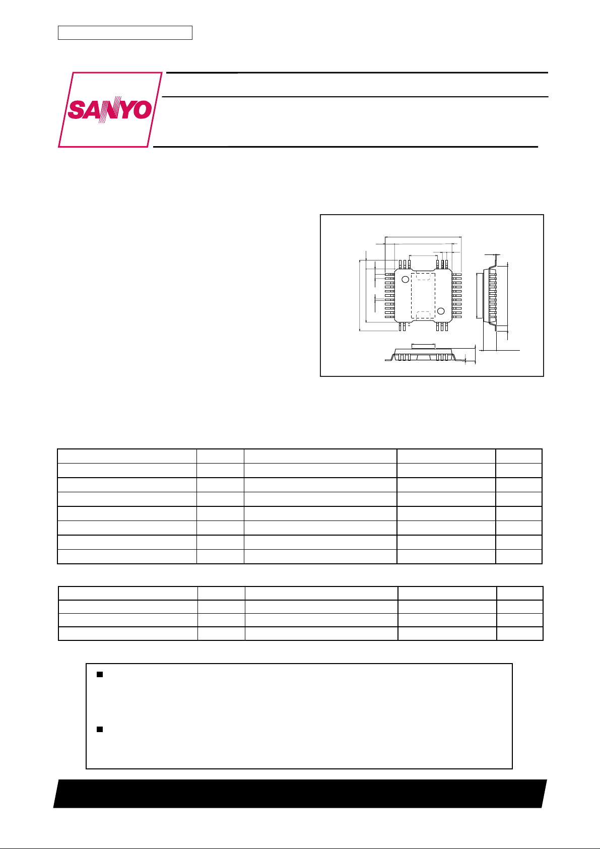
Package Dimensions
unit: mm
3219-QFP34HC
[LA6543]
13.2
10.0
4.8
16
4.0
13.2
1.6
10.0
1.6
1.0
0.8
0.35
24
34
1.0
0.8
1823
0.2
17
8.4
7
2.2
0.1
SANYO : QFP34HC
11.6
0.8
2.45max
• Divided output stage power supply (VS1: CH1, CH2,
CH3; VS2: CH4)
Specifications
Maximum Ratings at Ta = 25°C
Parameter Symbol Conditions Ratings Unit
Maximum supply voltage 1 14 V
Maximum supply voltage 2 14 V
Maximum input voltage 13 V
Mute pin voltage 13 V
Allowable power dissipation Pd max IC only 0.77 W
Operating temperature Topr °C
Storage temperature Tstg °C
VCCmax
VSmax
VINmax
V
MUTE
VS1, 2
Input pins VIN1 to 4
max
–20 to +75
–55 to +150
Operating Conditions at Ta = 25°C
Parameter Symbol Conditions Ratings Unit
Recommended operation voltage 1 4 to 13 V
Recommended operation voltage 2-1 4 to 13 V
Recommended operation voltage 2-2 4 to 13 V
* V
≥ VS1, 2
CC
Any and all SANYO products described or contained herein do not have specifications that can handle
applications that require extremely high levels of reliability, such as life-support systems, aircraft's
control systems, or other applications whose failure can be reasonably expected to result in serious
physical and/or material damage. Consult with your SANYO representative nearest you before using
any SANYO products described or contained herein in such applications.
SANYO assumes no responsibility for equipment failures that result from using products at values that
exceed, even momentarily, rated values (such as maximum ratings, operating condition ranges, or other
parameters) listed in products specifications of any and all SANYO products described or contained
herein.
V
VS1
VS2
CC
VS1: CH1 to CH3
VS2: CH4
output reference power supply
N1798RM(KI)
No. 5973-1/7
LA6543
Electrical Characteristics at V
Parameter
VCC no-load current drain
VS1 no-load current drain
V
2 no-load current drain
S
Output offset voltage
Input voltage range Input voltage range for 0.5 5 V
Output voltage (source) Plus and minus outputs at high level 4.4 4.7 V
(si n k ) Plus and minus outputs at low level 0.3 0.6 V
Closed circuit voltage gain1 VG1 Voltage gain between CH1 to CH3 BTL amplifiers 7 dB
Closed circuit voltage gain2 VG2 Voltage gain between CH4 BTL amplifiers 14 dB
Slew rate SR (Note 1) 0.5 V/µs
Mute ON voltage MUTE1, MUTE2 voltage when output is ON (Note 2) 1.5 2 V
Mute ON current MUTE1, MUTE2 voltage when output is ON (Note 2) 6 10 µA
= 12V, VS1 = 5V, VS2 = 12V, Ta = 25˚C
CC
Symbol
ICC1
ICC2
IS1-1
IS1-2
2-1
I
S
IS2-2
V
1 to4
OFF
V
IN
VOsource
V
sink
O
V
MUTE
I
MUTE
All outputs ON (MUTE1, MUTE2: High) 5 10 20 mA
All outputs OFF (MUTE1, MUTE2: Low) 5 10 mA
CH1 ON (MUTE1, MUTE2: High) 20 40 mA
CH1 OFF (MUTE1, MUTE2: Low) 4 mA
CH2 to CH4 ON (MUTE1, MUTE2: High) 5 10 mA
CH2 to CH4 OFF (MUTE1, MUTE2: Low) 4 mA
Potential difference between plus and minus outputs
for CH1 to CH4
I
= 700 mA
O
I
= 700 mA
O
Conditions
1 to VIN4
V
IN
Ratings
min typ max
–50 50 mV
Unit
Note 1: Guaranteed design value
Note 2: MUTE turns amplifier output ON at High and OFF at Low. (At Low, output impedance becomes high.) MUTE1 and MUTE2
operate independently on the respective channels.
1.0
0.8
0.6
0.4
0.2
IC Only
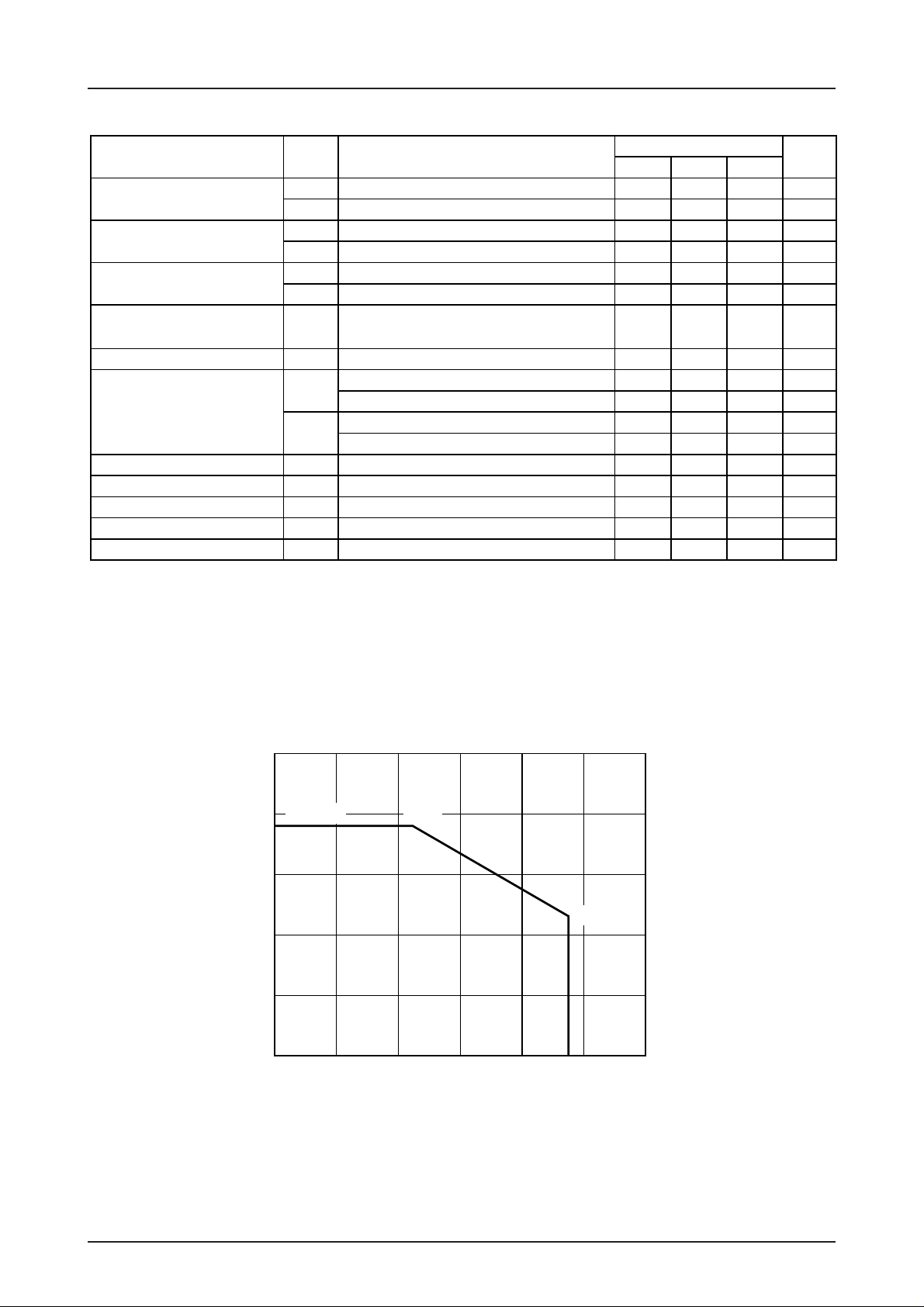
Pd max – Ta
0.77
0.46
Allowable power dissipation, Pd max – W
0
–20 0 20 40 60 80 100
Ambient temperature, Ta – ˚C
No. 5973-2/7
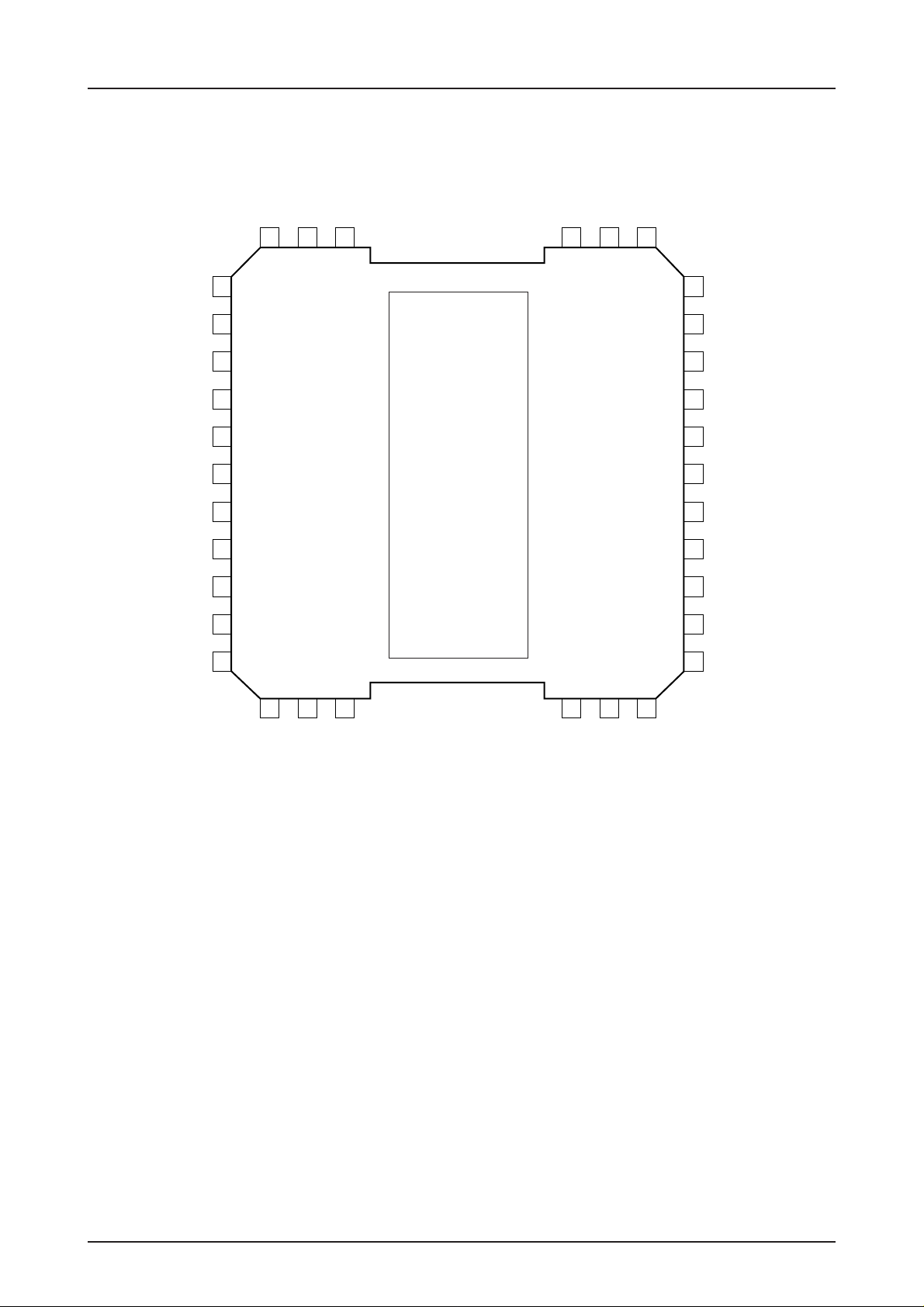
Pin Assignment
24
VG4
25
4
V
IN
26
VG3
MUTE2
VCCRF
23 22 21
LA6543
-IN
REF
RF
V
20 19 18
-OUT
REF
V
17
16
15
8
V
O
7
V
O
2
V
S
V
IN
VG2
V
IN
NC
VG1
V
IN
MUTE1
NC
27
3
28
29
2
30
31
32
1
33
34
1 2 3
2
RF
SS
V
2-OUT
SS
V
Heat sink
LA6543
4 5 6
1
RF
SS
V
1-OUT
SS
V
14
13
12
11
10
9
8
7
NC
6
V
O
5
V
O
4
V
O
3
V
O
1
V
S
2
V
O
1
V
O
Top view
A11146
No. 5973-3/7
 Loading...