

33197HA(OT) No. 5630-1/4
Overview
The LA6539M is a three-channel bridge driver (BTL)
developed for use in CD-ROM drives.
Functions
¥ Three-channel balanced transformerless (BTL) power
amplifier
¥IOmax: 1 A
¥ Muting circuit
¥ Thermal shutdown function
¥ Slew rate (SR): 0.5 V/µs (typical)
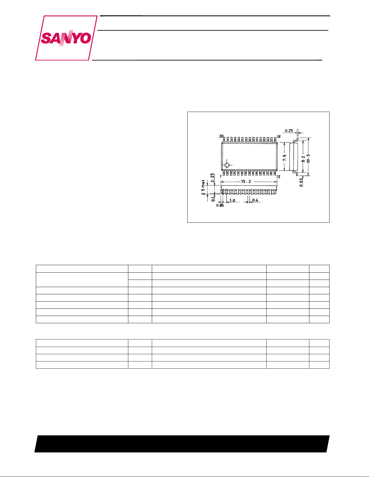
Package Dimensions
unit: mm
3073A-MFP30SLF
SANYO: MFP30SLF
[LA6539M]
LA6539M
SANYO Electric Co.,Ltd. Semiconductor Bussiness Headquarters
TOKYO OFFICE Tokyo Bldg., 1-10, 1 Chome, Ueno, Taito-ku, TOKYO, 110 JAPAN
Three-Channel CD-ROM Bridge Driver (BTL)
Monolithic Linear IC
Parameter Symbol Conditions Ratings Unit
Maximum supply voltage
V
CC
max 14 V
V
S
max Maximum rating for VS1 and VS214V
Maximum input voltage V
IN
VIN1 to VIN313V
Mute pin voltage V
MUTE
MUTE1, 2 13 V
Allowable power dissipation Pd max 0.9 W
Operating temperature Topr Ð20 to +75 ¡C
Storage temperature Tstg Ð55 to +150 ¡C
Specifications
Maximum Ratings at Ta = 25¡C
Parameter Symbol Conditions Ratings Unit
Recommended supply voltage V
CC
4 to 13 V
Operating voltage 2-1 V
S
1 The channel U operating voltage 4 to 13 V
Operating voltage 2-2 V
S
2 The channel U and W operating voltage 4 to 13 V
Operating Conditions at Ta = 25¡C
No. 5630
No. 5630-2/4
LA6539M
Parameter Symbol Conditions
Ratings
Unit
min typ max
V
CC
no-load current drain
ICC1 All outputs on (mute 1 and 2: high) *1, 2 4 8 15 mA
I
CC
2 All outputs off (mute 1 and 2: low) *1 4 10 mA
V
S
1 no-load current drain
IS1-1 Channel U: on (mute 1: high) 5 10 mA
I
S
1-2 Channel U: off (mute 1: low) 1 mA
V
S
2 no-load current drain
IS2-1 Channels V and W: on (mute 2: high) *2 10 20 mA
I
S
2-2 Channels V and W: off (mute 2: low) 1 mA
Output offset voltage V
OF
1 to VOF3 Voltage differential between the channel U and W outputs Ð50 +50 mV
Input voltage range V
IN
Voltage range for VIN1 to VIN3 0.5 5 V
Buffer amplifier output voltage
V
BUFFER
1 Voltage difference relative to 1/2 VS1 Ð50 0 +50 mV
V
BUFFER
2 Voltage difference relative to 1/2 VS2 Ð50 0 +50 mV
Output source voltage V
O
1 Output high, IO= 700 mA, all + outputs 4.4 4.7 V
Output sink voltage V
O
2 Output low, IO= 700 mA, all + outputs 0.3 0.6 V
Closed circuit voltage gain VG Bridge amplifier 6 dB
Slew rate SR 0.5 V/µs
Mute on voltage V
MUTE1, 2
The voltage applied to MUTE1 or MUTE2 at the point
1.5 2 V
where the output goes on.
Mute on current I
MUTE1, 2
The influx current to MUTE1 or MUTE2 at the point
6 10 µA
where the output goes on.
Notes: 1. When MUTE1 is high, the channel U output will be on.
2. When MUTE2 is high, the channel V and W outputs will be on.
Note: MUTE1 only operates for channel U, and MUTE2 only operates for channels V and W. MUTE1 and MUTE2 operate independently.
Continued on next page.
Truth Table
Operating Characteristics at Ta = 25¡C, VCC= 12 V, VS1 = VS2 = 5 V
Input MUTE
CH-U CH-V CH-W
(V
IN
pins) (MUTE1, 2)
U
OUT
+
U
OUT
Ð
V
OUT
+
V
OUT
Ð
W
OUT
+
W
OUT
Ð
H
H H L H L H L
L Ñ Ñ Ñ Ñ Ñ Ñ
L
H L H L H L H
L Ñ Ñ Ñ Ñ Ñ Ñ
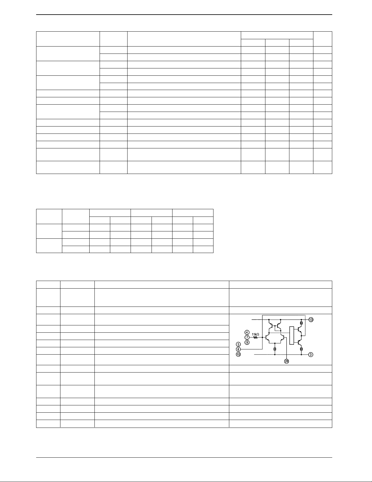
Pin Functions
Pin No. Pin Function Equivalent circuit
1, 2, 14,
15, 16, 17, RF Substrate (lowest potential)
29, 30
3 GND Ground
4 V
IN
1 Channel U input
5 V
IN
1A Channel U input (for gain adjustment)
7 V
IN
2 Channel V input
8 V
IN
2A Channel V input (for gain adjustment)
9 V
IN
3 Channel W input
10 V
IN
3A Channel W input (for gain adjustment)
6 MUTE1 Channel U output on/off control
11 BUFFER OUT1
Buffer amplifier 1 output (1/2 V
S
1: typical),
Generates the output stage reference voltage for channel U.
12 BUFFER OUT2
Buffer amplifier 2 output (1/2 V
S
2: typical),
Generates the output stage reference voltage for channels V and W.
13 V
CC
Power supply
18 NC Unused
19 MUTE2 Channels V and W on/off control
20 V
S
2 Channels V and W output stage power supply
Drive
 Loading...