SANYO LA6516 Datasheet

Overview
The LA6516 is a two-output power amplifier developed
for use in both consumer and industrial equipment.
Functions
• High slew rate (1.0 V/µs)
• High output current (IOmax = 1.0 A)
• Current limiter function
• Wide operating voltage range (±2 to 18 V)
• Supports single-voltage power supply operation (4 to 36 V)
• Thermal shutdown function
• Muting circuit (Functions for both channels; when the
mute input is high the output will be on.)
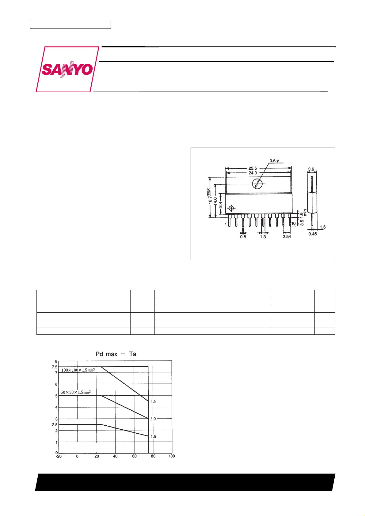
Package Dimensions
unit: mm
3046B-SIP10F
Monolithic Linear IC
Ordering number : EN5674
93097HA(OT) No. 5674-1/4
SANYO: SIP10F
[LA6516]
SANYO Electric Co.,Ltd. Semiconductor Bussiness Headquarters
TOKYO OFFICE Tokyo Bldg., 1-10, 1 Chome, Ueno, Taito-ku, TOKYO, 110 JAPAN
Two-Output Power Amplifier
LA6516
Parameter Symbol Conditions Ratings Unit
Maximum supply voltage V
CC/VEE
±18 V
Input voltage V
IN
±17 V
Allowable power dissipation Pd max 2.5 W
Operating temperature Topr –20 to +75 °C
Storage temperature Tstg –40 to +150 °C
Specifications
Absolute Maximum Ratings at Ta = 25°C
Ambient temperature, Ta — °C
Allowable power dissipation, Pd max — W
With no heat sink
With an arbitrarily large heat sink
θ
j-c = 10°C/W
Tightening torque: 39 N·cm

No. 5674-2/4
LA6516
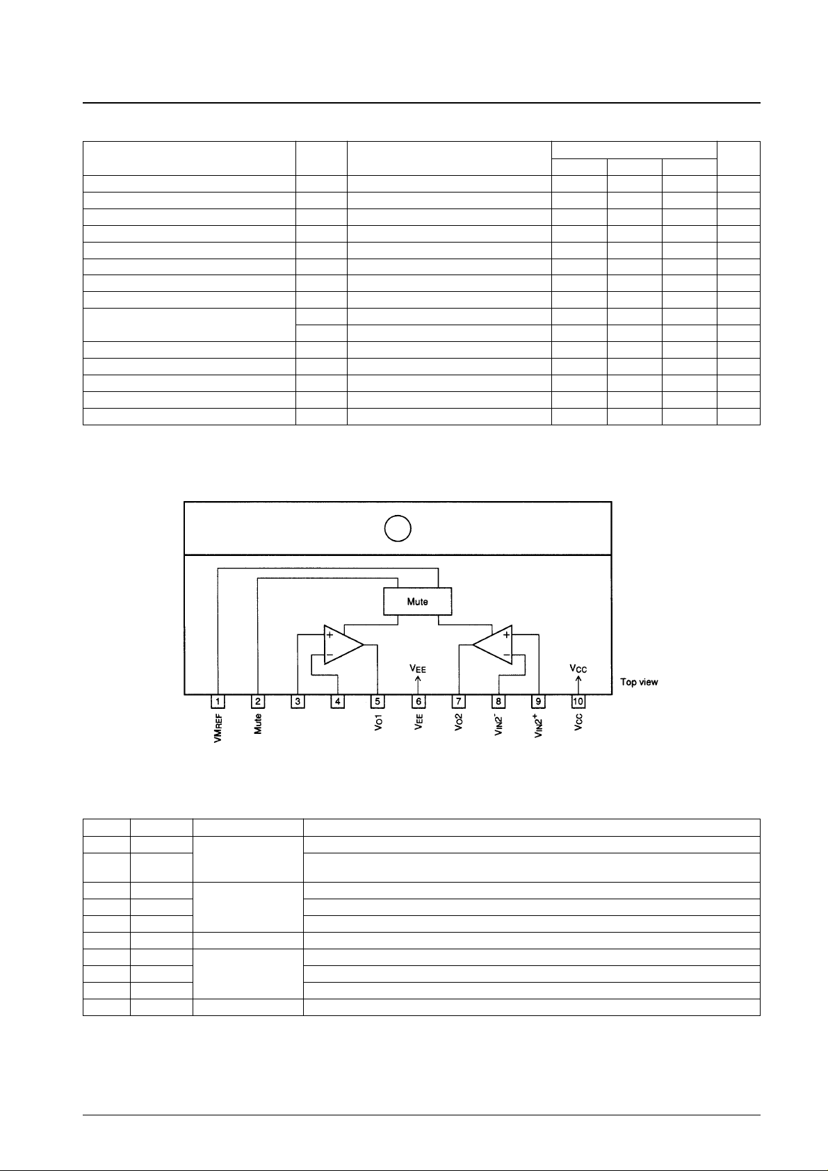
Pin Assignment
Pin Functions
Pin No. Pin Item Function
1 VM
REF
MUTE
Muting on/off reference voltage input
2 MUTE
Muting on/off signal input. Muting is activated when the MUTE pin voltage is less than the VM
REF
pin
voltage plus 1.2 V (typ).
3 VIN1
+
Amplifier 1 noninverting input
4 V
IN
1
–
AMP1 Amplifier 1 inverting input
5 V
O
1 Amplifier 1 output
6 V
EE
Negative power supply Negative power supply (–2.0 to –18.0 V)
7 V
O
2 Amplifier 2 output
8 V
IN
2
–
AMP2 Amplifier 2 inverting input
9 V
IN
2
+
Amplifier 2 noninverting input
10 V
CC
Positive power supply Positive power supply (+2.0 to +18.0 V)
Parameter Symbol Conditions
Ratings
Unit
min typ max
Quiescent current I
CC
Mute off 10 30 mA
Input offset voltage V
IO
VCC/VEE= ±15 V 2 7 mV
Input offset current I
IO
10 100 nA
Input bias current I
B
50 300 nA
Common-mode input voltage range V
ICM
–9 +8 V
Common-mode rejection ratio CMRR V
IN
= 15 Vp-p 75 dB
Supply voltage rejection ratio SVRR V
CC/VEE
= ±5 V, 15 V 30 µV/V
Voltage gain VG
O
80 dB
Maximum output voltage
V
O
1 RL= 33 Ω ±8 V
V
O
2 RL= 8 Ω ±5.6 ±6 V
Slew rate SR R
L
= 2 kΩ 1 V/µS
Limit current I
LIMIT
1 A
Muting on voltage V
MUTE ONVMREF
= 0.0 V 0.5 1.0 V
Muting off voltage VM
UTE OFFVMREF
= 0.0 V 1.0 2.0 V
Offset voltage temperature coefficient ∆ V
IO
/∆T Ta = –20 to +75°C 25 µV/°C
Electrical Characteristics at Ta = 25°C, VCC= 10 V, VEE= –10 V
V
IN
1
+
V
IN
1
–
 Loading...