

SANYO LA6503 Datasheet
Overview
The LA6503 was developed for CAV control CD-ROM
drives, and provides spindle motor driver, sled motor
driver, and sled motion/position detection circuits.
Functions and Features
• CAV control spindle motor driver
— Three-phase brushless motor driver
—IOmax = 1 A
— Built-in FG output circuit (single Hall detection
output)
— Reverse braking circuit
— Built-in start/stop circuit
— Upper side current detection for minimal loss in the
current detection resistor. Also, the voltage drop in
this resistor reduces the IC internal power
dissipation.
— Built-in thermal shutdown circuit
• Sled motor driver
— One built-in BTL driver channel
—IOmax = 1 A
— Wide dynamic range
— Built-in level shifting circuit
— Muting (output on/off) circuit
— Built-in thermal shutdown circuit
• Sled motion/position detection circuit
— Circuit that provides a pulse output corresponding to
sled motion and position
— This circuit emits 96 pulses for each rotation from
a 24-pole magnet and 90° phase difference Hall
element motors, and thus detects the distance
moved. It also provides two 48-pulse outputs with
differing phases such that the motion direction can
be detected from the phase difference between those
signals.
• Hall bias power supply
— Generates the Hall element 3-V bias voltage.
—IOmax = 30 mA, typical
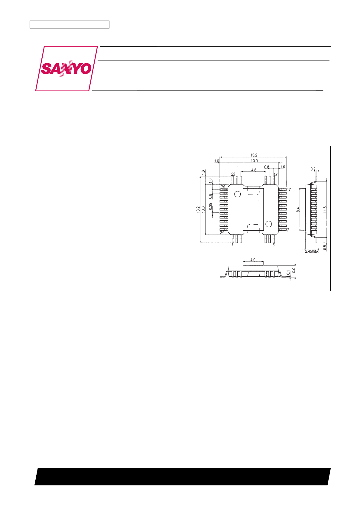
Package Dimensions
unit: mm
3219-QFP34H-C
Monolithic Linear IC
31398HA (OT) No. 5791-1/8
SANYO: QFP34H-C
[LA6503]
SANYO Electric Co.,Ltd. Semiconductor Bussiness Headquarters
TOKYO OFFICE Tokyo Bldg., 1-10, 1 Chome, Ueno, Taito-ku, TOKYO, 110-8534 JAPAN
CD-ROM Drive Spindle Motor Driver + Sled Motor
Driver + Sled Motion/Position Detector IC
LA6503
Ordering number : EN5791
No. 5791-2/8
LA6503
Parameter Symbol Conditions Ratings Unit
Supply voltage V
CC
max 7 V
Supply voltage V
M
max 14 V
Input voltage V
C
max V
CC
V
Output current I
O
max Spindle output, sled output 1 A
Allowable power dissipation Pd max Independent IC 0.77 W
Operating temperature Topr –20 to +75 °C
Storage temperature Tstg –55 to +150 °C
Specifications
Maximum Ratings at Ta = 25°C
Parameter Symbol Conditions
Ratings
Unit
min typ max
[Power Supply Current]
Current drain 1 (V
CC
) ICC1 START/STOP = MUTE = 5 V 10 20 mA
Current drain 2 (V
M
) IM1 START/STOP = MUTE = 5 V 25 50 mA
Quiescent current 1 (V
CC
) ICC2 START/STOP = MUTE = 0 V 5 10 mA
Quiescent current 2 (V
M
) IM2 START/STOP = MUTE = 0 V 1 5 mA
[Spindle Motor Block]
[Output]
Upper side saturation voltage 1 V
sourceIO
= –0.5 A 1.0 1.5 V
Lower side saturation voltage 1 V
sinkIO
= +0.5 A 0.33 0.80 V
Current limiter voltage setting V
CL
RRE= 0.43 Ω 0.32 V
[Hall Amplifier]
Common-mode input voltage range V
HCOM
1.2 VCC– 1.0 V
Input bias current V
HIB
1 µA
Minimum Hall input level V
HIN
60 mVp-p
[S/S Pin]
High-level voltage VS/SH 2.0 V
CC
V
Low-level voltage VS/SL 0.7 V
Input current IS/SI VS/S = 5 V 200 µA
Leakage current IS/SL VS/S = 0 V –30 µA
[Control]
VC pin input current I
VC
VC= V
CREF
= 2.5 V 1 5 µA
VCREF pin input current I
VCREFVC
= V
CREF
= 2.5 V 1 5 µA
Voltage gain G
VCO
∆VRF/∆V
C
0.25 Times
Rising edge threshold voltage V
CTH
V
CREF
= 2.5 V 2.35 2.65 V
Rising edge threshold voltage difference ∆V
CTHVCREF
= 2.5 V 50 150 mV
[Hall Comparator]
Input offset voltage V
HCIOFFSET
10 mV
Input hysteresis V
HCIHYS
8 mV
Output on voltage V
OU
0.3 V
Output off voltage V
OD
* 4.7 V
Output current (sink) I
sink
3 mA
Operating Characteristics at Ta = 25°C, VCC= 5 V, VM= 12 V (unless otherwise specified)
Parameter Symbol Conditions Ratings Unit
Operating supply voltage range
V
CC
4.6 to 6.0 V
V
M
4.6 to 13.0 V
Operating Conditions at Ta = 25°C
Continued on next page.
No. 5791-3/8
LA6503
Continued from preceding page.
Parameter Symbol Conditions
Ratings
Unit
min typ max
[Sled Motor Block]
Output offset voltage V
OFF
Voltage difference between outputs –50 +50 mV
Buffer input voltage range V
BIN
1.5 VCC– 1.5 V
Input voltage range V
IN
1.0 VCC– 1.5 V
Source output voltage V
O
1 RL= 8 Ω 9.5 10.1 V
Sink output voltage V
O
2 RL= 8 Ω 1.8 2.4 V
Closed-circuit voltage gain VG Bridge Amp 12 dB
Slew rate S
R
0.15 V/µs
Muting on voltage V
MUTE
The amplifier output is on when at the high level. 0.7 1.2 2.0 V
[Hall Bias (3-V Output Power Supply)]
Output voltage V
HB-OUTIOUT
= 30 mA 2.5 3.0 3.5 V
Line regulation V
HB-LINVCC
= 4.6 to 6 V, I
OUT
= 30 mA –50 +50 mV
Load regulation V
HB-LOADIOUT
= 5 to 30 mA, VCC= 5 V –200 +200 mV
Truth Table
(Spindle Motor Block)
Inputs: The “H” state is when the + input of the corresponding
phase is 0.2 V or more higher than the – input.
The “L” state is when the + input of the corresponding
phase is 0.2 V or more lower than the – input.
Note: For items marked with an asterisk (*), the Hall comparator goes to the high level when the S/S pin is off (standby mode).
Source
→ Sink
Input Control
U V W VC
1
W → V
H H L
H
V → W L
2
W → U
H L L
H
U → W L
3
V → W
L L H
H
W → V L
4
U → V
L H L
H
V → U L
5
V → U
H L H
H
U → V L
6
U → W
L H H
H
W → U L
(Sled Motor Block)
Note: “—” indicates that the amplifier output is off.
Input (V
IN
) Mute
Output
SLD-OUT+ SLD-OUT–
H
H H L
L — —
L
H L H
L — —
 Loading...