

Sanyo LA6393M Specifications
Any and all SANYO products described or contained herein do not have specifications that can handle
applications that require extremely high levels of reliability, such as life-support systems, aircraft’s
control systems, or other applications whose failure can be reasonably expected to result in serious
physical and/or material damage. Consult with your SANYO representative nearest you before using
any SANYO products described or contained herein in such applications.
SANYO assumes no responsibility for equipment failures that result from using products at values that
exceed, even momentarily, rated values (such as maximum ratings, operating condition ranges,or other
parameters) listed in products specifications of any and all SANYO products described or contained
herein.
Monolithic Linear IC
High-Performance Dual Comparator
Ordering number:ENN1103B
LA6393M
SANYO Electric Co.,Ltd. Semiconductor Company
TOKYO OFFICE Tokyo Bldg., 1-10, 1 Chome, Ueno, Taito-ku, TOKYO, 110-8534 JAPAN
Overview
The LA6393M is a high-performance dual comparator that
is capable of operating from a single power supply over a
wide range of 2V to 36V. Because of its excellent input
characteristics and low power, it can be very conveniently
applied to multisignal parallel comparator circuits that require high-density assembly.
Features
• Wide supply voltage range (Single supply : 2.0 to 36.0V,
dual supplies : ±1.0 to 18.0V).
• Wide common-mode input v oltage range (0 to VCC–1.5V).
• Open collector output enabling wired OR.
• Small current drain (0.6mA) and low power.
• Mini flat package enabling compactness of sets.
Specifications
Absolute Maximum Ratings at Ta = 25˚C
retemaraPlobmySsnoitidnoCsgnitaRtinU
egatlovylppusmumixaMV
egatlovtupnilaitnereffiDV
egnaregatlovtupniedom-nommoCV
noitapissidrewopelbawollAxamdP 003Wm
erutarepmetgnitarepOrpoT 58+ot03–
erutarepmetegarotSgtsT 521+ot55–
xam 63V
CC
DI
MCI
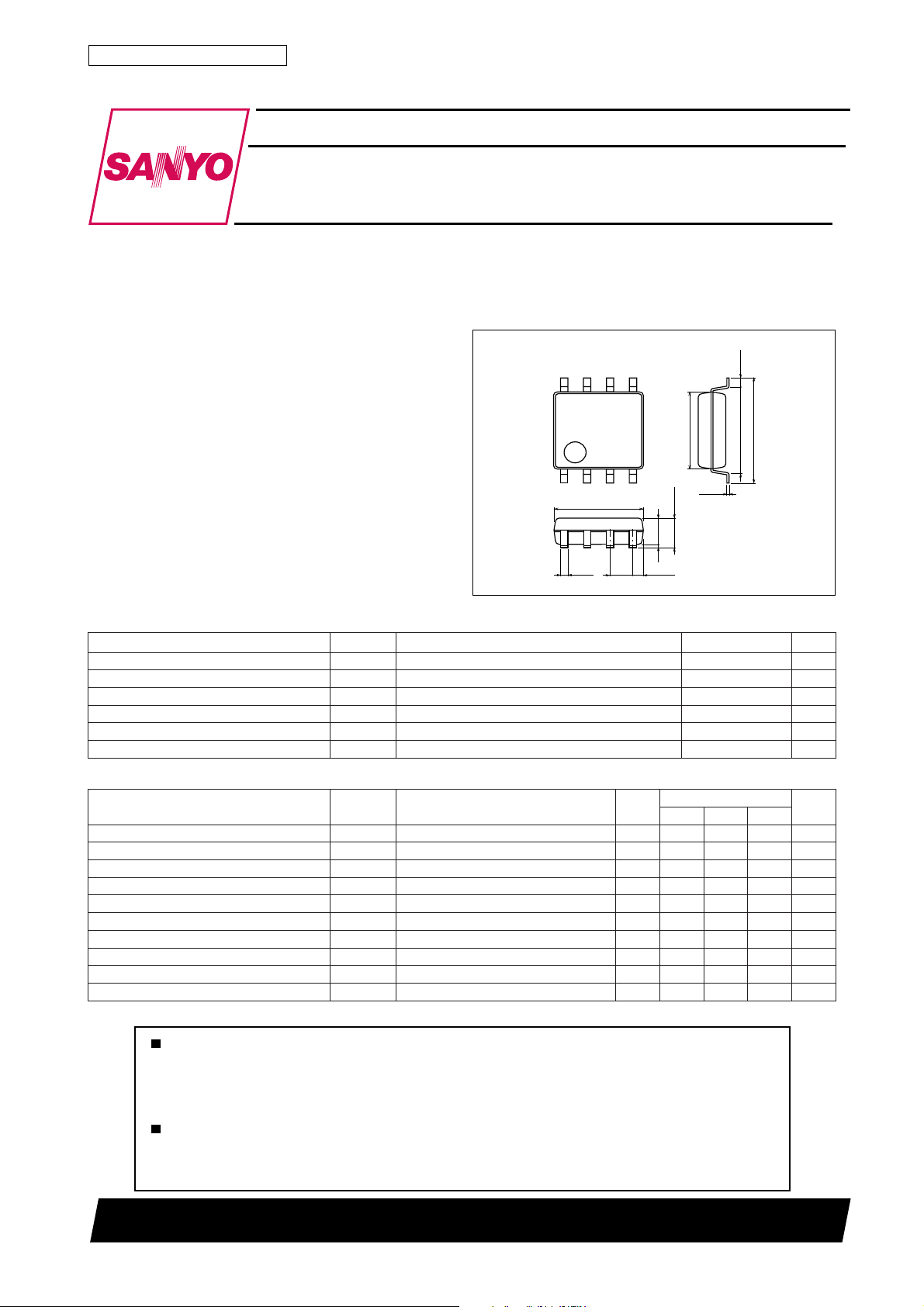
Package Dimensions
unit:mm
3032B-MFP8
[LA6393M]
8
1
5
4
5.1
1.50.1
1.270.35
0.645
4.4
1.8max
0.625
5.15
0.15
SANYO : MFP8
6.4
63V
63+ot3.0–V
˚C
˚C
Operating Characteristics at Ta = 25˚C, VCC=5V
retemaraPlobmySsnoitidnoC
egatlovtesffotupnIVOI11±5±Vm
tnerructesffotupnIIOI25±05±An
tnerrucsaibtupnIIB352052An
egnaregatlovtupniedom-nommoCV
niardtnerruCI
niagegatloVGVRLk51= Ω 5002Vm/V
emitesnopseRV
tnerrucknistuptuOI
egatlovnoitarutastuptuOV
tnerrucegakaeltuptuOI
MCI
RL=∞ 46.01Am
CC
R,V5=
LR
–
V
KNIS
NI
–
V
LO
NI
–
V
KAEL
NI
k1.5= Ω 63.1sµ
L
+
V,V1=
V,V1=
V,V0=
V,V0=
NI
+
NI
+
NI
≤ V5.17661Am
O
I,V0=
≤ Am38 2.04.0V
KNIS
V,V1=
V5=91.0An
O
40500TN (KT)/7097KI/4235MW/7282 No.1103–1/4
tseT
tiucriC
sgnitaR
nimpytxam
0
VCC5.1–
tinU
V
LA6393M
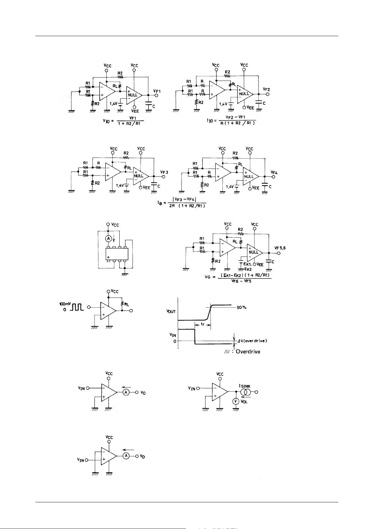
Test Circuits
1. Input offset voltage 2. Input offset current
3. Input bias current
4. Current drain 5. Voltage gain
6. Response time
7. Output sink current 8. Output saturation voltage
9. Output leakage current
No.1103–2/4
 Loading...