

SANYO LA6324NM, LA6324N Datasheet
Ordering number: EN2704B
Monolithic Linear IC
LA6324N, 6324NM
High-Performance
Quad Operational Amplifier
Overview
The LA6324 consists of four independent, high-performance,
internally phase compensated operational amplifiers that are
designed to operate from a single power supply over a wide
range of voltages. These four operational amplifiers are
packaged in a single package. As in case of conventional
general-purpose operational amplifiers, operation from dual
power supplies is also possible and the power dissipation is
low. It can be applied to various uses in commercial and
industrial equipment including all types of transducer
amplifiers and DC amplifiers.
Features
.
No phase compensation required
.
Wide operating voltage range:
3.0 V to 30.0 V (single supply)
±1.5Vto±15.0 V (dual supplies)
.
Highly resistant to dielectric breakdown
.
Input voltage range includes the neighborhood of GND level
and output voltage range V
.
Small current dissipation:
I
= 0.6 mA typ/VCC=+5V,RL=∞
CC
is from 0 to VCC− 1.5 V.
OUT
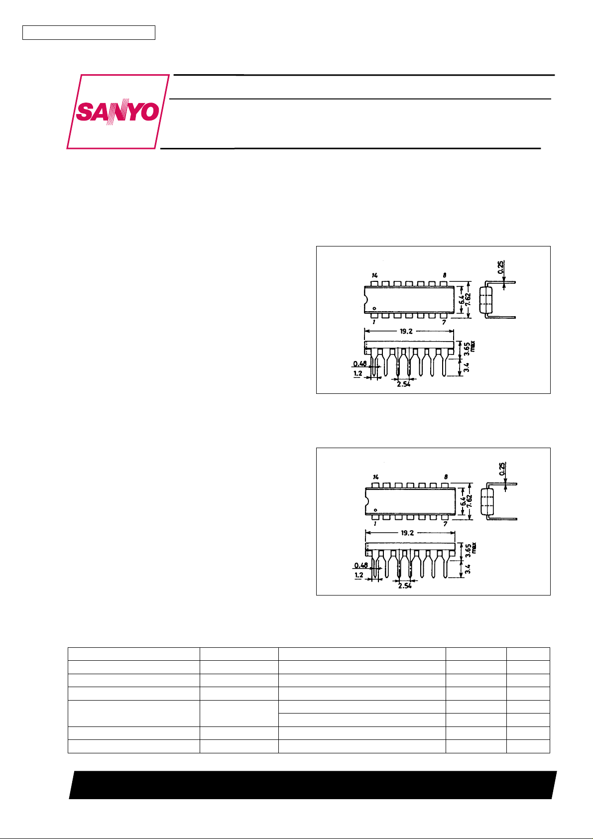
Package Dimensions
unit : mm
3003A-DIP14
[LA6324N]
SANYO : DIP14
unit : mm
3034A-MFP14
[LA6324NM]
SANYO : MFP14
Specifications
Maximum Ratings at Ta = 25°C
Parameter Symbol Conditions Ratings Unit
Maximum supply voltage V
Differential input voltage V
Maximum input voltage V
Allowable power dissipation Pd max LA6324N 720 mW
Operating temperature Topr –30 to +85 °C
Storage temperature Tstg –55 to +125 °C
max 32 V
CC
ID
max –0.3 to +32 V
IN
LA6324NM 330 mW
32 V
SANYO Electric Co.,Ltd. Semiconductor Bussiness Headquarters
TOKYO OFFICE Tokyo Bldg., 1-10, 1 Chome, Ueno, Taito-ku, TOKYO, 110 JAPAN
63096HA(II)/4138TA(KOTO) No.2704-1/5
LA6324N, 6324NM
Operating Characteristics at Ta = 25°C, VCC=+5V
Parameter Symbol Conditions Test circuit min typ max Unit
Input offset voltage V
Input offset current I
Input bias current I
Common-mode input voltage
range
IO
IIN(+)/IIN(–) 2 ±5 ±50 nA
IO
IIN(+)/IIN(–) 3 45 250 nA
B
V
ICM
Common-mode rejection ratio CMR 4 65 80 dB
Voltage gain VG V
Output voltage range V
OUT
=15V,RL^2kΩ 5 25 100 V/mV
CC
Supply voltage rejection ratio SVR 6 65 100 dB
Channel separation CS f=1kto20kHz 7 120 dB
I
Current drain
Output current (Source) I
Output current (Sink) I
CC
I
CC
source V
O
sink V
O
VCC=30V 8 1.5 3 mA
+
IN
+
IN
=1V,V
=0V,V
–
=0V 9 20 40 mA
IN
–
= 1 V 10 10 20 mA
IN
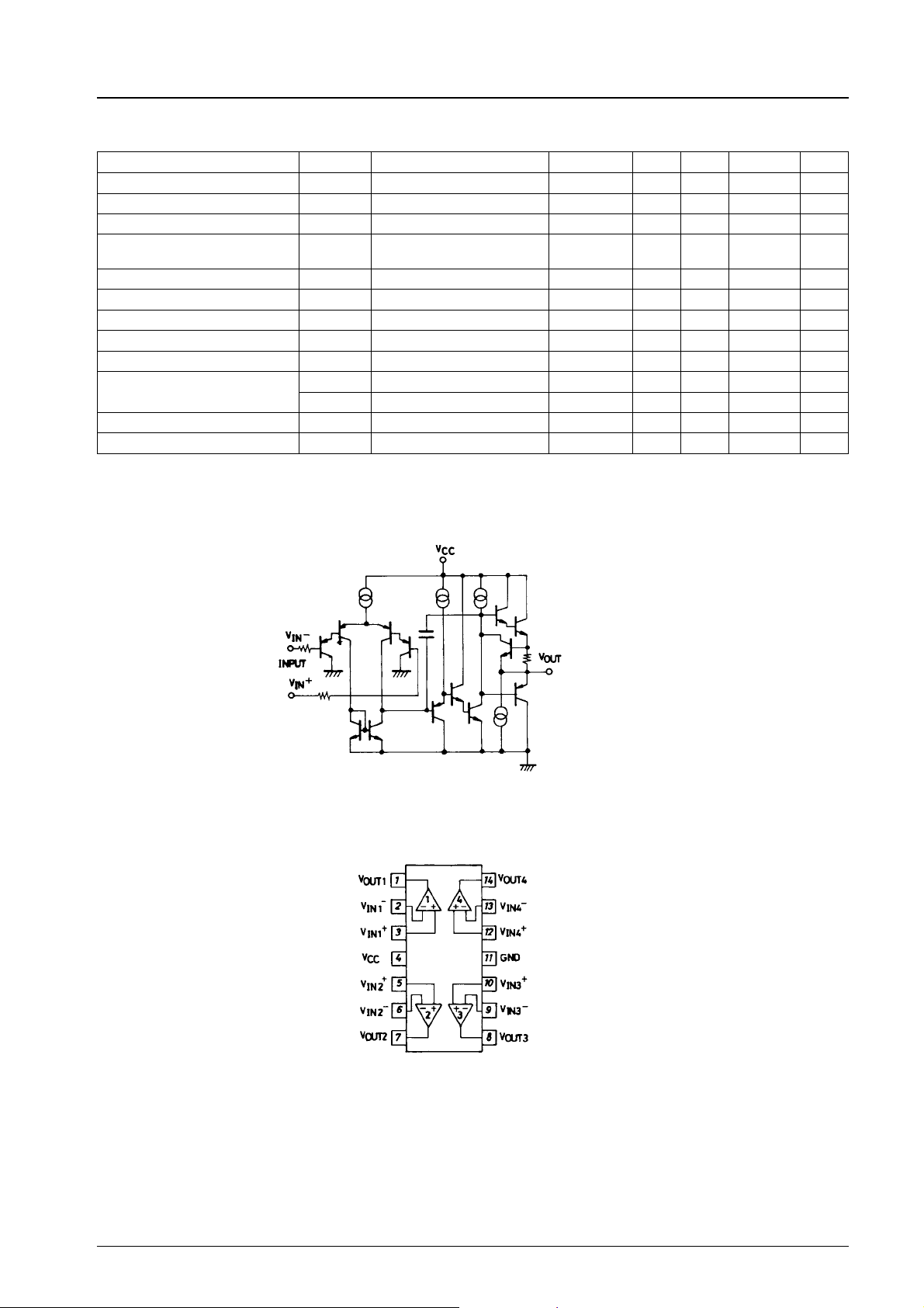
Equivalent Circuit
(1 unit)
1 ±2 ±7mV
40 V
0V
– 1.5 V
CC
– 1.5 V
CC
8 0.6 2 mA
Pin Assignment
(LA6324N, 6324NM)
Top view
No.2704-2/5
 Loading...