

Sanyo LA5691S Specifications
Any and all SANYO products described or contained herein do not have specifications that can handle
applications that require extremely high levels of reliability, such as life-support systems, aircraft’s
control systems, or other applications whose failure can be reasonably expected to result in serious
physical and/or material damage. Consult with your SANYO representative nearest you before using
any SANYO products described or contained herein in such applications.
SANYO assumes no responsibility for equipment failures that result from using products at values that
exceed, even momentarily, rated values (such as maximum ratings, operating condition ranges,or other
parameters) listed in products specifications of any and all SANYO products described or contained
herein.
Monolithic Linear IC
Voltage Regulator Driver with Watchdog Timer
(with Output ON/OFF Function)
Ordering number:ENN3244
LA5691D, 5691S
SANYO Electric Co.,Ltd. Semiconductor Company
TOKYO OFFICE Tokyo Bldg., 1-10, 1 Chome, Ueno, Taito-ku, TOKYO, 110-8534 JAPAN
Overview
The LA5691 is a single-chip voltage regulator for microcomputer system monitor use that performs the functions
of 5V output voltage control, watchdog timer, and voltage
detector. Since the LA5691 is capable of exercising output
ON/OFF controls it is especially suited for use in batterypowered equipment.
Applications
• Microcomputer system for car equipment, refrigeration/
heating equipment, office automation equipment.
Functions
• Output voltage 5V control.
• W atchdog timer .
• Reset generation at power-ON-mode.
• The enable pin can be used to exercise output ON/OFF
control (Active-low).
Features
• An external PNP transistor can be used to provide a lowsaturation voltage regulator.
• Capable of reducing of power dissipation at standby mode
(I
=300mA typ).
Q OFF
• CK input with edge detector.
• Variable detection voltage.
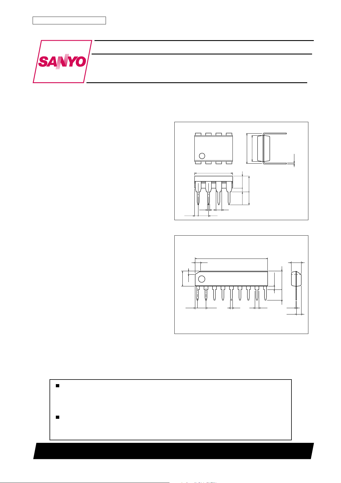
Package Dimensions
unit:mm
3001B-DIP8
8
1
0.5
0.89 2.54
unit:mm
3017C-SIP9
4.8
1.0
1
0.99
9.4
1.5
2.54
[LA5691D]
5
4
1.4
[LA5691S]
22.3
0.5
3.0
0.51min
7.62
3.9max
3.2
6.4
0.25
SANYO : DIP8
3.0
0.51min
5.7max
9
1.3
3.2
0.25
1.35
40500TN (KT)/O259YT/8037TA, TS No.3244–1/7
SANYO : SIP9
LA5691D, 5691S
Specifications
Maximum Ratings at Ta = 25˚C
retemaraPlobmySsnoitidnoCsgnitaRtinU
egatlovniplortnoC
egatlovniplortnoC
tnerrucniplortnoC
egatlovnipelbanEV
egatlovtupniKCV
egatlovnipteseRV
noitapissidrewopelbawollAxamdP 005Wm
erutarepmetgnitarepOrpoT 58+ot04–
erutarepmetegarotSgtsT 051+ot55–
V
V
I
* : A PNP transistor is connected to the LA5691D, 5691S externally to provide a low-saturation voltage regulator.
Therefore, I
≈100mA will flow, as starting current, in the VCC range where the output cannnot be regulated.
CONT
Operating Conditions at Ta = 25˚C
retemaraPlobmySsnoitidnoCsgnitaRtinU
egatlovniplortnoCV
tnerrucniplortnoC
tnerructuptuoteseR
egatlovnoitcetedteseR
I
xam
s1 06V
TNOC
xam
TNOC
xam
V*CC≥ V611Am
TNOC
xam 14V
NE
xam 52V
KC
xam 14V
SER
TNOC
xam
TNOC
I
SER
VSnim
xam
k01Rpu-lluphtiw(pu-llupRlanretxE Ω)8Am
14V
04ot6V
01Am
4V
˚C
˚C
Operating Characteristics at Ta = 25˚C, VCC=14V, IO=50mA, unless otherwise specified. See specified Test Circuit.
retemaraPlobmySsnoitidnoC
egatlovtuptuOV
noitalugereniL
noitalugerdaoL
niardtnerruCI
egatlovesiontuptuOV
egatlovtuptuofotneiciffeocerutarepmeT
egatlovecnerefeRV
egatlovtupniKClevel-HV
egatlovtupniKClevel-LV
tnerructupniKClevel-HI
tnerructupniKClevel-LI
egatlovtuptuoteserlevel-HV
1egatlovtuptuoteserlevel-LV
2egatlovtuptuoteserlevel-LV
htdiwesluptupniKCt
emityaledtuptuoteseRt
emitgodhctaWt
emittesergodhctaWt
egatlovsiseretsyhteseRsyhVVSV5.4=001002003Vm
egatloctuptuolevel-LV
tnerructnecseiuQI
egatlovlortnocFFOtuptuOV
egatlovlortnocNOtuptuOV
O
∆V
∆V
∆V
CC
∆VO/∆ aT
HI
LI
HI
LI
d
V9 ≤VCC≤ V61201Vm
1NLO
V6 ≤VCC≤ V04403Vm
2NLO
Am1 ≤IO≤ Am05403Vm
DLO
IO0=1.45.6Am
ON
FER
HRO
WKC
DW
RW
HNE
LNE
zH01 ≤f≤ V,zHk001
=5mA, –40°C≤Ta≤+85°C
I
O
VKCV5=3.07.0Am
VKC0=0.1–1.0–Aµ
1LRO
I
2LRO
VKCV5=3sµ
CtFµ1=5.7015.21sm
CtFµ1=8.30.52.6sm
CtFµ1=1.052.04.0sm
VNEV5=051003Vm
FFOO
VNEV5=003006Aµ
FFOQ
Am8=61.08.0V
SER
FFOtuptuO2V
NOtuptuO 8.0V
0=002Vµ
KC
nimpytxam
sgnitaR
8.40.52.5V
2.0±
31.181.132.1V
2V
8.40.52.5V
04002Vm
tinU
mV/˚C
8.0V
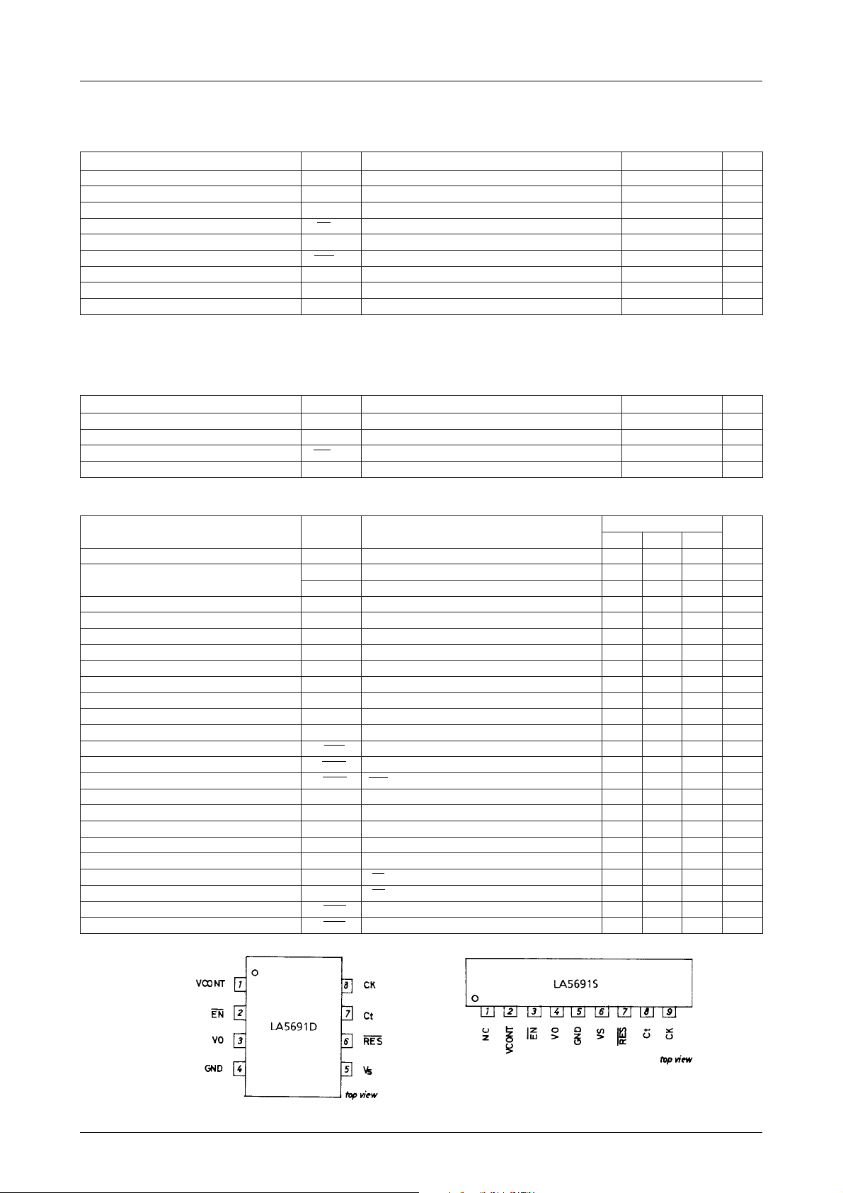
Pin Assignments
* The NC pin, which is left open, must not be used for wiring.
No.3244–2/7
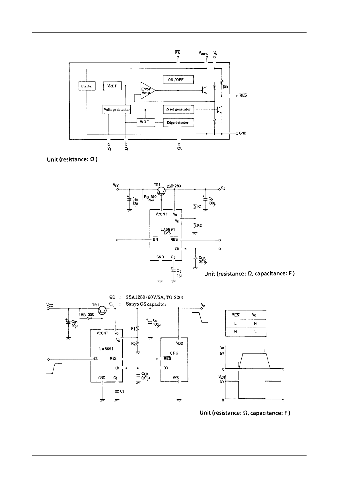
Equivalent Circuit Block Diagram
Test Circuit
LA5691D, 5691S
* The reset output contains a pull-up resistor of 10kΩ.
Sample Application Circuit
· Ct, CO: Capacitors whose value does not vary with temperature very much.
· C
: Must be used to eliminate noise in the reset output.
CK
Function Table
No.3244–3/7
 Loading...