

Page 1
Ordering number : EN3660B
O3098HA (OT)/92793TS A8-8023 No. 3660-1/7
LA5677M
SANYO Electric Co.,Ltd. Semiconductor Bussiness Headquarters
TOKYO OFFICE Tokyo Bldg., 1-10, 1 Chome, Ueno, Taito-ku, TOKYO, 110-8534 JAPAN
Dual Switching Regulator Control IC
Monolithic Linear IC
Any and all SANYO products described or contained herein do not have specifications that can handle
applications that require extremely high levels of reliability, such as life-support systems, aircraft’s
control systems, or other applications whose failure can be reasonably expected to result in serious
physical and/or material damage. Consult with your SANYO representative nearest you before using
any SANYO products described or contained herein in such applications.
SANYO assumes no responsibility for equipment failures that result from using products at values that
exceed, even momentarily, rated values (such as maximum ratings, operating condition ranges, or other
parameters) listed in products specifications of any and all SANYO products described or contained
herein.
Overview
The LA5677M supports single-input control of the outputs
of two converters of arbitrary types, including step up, step
down and inverting. Since the LA5677M supports low
voltage (3.6 to 18 V) and high frequency (1 to 500 kHz)
operation, it is ideal for use in power supplies in battery
powered portable equipment.
Features
• Operates at low voltages (3.6 to 18 V)
• Can be used with high frequency oscillators (1 to
500 kHz)
• Built-in low input malfunction prevention circuit
• Built-in timer-latch short circuit protection circuit
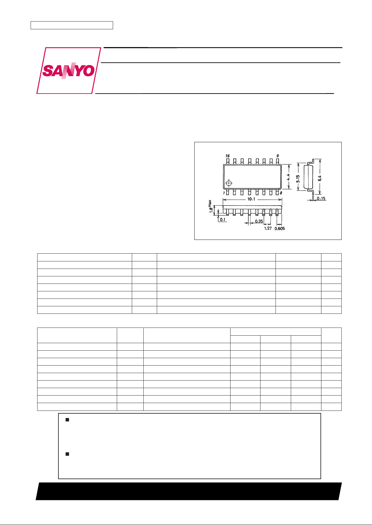
Package Dimensions
unit: mm
3035A-MFP16
Specifications
Maximum Ratings at Ta = 25°C
Parameter Symbol Conditions Ratings Unit
Maximum supply voltage V
CC
max 20 V
Error amplifier input voltage V
I
20 V
Collector output voltage V
O
20 V
Collector output current I
O
21 mA
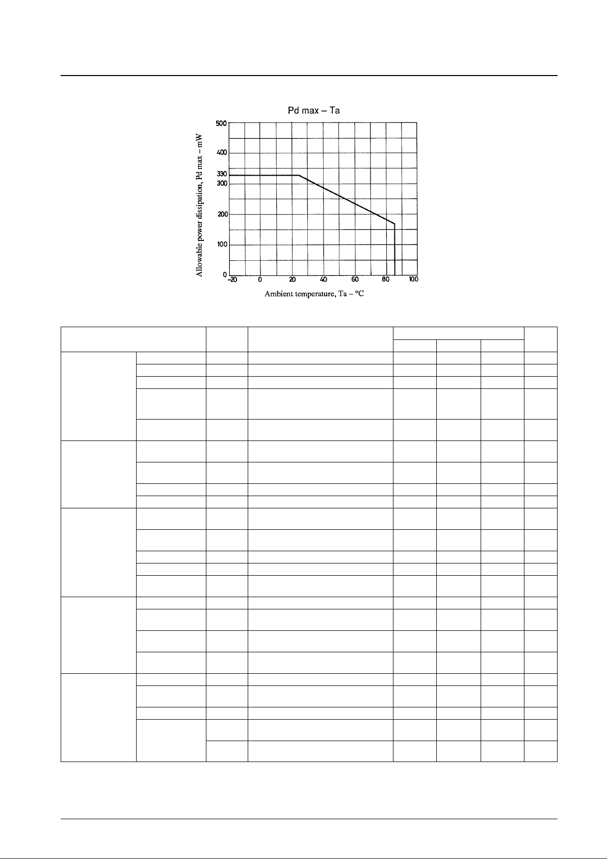
Allowable power dissipation Pd max 330 mW
Operating temperature Topr –20 to +85 °C
Storage temperature Tstg –40 to +125 °C
Parameter Symbol Conditions
Ratings
Unit
min typ max
Recommended supply voltage V
CC
3.6 18 V
Error amplifier input voltage V
I
1.05 1.45 V
Collector output voltage V
O
–0.3 +18 V
Collector output current I
O
20 mA
Feedback pin current I
FT
45 µA
Feedback resistance R
NF
100 kΩ
Timing capacitance C
T
150 15000 pF
Timing resistance R
T
5.1 100 kΩ
Oscillator frequency f
OSC
1 500 kHz
SANYO: MFP16
[LA5677M]
Operating Conditions at Ta = 25°C
Page 2
No. 3660-2/7
LA5677M
Parameter Symbol Conditions
Ratings
Unit
min typ max
Output voltage Vref I
OR
= 1 mA 2.40 2.50 2.60 V
Line regulation V
line
VCC= 3.6 to 18 V 2 10 mV
Load regulation V
loadIOR
= 0.1 to 1 mA 1 7.5 mV
Reference voltage
Output voltage
block
temperature ±0.2 %
variation
Short circuit output
I
OSC
Vref = 0 V 3 10 30 mA
current
High level threshold
V
tH
IOR= 0.1 mA 2.70 V
voltage
Low input malfunction Low level threshold
V
tL
IOR= 0.1 mA 2.58 V
prevention block voltage
Hysteresis Vhys I
OR
= 0.1 mA 80 120 mV
Reset voltage Vr I
OR
= 0.1 mA 1.5 1.9 V
Input threshold
Vtpc 1.02 1.16 1.30 V
voltage
Input standby
Vstby No pull-up 0.78 V
Protection circuit
voltage
block Input latch voltage V
1
No pull-up 0.74 V
Input source current Ibpc When VS.C.P is 1.0 V 12 18 27 µA
Comparator
Vtc Pins 5, 12 1.2 V
threshold voltage
Oscillator frequency fosc Ct = 330 pF, Rt = 10 kΩ 200 kHz
fosc standard
∆f
A
All values agree 10 %
deviation
Oscillator block Frequency variation
∆f
V
VCC= 3.6 to 18 V 1 %
1 (V
CC
)
Frequency variation
∆ft ±0.4 %
2 (Ta)
Input bias current Ibdt 1 µA
Latch mode source
Idt 230 µA
current
Idle period
Latch input voltage Vdt Iodt = 40 µA 2.3 V
adjustment circuit
Vt0 With a duty cycle of 0% 2.05 2.25 V
block
Input threshold
voltage
Vt100
fosc = 10 kHz,
1.20 1.45 V
With a duty cycle of 100%
Continued on next page.
Page 3
Continued from preceding page.
Pin Functions
No. 3660-3/7
LA5677M
Parameter Symbol Conditions
Ratings
Unit
min typ max
Input offset voltage V
IO
With V (pins 5, 12) = 1.25 V –6 +6 mV
Input offset current I
IO
With V (pins 5, 12) = 1.25 V –100 +100 nA
Input bias current I
B
With V (pins 5, 12) = 1.25 V 160 500 nA
Common mode
V
ICR
VCC= 3.6 to 18 V 1.05 1.45 V
input voltage range
Open loop gain A
V
RNF= 200 kΩ 80 dB
Unity gain
G
B
1.5 MHz
bandwidth
Error amplifier block
Common mode
CMRR 80 dB
rejection ratio
Maximum output
V
O
+ m Vref – 0.1 V
voltage amplitude (1)
Maximum output
VO– m 1.0 V
voltage amplitude (2)
Output sink current
IO+ m
VID= –0.1 V, VO= 1.25 V 1.6 mA
(pins 5, 12)
Output source
IO– m
VID= 0.1 V, VO= 1.25 V –70 µA
current (pins 5, 12)
Output leakage
I
leak
VO= 18 V 10 µA
current
Output block
Output saturation
Vsat IO= 10 mA 1.0 2 V
voltage
Short circuit output
I
OS
VO= 6 V 60 mA
current
Vt0 With a duty cycle of 0% 2.05 2.25 V
Input threshold
voltage
Vt100
fosc = 10 kHz,
1.20 1.45 V
PWM comparator
With a duty cycle of 100%
block
Input sink current
With V (pins 5, 12) = 1.25 V 1.6 mA
(pins 5, 12)
Input source current
With V (pins 5, 12) = 1.25 V –70 µA
(pins 5, 12)
Standby current I
CC
1 Output off state 1.6 2.2 mA
Whole device Average supply
I
CC
2 RT= 10 kΩ 1.9 2.6 mA
current
No. Pin Function No. Pin Function
1 C
T
Triangle wave oscillator capacitor connection 9 V
CC
Power supply input
2 R
T
Triangle wave oscillator resistor connection 10 OUT2 Output 2
3 OP1+ Error amplifier 1 + input 11 DEAD TIME2 Dead time 2 control
4 OP1– Error amplifier 1 – input 12 OP2
OUT
Error amplifier 2 output
5 OP1
OUT
Error amplifier 1 output 13 OP2– Error amplifier 2 – input
6 DEAD TIME1 Dead time 1 control 14 OP2+ Error amplifier 2 + input
7 OUT1 Output 1 15 S. C. P Short circuit protection circuit connection
8 GND Ground connection 16 Vref Reference voltage (2.5 V)
Page 4

Equivalent Circuit Block Diagram
Operation Overview
1. Reference Voltage Block
The reference voltage block uses a 2.5 V reference voltage. This voltage is made available to external circuits from
pin 16, and at the same time is used as the reference power supply by internal circuits.
2. Low Input Malfunction Prevention Circuit Block
The low input malfunction prevention circuit prevents incorrect operation when the power supply is brought up or
during brief voltage drops. After power is applied and the reference voltage reaches Vbe, the output transistors are
held off until the power supply voltage becomes 2.72 V (typical). The dead time control pin voltage is held at the
high level (Vref) and the short circuit protection pin is held low (the initial state). Since this circuit has a hysteresis of
120 mV (typical) chattering due to power supply ripple can be prevented to a certain extent.
3. Timer-Latch Short Circuit Protection Circuit
During output overload, the timer-latch short circuit protection circuit’s short circuit protection comparator turns off
Q86 when the error amplifier inputs a low level signal (a voltage less than Vref/2) to one or both of the short circuit
protection comparator’s two non-inverting inputs. At this time the pin 15 voltage increases from about 0.75 V (steady
state) towards Vref as the external capacitor is charged from Vref through resistor R41 (80 kΩ). When the capacitor is
charged to about 1.2 V, the protection latch is set, the output transistors are turned off, and the idle time becomes 100%.
This also turns on Q97 which resets the protection enable state. The latch circuit reset voltage is under 1.9 V (typical).
VPE1 = Vref {1 – exp (–t1/R41•CPT)}
VPE2 = Vref {1 – exp (–t2/R41•CPT)}
0.75 = 2.5 {1 – exp (–t1/80 k•CPT)}
1.20 = 2.5 {1 – exp (–t2/80 k•CPT)}
t1 = 28.56 k•C
PT
t2 = 52.31 k•C
PT
tPT= t2 – t1 = 23.75 k•C
PT
CPT= 42.1 × tPT[µF]
No. 3660-4/7
LA5677M
Page 5

Figure 1 Timer-Latch Short Circuit Protection Circuit
Figure 2 Timing Resistance/Oscillator Frequency Characteristics
4. Triangle Wave Oscillator Block
The triangle wave oscillator generates an essentially symmetric triangle wave using a timing capacitor and resistor
attached to the CTpin (pin 1) and the RTpin (pin 2), respectively. The voltage amplitude is between 1.4 and 2.0 V
with pin 2 stabilized at 1 V. The oscillator frequency is determined by the external capacitor and resistor.
5. Idle Period Adjustment Circuit Block
The idle period adjustment circuit consists of PWM comparators 1 and 2, each of which has one non-inverting and
two inverting inputs. The output pulse width (on time) is controlled according to the input voltage. Pins 6 and 11 are
dead time control pins, and are used to limit the maximum value of the pulse width. A pin voltage of 2.05 V
(Typical) or over results in the output being off for the whole period, and a pin voltage of 1.45 V (Typical) or lower
results in the output being on for the whole period.
No. 3660-5/7
LA5677M
Page 6

No. 3660-6/7
LA5677M
6. Error Amplifier Block
Error amplifiers 1 and 2 are amplifiers for detecting the output voltages, i.e., the LA5677M application system output
voltages. Since the common mode input voltage range is 1.05 to 1.45 V, we recommend setting their input voltages
to Vref/2. Pins 5 and 12 are the output pins, and the gain is set and the frequency characteristics adjusted with a
resistor and a capacitor connected between the outputs and the non-inverting inputs of each amplifier. The outputs
are also connected to the short circuit protection circuit detection circuit.
7. Output Block
The outputs are single end open collector outputs with an NPN Darlington pair structure.
Sample Application Circuit: +5 V, 1 A step-down converter and –5 V, 0.5 A polarity inverting converter using a
12 V input
Page 7

PS No. 3660-7/7
LA5677M
This catalog provides information as of December, 1998. Specifications and information herein are
subject to change without notice.
Specifications of any and all SANYO products described or contained herein stipulate the performance,
characteristics, and functions of the described products in the independent state, and are not guarantees
of the performance, characteristics, and functions of the described products as mounted in the customer’s
products or equipment. To verify symptoms and states that cannot be evaluated in an independent device,
the customer should always evaluate and test devices mounted in the customer’s products or equipment.
SANYO Electric Co., Ltd. strives to supply high-quality high-reliability products. However, any and all
semiconductor products fail with some probability. It is possible that these probabilistic failures could
give rise to accidents or events that could endanger human lives, that could give rise to smoke or fire,
or that could cause damage to other property. When designing equipment, adopt safety measures so
that these kinds of accidents or events cannot occur. Such measures include but are not limited to protective
circuits and error prevention circuits for safe design, redundant design, and structural design.
In the event that any or all SANYO products (including technical data, services) described or contained
herein are controlled under any of applicable local export control laws and regulations, such products must
not be exported without obtaining the export license from the authorities concerned in accordance with the
above law.
No part of this publication may be reproduced or transmitted in any form or by any means, electronic or
mechanical, including photocopying and recording, or any information storage or retrieval system,
or otherwise, without the prior written permission of SANYO Electric Co., Ltd.
Any and all information described or contained herein are subject to change without notice due to
product/technology improvement, etc. When designing equipment, refer to the “Delivery Specification”
for the SANYO product that you intend to use.
Information (including circuit diagrams and circuit parameters) herein is for example only; it is not
guaranteed for volume production. SANYO believes information herein is accurate and reliable, but
no guarantees are made or implied regarding its use or any infringements of intellectual property rights
or other rights of third parties.
 Loading...