

Page 1
Any and all SANYO products described or contained herein do not have specifications that can handle
applications that require extremely high levels of reliability, such as life-support systems, aircraft’s
control systems, or other applications whose failure can be reasonably expected to result in serious
physical and/or material damage. Consult with your SANYO representative nearest you before using
any SANYO products described or contained herein in such applications.
SANYO assumes no responsibility for equipment failures that result from using products at values that
exceed, even momentarily, rated values (such as maximum ratings, operating condition ranges,or other
parameters) listed in products specifications of any and all SANYO products described or contained
herein.
Monolithic Linear IC
Multifunctional V oltage Regulator
Ordering number:ENN3238A
LA5668
SANYO Electric Co.,Ltd. Semiconductor Company
TOKYO OFFICE Tokyo Bldg., 1-10, 1 Chome, Ueno, Taito-ku, TOKYO, 110-8534 JAPAN
Overview
The LA5668 is a multifunctional voltage regulator IC especially suited for use in portable musical instrument applications.
Functions and Features
• Power output : 1.0A
• Analog output : 5.5V, 0.1A
• Digital output : 5.0V, 0.1A
• Low I
Specifications
Maximum Ratings at Ta = 25˚C
at power-OFF mode (APO=OFF) : 35µA typ
CC
retemaraPlobmySsnoitidnoCsgnitaRtinU
egatlovtupnI
tnerructuptuO
noitapissidrewopelbawollAxamdP 54.2W
erutarepmetgnitarepOrpoT 58+ot03–
erutarepmetegarotSgtsT 521+ot04–
VNIxam 81V
V
xam 81V
NID
I
xam 0.1A
OC
I
xam 001Am
OA
I
xam 001Am
OD
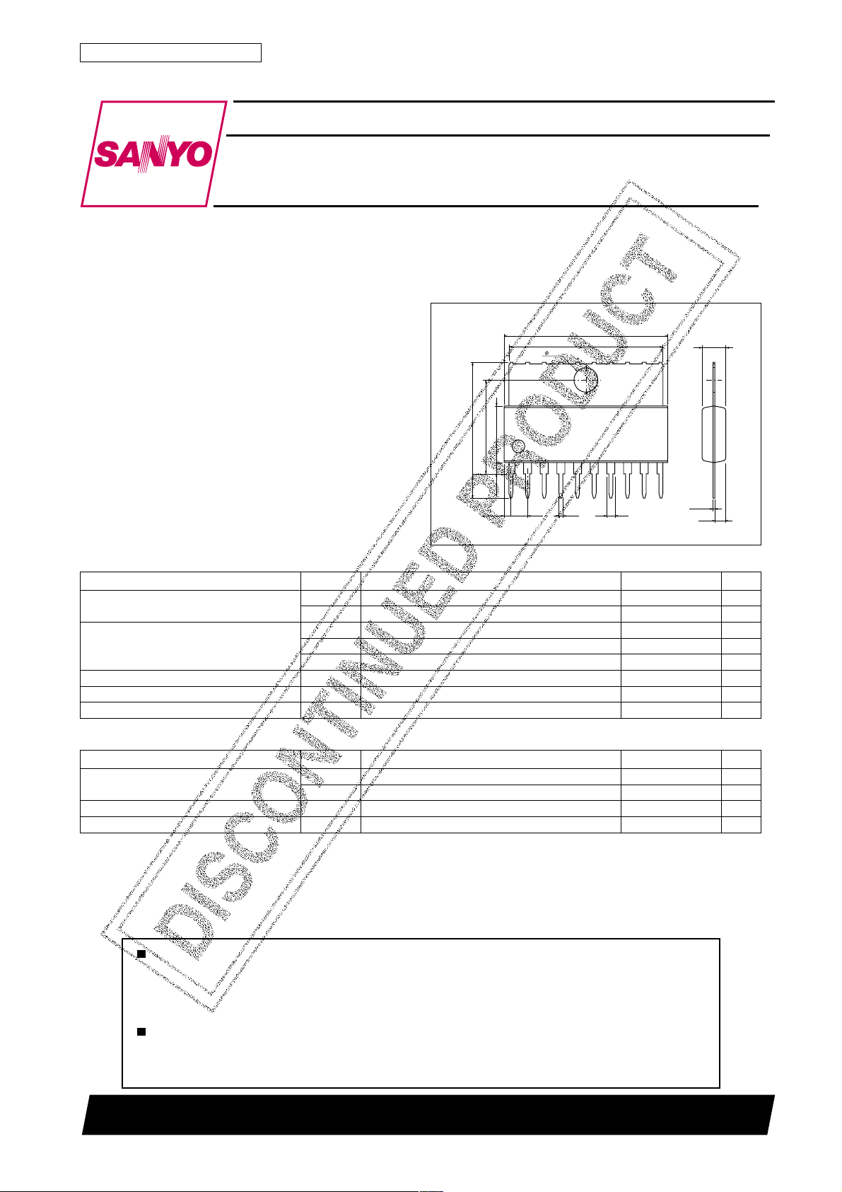
Package Dimensions
unit:mm
3046B-SIP10F
[LA5668]
25.5
24.0
3.6
14.0
16.7max
8.4
3.5
1.6 min
1.32
2.54
0.5
3.6
101
1.3
0.45
1.6
SANYO : SIP10F
˚C
˚C
Operating Conditions at Ta = 25˚C
retemaraPlobmySsnoitidnoCsgnitaRtinU
V
egatlovtupnI
egatlovetats-nonipOPAV
egatlovetats-ffonipOPAV
NI
V
NID
NOOPA
FFOOPA
42000TN (KT)/O169TA, TS No.3238–1/4
51ot0.7V
51ot0.7V
Vot2
V
NI
3.0+ot3.0–V
Page 2
LA5668
Operating Characteristics at Ta = 25˚C (V
retemaraPlobmySsnoitidnoC
I
I
V
V
V
V
OA
V
O1D
V
O2D
V
1A
V
2A
V
O1D
V
O2D
V
V
V
R
R
C
C
AV-DIOA
1CC
2CC
OA
O1D
O2D
Ad
Dd
COd
Ar
Dr
OPA
V
V
VAV-
tnerructnecseiuQ
egatlovtuptuO
noitalugereniL
noitalugerdaoL
ecnereffidegatlovtuptuo-tupnI
noitcejerelppiR
tnerructupniOPAI
C
C
D
egatlovetats-noV
egatlovetats-ffoV
egatlovV
IN=VDIN=VAPO
V
V0=5305Aµ
OPA
V
V=
OPA
I
V
V
eniL0.7 ≤VNI≤ I,V31
eniL0.7 ≤VNI≤ V,V31
eniL0.7 ≤VNI≤ V,V31
daoL1≤I
daoL1≤I
daoL1≤IOD≤ V,Am01
daoL1≤IOD≤ V,Am08
VNIVVNIVI
V
NOV
FFOVAVtaegatlov
NI
Am05=50.55.559.5V
OA
OPA
V=NII,
OPA
≤ Am0405Vm
O1A
≤ Am08001Vm
O2A
O
O
DC
V5=6668321Aµ
OPA
A
=9V, C1=C2=C3=22µF unless otherwise specified)
sgnitaR
nimpytxam
0.80.11Am
I,V0=
Am5=55.40.554.5V
OD
Am05=55.40.554.5V
OD
Am05=05Vm
OA
I,V0=
Am5=05Vm
OD
Am05=05Vm
OD
I,FFO%5
I,FFO%5
NI
Am001=04Bd
Am001=54Bd
VtaAm51=
Am05=9.02.1V
OA
Am05=9.02.1V
OD
V9=1.16.1V
CC
V9,V5.5=3.0– V
VtadV:
VtadV:
I,Am52=
OPA
V=NII,
OPA
V0=05Vm
OPA
V=
OPA
NI
O
O
V,Am005=
Vtaegatlov
OD
Vta
NIV-D
I,zH021,zH05=f
OA
I,zH021,zH05=f
OD
V0=5.1V
OPA
V0=5.0V
OPA
tinU
05Vm
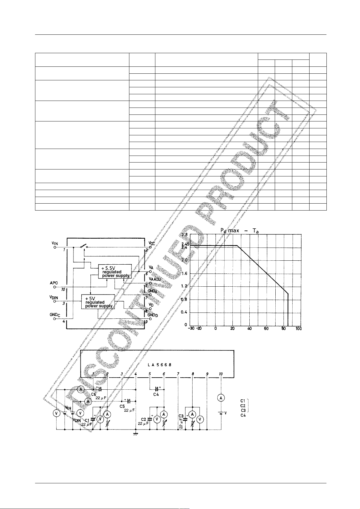
Block Diagram and Pin Assignment
Test Circuit
Allowable power dissipation, Pd max – W
Ambient temperature, Ta – °C
OSC prevention, stabilization
rise adjustment
V
A
No.3238–2/4
Page 3

Sample Application Circuit
LA5668
OSC prevention, stabilization
rise adjustment
V
A
– µA
CC1
Current drain, I
– V
AOUT
Output voltage, V
Supply voltage, VCC – V
– µA
CC2
Current drain, I
Supply voltage, VCC – V
– V
D2OUT
Output voltage, V
Supply voltage, VCC – V
Supply voltage, VCC – V
No.3238–3/4
Page 4

LA5668
– V
AOUT
Output voltage, V
– V
dcOUT
Output current, I
AOUT
– mA
– V
D2OUT
Output voltage, V
Output current, I
D2OUT
– mA
Input-output voltage difference, V
Output current, I
COUT
– A
Specifications of any and all SANYO products described or contained herein stipulate the performance,
characteristics, and functions of the described products in the independent state, and are not guarantees
of the performance, characteristics, and functions of the described products as mounted in the customer's
products or equipment. To verify symptoms and states that cannot be evaluated in an independent device,
the customer should always evaluate and test devices mounted in the customer's products or equipment.
SANYO Electric Co., Ltd. strives to supply high-quality high-reliability products. However, any and all
semiconductor products fail with some probability. It is possible that these probabilistic failures could
give rise to accidents or events that could endanger human lives, that could give rise to smoke or fire,
or that could cause damage to other property. When designing equipment, adopt safety measures so
that these kinds of accidents or events cannot occur. Such measures include but are not limited to protective
circuits and error prevention circuits for safe design, redundant design, and structural design.
In the event that any or all SANYO products(including technical data,services) described or
contained herein are controlled under any of applicable local export control laws and regulations,
such products must not be exported without obtaining the export license from the authorities
concerned in accordance with the above law.
No part of this publication may be reproduced or transmitted in any form or by any means, electronic or
mechanical, including photocopying and recording, or any information storage or retrieval system,
or otherwise, without the prior written permission of SANYO Electric Co. , Ltd.
Any and all information described or contained herein are subject to change without notice due to
product/technology improvement, etc. When designing equipment, refer to the "Delivery Specification"
for the SANYO product that you intend to use.
Information (including circuit diagrams and circuit parameters) herein is for example only ; it is not
guaranteed for volume production. SANYO believes information herein is accurate and reliable, but
no guarantees are made or implied regarding its use or any infringements of intellectual property rights
or other rights of third parties.
This catalog provides information as of April, 2000. Specifications and information herein are subject to
change without notice.
PS No.3238–4/4
 Loading...